1
White Electronic Designs Corporation (508) 366-5151 www.whiteedc.com
Oct. 2002 Rev. 9A
ECO #15655
EDI8F3265C
FEATURES
n 64Kx32 bit CMOS Static
n Random Access Memory
Access Times 12 through 25ns
Individual Byte Selects
Output Enable Function
Fully Static, No Clocks
TTL Compatible I/O
n High Density Packaging
64 Pin SIMM, No. 30-Straight
64 Pin SIMM, No. 342 Angled
64 Pin ZIP, No. 87
JEDEC Standard Pinout
Common Data Inputs and Outputs
n Single +5V (±10%) Supply Operation
64Kx32 Static RAM CMOS, High Speed Module
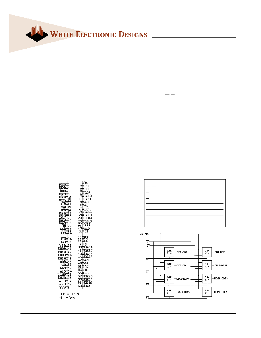
The EDI8F3265C is a high speed 2 megabit Static RAM module
organized as 64Kx32. This module is constructed from eight
64Kx4 Static RAMs in SOJ packages on an epoxy laminate (FR4)
board.
Four chip Enables (Eÿ-E3) are used to independently enable the
four bytes. Reading or writing can be executed on individual
bytes or any combination of multiple bytes through proper use of
selects.
The EDI8F3265C is offered in a both 64 lead SIMM and 64 pin
ZIP packages, which enable two megabits of memory to be
placed in less than 1.2 square inches of board space.
All inputs and outputs are TTL compatible and operate from a
single 5V supply. Fully asynchronous circuitry is used, requiring
no clocks or refreshing for operation and providing equal access
and cycle times for ease of use.
PIN CONFIGURATIONS AND BLOCK DIAGRAM
PIN NAMES
DESCRIPTION
A0-A15
Address Inputs
Eÿ-E3
Chip Enable
W
Write Enable
G
Output Enable
DQÿ-DQ3
Common Data Input/Output
VCC
Power (+5V±10%)
VSS
Ground
NC
No Connection
2
White Electronic Designs Corporation (508) 366-5151 www.whiteedc.com
Oct. 2002 Rev. 9A
ECO #15655
EDI8F3265C
ABSOLUTE MAXIMUM RATINGS*
RECOMMENDED DC OPERATING CONDITIONS
DC ELECTRICAL CHARACTERISTICS
*Typical: TA = 25∞C, VCC = 5.0V
CAPACITANCE
TRUTH TABLE
These parameters are sampled, not 100% tested.
AC TEST CONDITIONS
(note: For TEHQZ,TGHQZ and TWLQZ, CL = 5pF)
*Stress greater than those listed under "Absolute Maximum Ratings" may cause
permanent damage to the device. This is a stress rating only and functional operation
of the device at these or any other conditions greater than those indicated in the
operational sections of this specification is not implied. Exposure to absolute maximum
rating conditions for extended periods may affect reliability.
Voltage on any pin relative to VSS
-0.5V to 7.0V
Operating Temperature TA (Ambient)
Commercial
0∞C to +70∞C
Industrial
-40∞C to +85∞C
Storage Temperature
Plastic
-55∞C to +125∞C
Power Dissipation
8.0 Watt
Output Current
20 mA
Parameter
Sym
Min
Typ
Max
Units
Supply Voltage
VCC
4.5
5.0
5.5
V
Supply Voltage
VSS
0
0
0
V
Input High Voltage
VIH
2.2
--
6.0
V
Input Low Voltage
VIL
-0.3
--
0.8
V
Input Pulse Levels
VSS to 3.0V
Input Rise and Fall Times
5ns
Input and Output Timing Levels
1.5V
Output Load
1TTL, CL =30pFI
G
E
W
Mode
Output
Power
X
H
X
Standby
High Z
ICC2, ICC3
H
L
H
Output Deselect
High Z
ICC1
L
L
H
Read
DOUT
ICC1
X
L
L
Write
DIN
ICC1
(f=1.0MHz, VIN=VCC or VSS)
Parameter
Sym
Max
Unit
Input Capacitance
(Except DQ Pins)
CI
60
pF
Capacitance (DQ Pins)
CD/Q
20
pF
Input (E)
CC
20
pF
Input (W) Line (G)
CW
60
pF
Parameter
Sym
Conditions
ns
Min Typ* Max
Units
Operating Power
ICC1
W, E = VIL, II/O = 0mA,
12-15ns
-- 880 1120
mA
Supply Current
Min Cycle
20-25ns
740 980
mA
Standby (TTL) Power
ICC2
E ≥ VIH, VIN £ VIL
-- 150 280
mA
Supply Current
VIN ≥ VIH
Full Standby Power
ICC3
E ≥ VCC-0.2V
-- 80 160
mA
Supply Current
VIN ≥ VCC-0.2V or
CMOS
VIN £ 0.2V
Input Leakage Current
ILI
VIN = 0V to VCC
-- -- ±20
µA
Output Leakage Current
ILO
V I/O = 0V to VCC
-- -- ±80
µA
Output High Voltage
VOH
IOH = -4.0mA
2.4 --
--
V
Output Low Voltage
VOL
IOL = 8.0mA
-- -- 0.4
V

3
White Electronic Designs Corporation (508) 366-5151 www.whiteedc.com
Oct. 2002 Rev. 9A
ECO #15655
EDI8F3265C
AC CHARACTERISTICS READ CYCLE
READ CYCLE 1 - W HIGH, G, E LOW
Note 1: Parameter guaranteed, but not tested.
Symbol
12ns
15ns
20ns
25ns
JEDEC
Alt.
Min Max
Min
Max Min
Max Min
Max Units
Read Cycle Time
TAVAV
TRC
12
15
20
25
ns
Address Access Time
TAVQV
TAA
12
15
20
25
ns
Chip Enable
Access Time
TELQV TACS
12
15
20
25
ns
Chip Enable to
Output in Low Z (1)
TELQX TCLZ
3
3
3
3
ns
Chip Disable to
Output in High Z (1)
TEHQZ TCHZ
0
8
0
8
0
10
0
12
ns
Output Hold from
Address Change
TAVQX TOH
3
3
3
3
ns
Output Enable to
Output Valid
TGLQV TOE
8
8
10
15
ns
Output Enable to
Output in Low Z (1)
TGLQX TOLZ
0
0
0
0
ns
Output Disable to
Output in High Z(1)
TGHQZ TOHZ
0
6
0
6
0
8
0
10
ns
ADDRESS 1
ADDRESS 2
TAVAV
DATA 1
DATA 2
TAVQV
TAVQX
A
Q

4
White Electronic Designs Corporation (508) 366-5151 www.whiteedc.com
Oct. 2002 Rev. 9A
ECO #15655
EDI8F3265C
Note 1: Parameter guaranteed, but not tested.
AC CHARACTERISTICS WRITE CYCLE
READ CYCLE 2 - W HIGH
Symbol
12ns
15ns
20ns
25ns
Parameter
JEDEC
Alt.
Min Max
Min
Max Min
Max Min
Max Units
Write Cycle Time
TAVAV TWC
12
15
20
25
ns
Chip Enable to
TELWH TCW
10
10
15
20
ns
End of Write
TELEH TCW
10
10
15
20
ns
Address Setup Time
TAVWL
TAS
0
0
2
2
ns
TAVEL
TAS
0
0
2
2
ns
Address Valid to
TAVWH TAW
12
13
15
20
ns
End of Write
TAVEH TAW
12
13
15
20
ns
Write Pulse Width
TWLWH TWP
12
13
15
20
ns
TWLEH TWP
12
13
15
20
ns
Write Recovery Time
TWHAX TWR
2
2
2
2
ns
TEHAX TWR
2
2
2
2
ns
Data Hold Time
TWHDX TDH
1
3
1
1
ns
TEHDX TDH
1
3
1
1
ns
Write to Output
in High Z (1)
TWLQZ TWHZ
0
8
0
8
0
10
0
12
ns
Data to Write Time
TDVWH TDW
10
10
12
15
ns
TDVEH TDW
10
10
12
15
ns
Output Active from
End of Write (1)
TWHQX TWLZ
3
3
3
3
ns
TGHQZ
TELQV
TELQX
E
G
Q
TEHQZ
A
TAVAV
TGLQV
TGLQX
TAVQV

5
White Electronic Designs Corporation (508) 366-5151 www.whiteedc.com
Oct. 2002 Rev. 9A
ECO #15655
EDI8F3265C
WRITE CYCLE 1 - W CONTROLLED
WRITE CYCLE 2 - E CONTROLLED
E
A
TAVAV
TELWH
TAVWH
TWLWH
TAVWL
TWHAX
W
HIGH Z
DATA VALID
TWLQZ
TWHQX
TDVWH
TWHDX
Q
D
A
TAVEL
HIGH Z
TAVAV
TELEH
E
TAVEH
TEHAX
W
TWLEH
TEHDX
TDVEH
Q
DATA VALID
D