EDI8F8512C
1
White Electronic Designs Corporation ∑ (602) 437-1520 ∑ www.wedc.com
White Electronic Designs
July 2002
Rev. 13A
White Electronic Designs Corp. reserves the right to change products or specifications without notice.
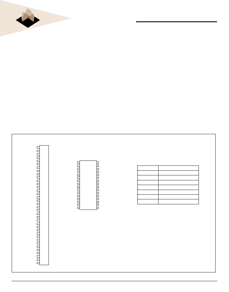
FIG. 1 PIN CONFIGURATIONS
FEATURES
512Kx8 bit CMOS Static
Random Access Memory
∑ Access Times 20 through 100ns
∑ Data Retention Function (EDI8F8512LP)
∑ TTL Compatible Inputs and Outputs
∑ Fully Static, No Clocks
High Density Packaging
∑ 36 Pin SIP, No. 63
∑ 32 Pin DIP, JEDEC Pinout, No. 91 (55-100ns)
∑ 32 Pin DIP, JEDEC Pinout, No. 183 (20-35ns)
Single +5V (±10%) Supply Operation
*This product is subject to change without notice.
The EDI8F8512C is a 4096K bit CMOS Static RAM based on four
128Kx8 or 256Kx4 (high speed) Static RAMs mounted on a multi-
layered epoxy laminate (FR4) substrate.
Functional equivalence to the monolithic four megabit Static RAM
is achieved by utilization of an on-board decoder that interprets the
higher order address(es) to select one of the128Kx8 or 256Kx4 Static
RAMs.
The 32 pin DIP pinout adheres to the JEDEC standard for the four
megabit device, to ensure compatibility with future monolithics.
A low power version with data retention (EDI8F8512LP) is also
available.
All inputs and outputs are TTL compatible and operate from a single
5V supply. Fully asynchronous, the EDI8F8512C requires no clocks
or refreshing for operation.
512Kx8 STATIC RAM CMOS, MODULE
DESCRIPTION
1
2
3
4
5
6
7
8
9
10
11
12
13
14
15
16
17
18
19
20
21
22
23
24
25
26
27
28
29
30
31
32
33
34
35
36
NC
V
CC
W#
DQ2
DQ3
DQ0
A1
A2
A3
A4
V
SS
DQ5
A10
A11
A5
A13
A14
NC
E#
A15
A16
A12
A18
A6
DQ1
V
SS
A0
A7
A8
A9
DQ7
DQ4
DQ6
A17
V
CC
G#
8F8512C Pin Config.
1
2
3
4
5
6
7
8
9
10
11
12
13
14
15
16
A18
A16
A14
A12
A7
A6
A5
A4
A3
A2
A1
A0
DQ0
DQ1
DQ2
V
SS
8F8512C Pin Config
32
31
30
29
28
27
26
25
24
23
22
21
20
19
18
17
V
CC
A15
A17
W#
A13
A8
A9
A11
G#
A10
E#
DQ7
DQ6
DQ5
DQ4
DQ3
PIN NAMES
A0-A18
Address Inputs
E#
Chip Enable
W#
Write Enable
G#
Output Enable
DQ0-DQ7
Common Data Input/Output
V
CC
Power (+5V±10%)
V
SS
Ground
NC
No Connection

EDI8F8512C
2
White Electronic Designs Corporation ∑ (602) 437-1520 ∑ www.wedc.com
White Electronic Designs
July 2002
Rev. 13A
White Electronic Designs Corp. reserves the right to change products or specifications without notice.
DQ0-7
128K x 8
128K x 8
128K x 8
128K x 8
A
0-16
W#
G#
A
17-A18
E#
DECODER
8F8512C Blk Dia
FIG. 2 BLOCK DIAGRAMS
55-100ns
DQ
4-7
256K x 4
256K x 4
256K x 4
256K x 4
A
0-17
W#
G#
A18
E#
DECODER
8F8512C Blk Dia2
DQ0-3
20-35ns

EDI8F8512C
3
White Electronic Designs Corporation ∑ (602) 437-1520 ∑ www.wedc.com
White Electronic Designs
July 2002
Rev. 13A
White Electronic Designs Corp. reserves the right to change products or specifications without notice.
ABSOLUTE MAXIMUM RATINGS*
RECOMMENDED DC OPERATING CONDITIONS
AC TEST CONDITIONS
*Stress greater than those listed under "Absolute Maximum Ratings" may
cause permanent damage to the device. This is a stress rating only and
functional operation of the device at these or any other conditions greater
than those indicated in the operational sections of this specification is not
implied. Exposure to absolute maximum rating conditions for extended
periods may affect reliability.
(Note: For t
EHQZ
, t
GHQZ
and t
WLQZ
, CL = 5pF)
Voltage on any pin relative to V
SS
-0.5V to 7.0V
Operating Temperature T
A
(Ambient)
Commercial
Industrial
0∞C to +70∞C
-40∞C to +85∞C
Storage Temperature
-55∞C to +125∞C
Power Dissipation
4 Watt
Output Current
20 mA
Input Pulse Levels
V
SS
to 3.0V
Input Rise and Fall Times
5ns
Input and Output Timing Levels
1.5V
Output Load 20-35ns
1TTL = 30pF
70-100ns
1TTL, CL = 100pF
Parameter
Sym
Min
Typ
Max
Units
Supply Voltage
V
CC
4.5
5.0
5.5
V
Supply Voltage
V
SS
0
0
0
V
Input High Voltage
V
IH
2.2
≠
6.0
V
Input Low Voltage
V
IL
-0.3
≠
0.8
V
DC ELECTRICAL CHARACTERISTICS
*Typical: T
A
= 25∞C, V
CC
= 5.0V
Parameter
Sym
Conditions
Min
Typ*
Max
Units
35
55 20-25
35
55-100
Operating Power Supply Current
I
CC1
W#, E# = V
IL
, II/O = 0mA, Min Cycle
340
70
570
390
130
mA
Standby (TTL) Power
Supply Current
I
CC2
E# V
IH
, V
IN
V
IL
V
IN
V
IH
DIP
SIP
≠
≠
50
≠
10
≠
85
≠
85
≠
55
65
mA
Full Standby Power
Supply Current (CMOS)
I
CC3
E# V
CC
-0.2V
V
IN
V
CC
-0.2V or
V
IN
0.2V
C
LP
≠
≠
5
≠
2
40
40
≠
40
≠
5
400
mA
µA
Input Leakage Current
I
LI
V
IN
= 0V to V
CC
≠
≠
≠
≠
±10
±10
±10
µA
Output Leakage Current
I
LO
V I/O = 0V to V
CC
≠
≠
≠
≠
±10
±10
±10
µA
Output High Voltage
V
OH
I
OH
= -1.0mA (70), or -4.0 (35)
2.4
≠
≠
≠
≠
≠
≠
V
Output Low Voltage
V
OL
I
OL
= 2.1mA (70), or 8.0mA (35)
≠
≠
≠
≠
0.4
0.4
0.4
V
TRUTH TABLE
CAPACITANCE
(f=1.0MHz, V
IN
=V
CC
or V
SS
)
These parameters are sampled, not 100% tested.
G#
E#
W#
Mode
Output
Power
X
H
X
Standby
HIGH Z
I
CC2
/I
CC3
H
L
H
Output
Deselect
HIGH Z
I
CC1
L
L
H
Read
D
OUT
I
CC1
X
L
L
Write
D
IN
I
CC1
Parameter
Sym
Max
Unit
Address Lines
CI
30
pF
Data Lines
CD/Q
43
pF
Chip Enable Line
CC
10
pF
Write and Output Enable Lines
CW
32
pF

EDI8F8512C
4
White Electronic Designs Corporation ∑ (602) 437-1520 ∑ www.wedc.com
White Electronic Designs
July 2002
Rev. 13A
White Electronic Designs Corp. reserves the right to change products or specifications without notice.
FIG. 3 READ CYCLE 1 - W# HIGH, G#, E# LOW
FIG. 4 READ CYCLE 2 - W# HIGH
ADDRESS 1
ADDRESS 2
t
AVAV
DATA 1
DATA 2
t
AVQV
t
AVQX
8F8512C Rd Cyc1
A
Q
t
GHQZ
t
ELQV
t
ELQX
E#
G#
Q
t
EHQZ
A
t
AVAV
t
GLQV
t
GLQX
t
AVQV
8F8512C Rd Cyc2
AC CHARACTERISTICS READ CYCLE
Parameter
Symbol
20ns
25ns
35ns
Units
JEDEC
Alt.
Min.
Max.
Min.
Max.
Min.
Max.
Read Cycle Time
t
AVAV
t
RC
20
25
35
ns
Address Access Time
t
AVQV
t
AA
20
25
35
ns
Chip Enable Access Time
t
ELQV
t
ACS
20
25
35
ns
Chip Enable to Output in Low Z (1)
t
ELQX
t
CLZ
3
3
3
ns
Chip Disable to Output in High Z
(1)
t
EHQZ
t
CHZ
10
12
15
ns
Output Hold from Address Change
t
AVQX
t
OH
3
3
3
ns
Output Enable to Output Valid
t
GLQV
t
OE
13
15
20
ns
Output Enable to Output in Low Z
(1)
t
GLQX
t
OLZ
0
0
0
ns
Output Disable to Output in High Z (1)
t
GHQZ
t
OHZ
8
10
12
ns
Note: Parameter guaranteed, but not tested.

EDI8F8512C
5
White Electronic Designs Corporation ∑ (602) 437-1520 ∑ www.wedc.com
White Electronic Designs
July 2002
Rev. 13A
White Electronic Designs Corp. reserves the right to change products or specifications without notice.
AC CHARACTERISTICS WRITE CYCLE
Note 1: Parameter guaranteed, but not tested.
Write Cycle
Parameter
Symbol
20ns
25ns
35ns
Units
JEDEC
Alt.
Min
Max
Min
Max
Min
Max
Write Cycle Time
t
AVAV
t
WC
20
25
35
ns
Chip Enable to End of Write
t
ELWH
t
ELEH
t
CW
t
CW
15
15
20
20
30
30
ns
ns
Address Setup Time
t
AVWL
t
AVEL
t
AS
t
AS
0
0
0
0
0
0
ns
ns
Address Valid to End of Write
t
AVWH
t
AVEH
t
AW
t
AW
15
15
20
20
30
30
ns
ns
Write Pulse Width
t
WLWH
t
WLEH
t
WP
t
WP
15
15
20
20
25
25
ns
ns
Write Recovery Time
t
WHAX
t
EHAX
t
WR
TWR
0
0
0
0
0
0
ns
ns
Data Hold Time
t
WHDX
t
EHDX
t
DH
t
DH
3
3
3
3
3
3
ns
ns
Write to Output in High Z (1)
t
WLQZ
t
WHZ
0
10
0
12
0
15
ns
Data to Write Time
t
DVWH
t
DVEH
t
DW
t
DW
12
12
15
15
20
20
ns
ns
Output Active from End of Write (1)
t
WHQX
t
WLZ
3
3
3
ns
AC CHARACTERISTICS READ CYCLE
Note 1: Parameter guaranteed, but not tested.
Symbol
55ns
70ns
85ns
100ns
Parameter
JEDEC
Alt.
Min
Max
Min
Max
Min
Max
Min
Max
Units
Read Cycle Time
t
AVAV
t
RC
55
70
85
100
ns
Address Access Time
t
AVQV
t
AA
55
70
85
100
ns
Chip Enable Access Time
t
ELQV
t
ACS
55
70
85
100
ns
Chip Enable to Output in Low Z (1)
t
ELQX
t
CLZ
5
5
5
5
ns
Chip Disable to Output in High Z (1)
t
EHQZ
t
CHZ
30
30
35
40
ns
Output Hold from Address Change
t
AVQX
t
OH
3
3
3
3
ns
Output Enable to Output Valid
t
GLQV
t
OE
40
40
45
50
ns
Output Enable to Output in Low Z
(1)
t
GLQX
t
OLZ
0
0
0
0
ns
Output Disable to Output in High Z (1)
t
GHQZ
t
OHZ
30
30
35
40
ns

EDI8F8512C
6
White Electronic Designs Corporation ∑ (602) 437-1520 ∑ www.wedc.com
White Electronic Designs
July 2002
Rev. 13A
White Electronic Designs Corp. reserves the right to change products or specifications without notice.
Note 1: Parameter guaranteed, but not tested.
FIG. 7 WRITE CYCLE 1 - W# CONTROLLED
E#
A
t
AVAV
t
ELWH
t
AVWH
t
WLWH
t
AVWL
t
WHAX
W#
HIGH Z
DATA VALID
t
WLQZ
t
WHQX
t
DVWH
t
WHDX
Q
D
8F8512C Write Cyc1
AC CHARACTERISTICS WRITE CYCLE
Parameter
Symbol
55ns
70ns
85ns
100ns
Units
JEDEC
Alt.
Min
Max
Min
Max
Min
Max
Min
Max
Write Cycle Time
t
AVAV
t
WC
55
70
85
100
ns
Chip Enable to End of Write
t
ELWH
t
ELEH
t
CW
t
CW
50
50
65
65
70
70
80
80
ns
ns
Address Setup Time
t
AVWL
t
AVEL
t
AS
t
AS
0
0
0
0
0
0
0
0
ns
ns
Address Valid to End of Write
t
AVWH
t
AVEH
t
AW
t
AW
50
50
65
65
70
70
80
80
ns
ns
Write Pulse Width
t
WLWH
t
WLEH
t
WP
t
WP
50
50
65
65
70
70
80
80
ns
ns
Write Recovery Time
t
WHAX
t
EHAX
t
WR
t
WR
0
0
0
0
0
0
0
0
ns
ns
Data Hold Time
t
WHDX
t
EHDX
t
DH
t
DH
0
0
0
0
0
0
0
0
ns
ns
Write to Output in High Z (1)
t
WLQZ
t
WHZ
0
30
0
30
0
35
0
40
ns
Data to Write Time
t
DVWH
t
DVEH
t
DW
t
DW
30
30
30
30
35
35
40
40
ns
ns
Output Active from End of Write (1)
t
WHQX
t
WLZ
5
5
3
5
ns

EDI8F8512C
7
White Electronic Designs Corporation ∑ (602) 437-1520 ∑ www.wedc.com
White Electronic Designs
July 2002
Rev. 13A
White Electronic Designs Corp. reserves the right to change products or specifications without notice.
FIG. 8 WRITE CYCLE 2 - E# CONTROLLED
A
t
AVEL
HIGH Z
t
AVAV
8F8512C Write Cyc2
t
ELEH
E#
t
AVEH
t
EHAX
W#
t
WLEH
t
EHDX
t
DVEH
Q
DATA VALID
D

EDI8F8512C
8
White Electronic Designs Corporation ∑ (602) 437-1520 ∑ www.wedc.com
White Electronic Designs
July 2002
Rev. 13A
White Electronic Designs Corp. reserves the right to change products or specifications without notice.
LP 70-100ns Only
ORDERING INFORMATION
Standard Power
Speed
(ns)
Package
No.
EDI8F8512C20M6C
20
183
EDI8F8512C25M6C
25
183
EDI8F8512C35M6C
35
183
EDI8F8512C70BSC
70
63
EDI8F8512C85BSC
85
63
EDI8F8512C100BSC
100
63
EDI8F8512C55B6C
55
91
EDI8F8512C70B6C
70
91
EDI8F8512C85B6C
85
91
EDI8F8512C100B6C
100
91
Low Power
with Data Retention
Speed
(ns)
Package
Leads
EDI8F8512LP70BSC
70
63
EDI8F8512LP85BSC
85
63
EDI8F8512LP100BSC
100
63
EDI8F8512LP70B6C
70
91
EDI8F8512LP85B6C
85
91
EDI8F8512LP100B6C
100
91
Note:
To order an Industrial grade product substitute the letter C in the Suffix with
the letter I, e.g., EDI8F8512C70B6C becomes EDI8F8512C70B6I.
FIG. 9 DATA RETENTION E# CONTROLLED
V
CC
t
R
8F8512C Data Retent.
DATA RETENTION MODE
E#
t
CDR
E# V
CC
-0.2V
V
CC
4.5V
4.5V
DATA RETENTION CHARACTERISTICS
*Read Cycle Time
Note: Parameter guaranteed, but not tested.
Characteristic
Sym
Test Conditions
V
CC
Min
Typ
Max
Unit
70∞C 85∞C
Data Retention Voltage
V
CC
V
CC
= 0.2V
2
≠
≠
≠
V
Data Retention Quiescent Current
I
CCDR
E# V
CC
-0.2V
V
IN
V
CC
-0.2V
or V
IN
0.2V
2V
≠
10
125
185
µA
3V
≠
20
200
250
µA
Chip Disable to Data Retention Time (1)
t
CDR
0
≠
≠
≠
ns
Operation Recovery Time (1)
t
R
t
AVAV
*
≠
≠
≠
ns

EDI8F8512C
9
White Electronic Designs Corporation ∑ (602) 437-1520 ∑ www.wedc.com
White Electronic Designs
July 2002
Rev. 13A
White Electronic Designs Corp. reserves the right to change products or specifications without notice.
PACKAGE NO. 63: 36 PIN SINGLE-IN-LINE PACKAGE
PACKAGE DESCRIPTIONS
8F8512C Pkg 2
1.665 MAX.
.085
.065
.175
.125
.025
.015
.620
.590
.248
MAX.
.640
MAX.
NOTE 2
U5
U1
U2
R1
R2
.100 TYP.
15 x .100
1.500 REF.
0.125
Min
4.040 Max.
0.020
0.016
0.575
0.565
0.150
Max
0.100
35 x 0.100 = 3.500
8F8512C Pkg1
ALL DIMENSIONS ARE IN INCHES
8F8512C Pkg3
.010
.005
1.715 MAX.
.640
MAX.
.355
MAX.
1
.175
.125
.620
.590
15 x .100
1.500 REF.
NOT RECOMMENDED FOR NEW DESIGNS
PACKAGE NO. 91: 32 PIN DUAL-IN-LINE PACKAGE
PACKAGE NO. 183: 32 PIN DUAL-IN-LINE PACKAGE