1
White Electronic Designs Corporation (508) 366-5151 www.whiteedc.com
EDI8G322048C
June 2001 Rev. 1
ECO #14323
FEATURES
2048K x 32 bit CMOS Static
Random Access Memory
Access Times: 20, 25, and 35ns
Individual Byte Selects
Fully Static, No Clocks
TTL Compatible I/O
High Density Package
72 lead SIMM, No. 356 (Straight)
Common Data Inputs and Outputs
Single +5V (±10%) Supply Operation
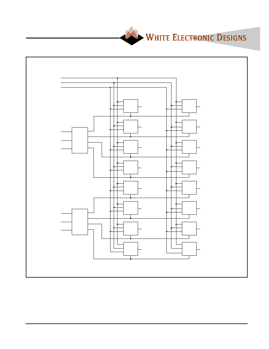
The EDI8G322048C is a high speed 64 megabit Static RAM
module organized as 2048K words by 32 bits. This module is
constructed from sixteen 1024K x 4 Static RAMs in SOJ pack-
ages on an epoxy laminate (FR4) board.
Four chip enables (Eÿ-E3) and the highest order address line are
used to independently enable the four bytes as well as the low
or high block of addressable memory space. Reading or writing
can be executed on individual bytes or any combination of
multiple bytes through proper use of selects.
The EDI8G322048C is offered in a 72 lead SIMM package, which
enables 64 megabits of memory to be placed in less than 1.3
square inches of board space.
All inputs and outputs are TTL compatible and operate from a
single 5V supply. Fully asynchronous circuitry requires no clocks
or refreshing for operation and provides equal access and cycle
times for ease of use.
Pins PD1- PD4, are used to identify module memory density in
applications where alternate modules can be interchanged.
2048K x 32 Static RAM CMOS, High Speed Module
DESCRIPTION
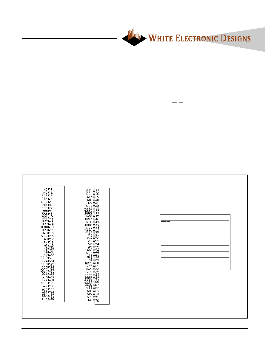
PIN NAMES
Aÿ-A20
Address Inputs
Eÿ-E3
Chip Enables
W
Write Enable
G
Output Enable
DQÿ-DQ31
Common Data
Input/Output
VCC
Power (+5V±10%)
VSS
Ground
NC
No Connection
8G322048C Pin Config.
PIN CONFIGURATION
2
White Electronic Designs Corporation (508) 366-5151 www.whiteedc.com
EDI8G322048C
June 2001 Rev. 1
ECO #14323
DQ0-DQ3
DQ4-DQ7
DQ12-DQ15
DQ24-DQ27
DQ28-DQ31
DQ0-DQ3
DQ4-DQ7
DQ8-DQ11
DQ8-DQ11
DQ16-DQ19
DQ20-DQ23
DQ12-DQ15
DQ16-DQ19
DQ20-DQ23
DQ24-DQ27
DQ28-DQ31
G\
A0-A19
W\
A20
E1\
E2\
A20
E3\
E4\
DECODER
DECODER
U1
1Mx4
U3
1Mx4
1Mx4
U9
1Mx4
U2
1Mx4
U4
1Mx4
1Mx4
1Mx4
U5
1Mx4
1Mx4
U7
1Mx4
1Mx4
U8
1Mx4
1Mx4
U6
1Mx4
1Mx4
U14
U16
U13
U15
U10
U12
U11
8G322048C
BLOCK DIAGRAM
3
White Electronic Designs Corporation (508) 366-5151 www.whiteedc.com
EDI8G322048C
June 2001 Rev. 1
ECO #14323
ABSOLUTE MAXIMUM RATINGS*
RECOMMENDED DC OPERATING CONDITIONS
DC ELECTRICAL CHARACTERISTICS
CAPACITANCE
(f=1.0MHz, VIN=VCC or VSS)
AC TEST CONDITIONS
*Stress greater than those listed under "Absolute Maximum Ratings" may cause
permanent damage to the device. This is a stress rating only and functional operation
of the device at these or any other conditions greater than those indicated in the
operational sections of this specification is not implied. Exposure to absolute
maximum rating conditions for extended periods may affect reliability.
(note: For TEHQZ,TGHQZ and TWLQZ, CL = 5pF)
*Typical: TA = 25∞C, VCC = 5.0V
These parameters are sampled, not 100% tested.
*Each enable controls one byte (x8) within the x32 (doubleword) and one or more byte enables may be driven valid during this
operation.
TRUTH TABLE
Parameter
Sym
Min
Typ
Max
Units
Supply Voltage
VCC
4.5
5.0
5.5
V
Supply Voltage
VSS
0
0
0
V
Input High Voltage
VIH
2.2
--
6.0
V
Input Low Voltage
VIL
-0.3
--
0.8
V
Input Pulse Levels
VSS to 3.0V
Input Rise and Fall Times
5ns
Input and Output Timing Levels
1.5V
Output Load
1TTL, CL = 30pF
Parameter
Sym
Max
Unit
Address Lines
CI
120
pF
Data Lines
CD/Q
20
pF
Chip Enable Line
CC
120
pF
Write Line
CN
120
pF
E0
E1
E2
E3
W
G
Operational Comments
H
H
H
H
H
H
Disabled
L
L
L
L
H
L
Read Double Word
L
L
L
L
L
H
Write Double Word
*
*
*
*
L
H
Write One or More Bytes in Double Word
*
*
*
*
H
L
Read One or More Bytes in Double Word
Parameter
Sym
Conditions
Min
Typ Max Units
Operating Power Supply Current
ICC1
W, E = VIL, II/O = 0mA, Min Cycle
1750
mA
Standby (TTL) Power Supply Current
ICC2
E ≥ VIH, VIN £ VIL or VIN ≥ VIH
800
mA
Full Standby Power Supply Current
ICC3
E ≥ VCC-0.2V
160
mA
CMOS
VIN ≥ VCC-0.2V or VIN £ 0.2V
Input Leakage Current
ILI
VIN = 0V to VCC
--
-- ±80
µA
Output Leakage Current
ILO
V I/O = 0V to VCC
--
-- ±20
µA
Output High Voltage
VOH
IOH = -4.0mA
2.4
--
--
V
Output Low Voltage
VOL
IOL = 8.0mA
--
--
0.4
V
Voltage on any pin relative to VSS
-0.5V to 7.0V
Operating Temperature TA (Ambient)
Commercial
0∞C to +70∞C
Storage Temperature, Plastic
-55∞C to +125∞C
Power Dissipation
7.0 Watts
Output Current
20 mA
4
White Electronic Designs Corporation (508) 366-5151 www.whiteedc.com
EDI8G322048C
June 2001 Rev. 1
ECO #14323
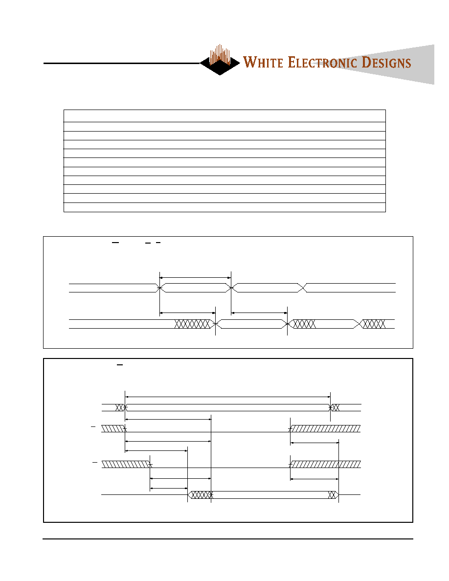
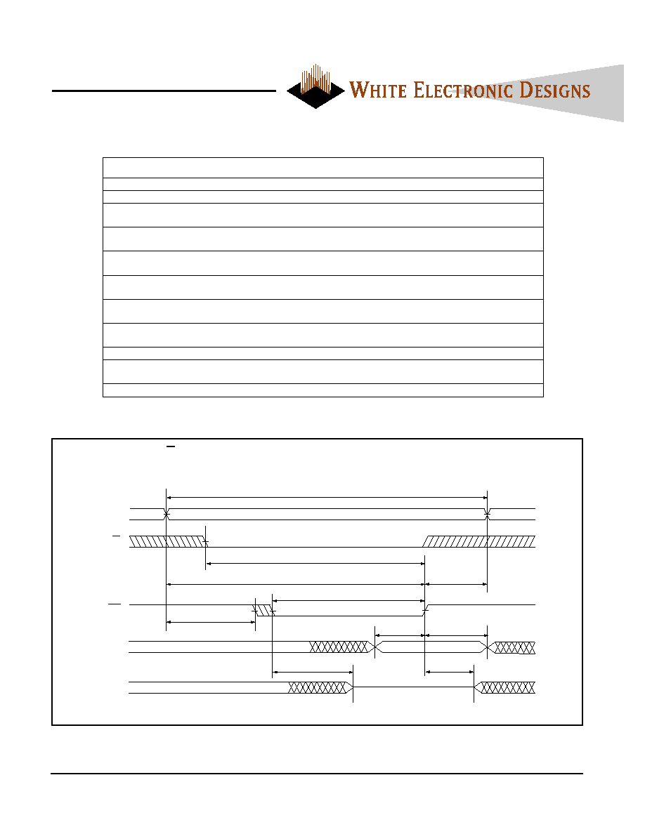
AC CHARACTERISTICS READ CYCLE
READ CYCLE 2 - W HIGH
Note 1: Parameter guaranteed, but not tested.
READ CYCLE 1 - W HIGH, G, E LOW
Symbol
20ns
25ns
35ns
Parameter
JEDEC
Alt.
Min Max
Min
Max
Min
Max Units
Read Cycle Time
TAVAV
TRC
20
25
35
ns
Address Access Time
TAVQV
TAA
20
25
35
ns
Chip Enable Access
TELQV TACS
20
25
35
ns
Chip Enable to Output in Low Z (1)
TELQX TCLZ
3
3
3
ns
Chip Disable to Output in High Z (1)
TEHQZ TCHZ
15
17
20
ns
Output Hold from Address Change
TAVQX TOH
3
3
3
ns
Output Enable to Output Valid
TGLQV TOE
15
17
20
ns
Output Enable to Output in Low Z (1)
TGLQX TOLZ
0
0
0
ns
Output Disable to Output in High Z(1)
TGHQZ TOHZ
15
17
20
ns
ADDRESS 1
ADDRESS 2
TAVAV
DATA 1
DATA 2
TAVQV
TAVQX
8G322048C Rd Cyc1
A
Q
TGHQZ
TELQV
TELQX
E
G
Q
TEHQZ
A
TAVAV
TGLQV
TGLQX
TAVQV
8G322048C Rd Cyc2
5
White Electronic Designs Corporation (508) 366-5151 www.whiteedc.com
EDI8G322048C
June 2001 Rev. 1
ECO #14323
Note 1: Parameter guaranteed, but not tested.
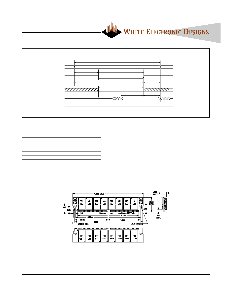
WRITE CYCLE 1 - W CONTROLLED
AC CHARACTERISTICS WRITE CYCLE
Symbol
20ns
25ns
35ns
Parameter
JEDEC
Alt.
Min
Max
Min
Max Min
Max
Units
Write Cycle Time
TAVAV TWC
20
25
35
ns
Chip Enable to End of Write
TELWH TCW
15
20
25
ns
TWLEH TCW
15
20
25
ns
Address Setup Time
TAVWL
TAS
0
0
0
ns
TAVEL
TAS
0
0
0
ns
Address Valid to End of Write
TAVWH TAW
15
20
25
ns
TAVEH TAW
15
20
25
ns
Write Pulse Width
TWLWH TWP
15
20
25
ns
TELEH TWP
15
20
25
ns
Write Recovery Time
TWHAX TWR
0
0
0
ns
TEHAX TWR
0
0
0
ns
Data Hold Time
TWHDX TDH
3
0
0
ns
TEHDX TDH
3
0
0
ns
Write to Output in High Z (1)
TWLQZ TWHZ
0
8
0
12
0
15
ns
Data to Write Time
TDVWH TDW
12
15
20
ns
TDVEH TDW
12
15
20
ns
Output Active from End of Write (1)
TWHQX TWLZ
3
3
3
ns
E
A
TAVAV
TELWH
TAVWH
TWLWH
TAVWL
TWHAX
W
HIGH Z
DATA VALID
TWLQZ
TWHQX
TDVWH
TWHDX
Q
D
8G322048C Write Cyc1
6
White Electronic Designs Corporation (508) 366-5151 www.whiteedc.com
EDI8G322048C
June 2001 Rev. 1
ECO #14323
ORDERING INFORMATION
PACKAGE NO. 407: 72 LEAD SIMM
PACKAGE DESCRIPTIONS
8G322048C Pkg.
WRITE CYCLE 2 - E CONTROLLED
Part Number
Speed
Package
(ns)
No.
EDI8G322048C20MMC
20
407
EDI8G322048C25MMC
25
407
EDI8G322048C35MMC
35
407
A
TAVEL
HIGH Z
TAVAV
8G322048C Write Cyc2
TELEH
E
TAVEH
TEHAX
W
TWLEH
TEHDX
TDVEH
Q
DATA VALID
D
ALL DIMENSIONS ARE IN INCHES