
1
White Electronic Designs Corporation ∑ (602) 437-1520 ∑ www.wedc.com
White Electronic Designs
EDI8L24129V
March 2005
Rev. 5
White Electronic Designs Corp. reserves the right to change products or specifi cations without notice.
128Kx24 SRAM 3.3 Volt
FEATURES
128Kx24 bit CMOS Static
Random Access Memory Array
∑ Fast Access Times: 10, 12, and 15ns
∑ Master Output Enable and Write Control
∑ TTL Compatible Inputs and Outputs
∑ Fully Static, No Clocks
Surface Mount Package
∑ 119 Lead BGA (JEDEC MO-163), No. 391
∑ Small Footprint, 14mm x 22mm
∑ Multiple Ground Pins for Maximum
Noise Immunity
Single +3.3V (±5%) Supply Operation
DSP Memory Solution
Motorola DSP5630xTM
Analog Devices SHARCTM
PIN CONFIGURATION
1
2
3
4
5
6
7
A
NC
AO
A1
A2
A3
A4
NC
B
NC
A5
A6
E#
A7
A8
NC
C
I/012
NC
NC
NC
NC
NC
I/00
D
I/013
V
CC
GND
GND
GND
V
CC
I/01
E
I/014
GND
V
CC
GND
VCC
GND
I/02
F
I/015
V
CC
GND
GND
GND
V
CC
I/03
G
I/016
GND
V
CC
GND
V
CC
GND
I/04
H
I/017
V
CC
GND
GND
GND
V
CC
I/05
I
NC
GND
V
CC
GND
V
CC
GND
NC
J
I/018
V
CC
GND
GND
GND
V
CC
I/06
K
I/019
GND
V
CC
GND
V
CC
GND
I/07
L
I/020
V
CC
GND
GND
GND
V
CC
I/08
M
I/021
GND
V
CC
GND
V
CC
GND
I/09
N
I/022
V
CC
GND
GND
GND
V
CC
I/010
O
I/023
NC
NC
NC
NC
NC
I/011
P
NC
A9
A10
W#
A11
A12
NC
Q
NC
A13
A14
G#
A15
A16
NC
DESCRIPTION
The EDI8L24129VxxBC is a 3.3V, three megabit SRAM
constructed with three 128Kx8 die mounted on a multi-
layer laminate substrate. With 10 to 15ns access times,
x24 width and a 3.3V operating voltage, the EDI8L24129V
is ideal for creating a single chip memory solution for the
Motorola DSP5630x (Figure 3) or a two chip solution for
the Analog Devices SHARCTM DSP (Figure 4).
The single or dual chip memory solutions offer improved
system performance by reducing the length of board traces
and the number of board connections compared to using
multiple monolithic devices. For example, the capacitance
load on the data lines for the BGA package is 58% less
than a monolithic SOJ solution.
The JEDEC Standard 119 lead BGA provides a 44% space
savings over using 128Kx8, 300mil wide SOJs and the BGA
package has a maximum height of 100 mils compared to
148 mils for the SOJ packages. The BGA package also
allows the use of the same manufacturing and inspection
techniques as the Motorola DSP, which is also in a BGA
package.
PIN NAMES
Aÿ-A16
Address Inputs
E#
Chip Enable
W#
Master Write Enable
G#
Master Output Enable
DQÿ-DQ23
Common Data Input/Output
V
CC
Power (3.3V±5%)
GND
Ground
NC
No Connection
2
White Electronic Designs Corporation ∑ (602) 437-1520 ∑ www.wedc.com
White Electronic Designs
EDI8L24129V
March 2005
Rev. 5
White Electronic Designs Corp. reserves the right to change products or specifi cations without notice.
CAPACITANCE
f=1.0MH
Z
, V
IN
=V
CC
or V
SS
Parameter
Sym
Max
Unit
Address Lines
CA
8
pF
Data Lines
CD/Q
10
pF
Write & Output Enable Lines
W#, G#
8
pF
Chip Enable Lines
Eÿ#-E2#
8
pF
These parameters are sampled, not 100% tested.
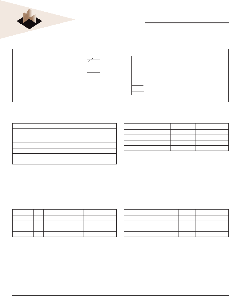
BLOCK DIAGRAM
A
0
-A
16
G#
W#
E#
DQ
0
-DQ
7
DQ
8
-DQ
15
DQ
16
-DQ
23
128K x 24
Memory
Array
17
ABSOLUTE MAXIMUM RATINGS
Voltage on any pin relative to V
SS
-0.5V to 4.6V
Operating Temperature TA (Ambient)
Commercial
Industrial
0∞C to + 70∞C
-40∞C to +85∞C
Storage Temperature
-55∞C to +125∞C
Power Dissipation
1.5 Watts
Output Current.
50 mA
Junction Temperature, TJ
175∞C
* Stress greater than those listed under "Absolute Maximum Ratings" may cause
permanent damage to the device. This is a stress rating only and functional operation
of the device at these or any other conditions greater than those indicated in the
operational sections of this specifi cation is not implied. Exposure to absolute maximum
rating conditions for extended periods may affect reliability.
RECOMMENDED OPERATING CONDITIONS
Parameter
Sym
Min
Typ
Max
Units
Supply Voltage
V
CC
3.135
3.3
3.465
V
Supply Voltage
V
SS
0
0
0
V
Input High Voltage
V
IH
2.2
≠
V
CC
+0.3
V
Input Low Voltage
V
IL
-0.3
≠
0.8
V
TRUTH TABLE
G#
E#
W#
Mode
Output
Power
X
H
X
Standby
High Z
I
CC2
,I
CC3
H
L
H
Output Deselect
High Z
I
CC1
L
L
H
Read
DOUT
I
CC1
X
L
L
Write
DIN
I
CC1

3
White Electronic Designs Corporation ∑ (602) 437-1520 ∑ www.wedc.com
White Electronic Designs
EDI8L24129V
March 2005
Rev. 5
White Electronic Designs Corp. reserves the right to change products or specifi cations without notice.
Parameter
Sym
Conditions
Min
Max
Units
10ns
12-15ns
Operating Power Supply Current
I
CC1
W#= V
IL
, II/O = 0mA,
Min Cycle
420
360
mA
Standby (TTL) Supply Current
I
CC2
E# > V
IH
, V
IN
< V
IL
or
V
IN
> V
IH
, f=ÿMH
Z
90
75
mA
Full Standby CMOS
Supply Current
I
CC3
E# > V
CC
-0.2V
V
IN
> V
CC
-0.2V or
V
IN
< 0.2V
10
10
mA
Input Leakage Current
I
LI
V
IN
= 0V to V
CC
±10
±10
µA
Output Leakage Current
I
LO
V I/O = 0V to V
CC
±10
±10
µA
Output High Volltage
V
OH
I
OH
= -4.0mA
2.4
V
Output Low Voltage
V
OL
I
OL
= 8.0mA
0.4
0.4
V
DC ELECTRICAL CHARACTERISTICS
AC TEST CONDITIONS
Input Pulse Levels
V
SS
to 3.0V
Input Rise and Fall Times
5ns
Input and Output Timing Levels
1.5V
Output Load
Figure 1
(NOTE: For t
EHQZ
,t
GHQZ
and t
WLQZ
, Figure 2)
AC TEST CIRCUIT
D
OUT
30pf
V
L
=1.5V
R
L
= 50
Z0= 50
D
OUT
319W
353
5pf
+3.3V
Figure 1
Figure 2
4
White Electronic Designs Corporation ∑ (602) 437-1520 ∑ www.wedc.com
White Electronic Designs
EDI8L24129V
March 2005
Rev. 5
White Electronic Designs Corp. reserves the right to change products or specifi cations without notice.
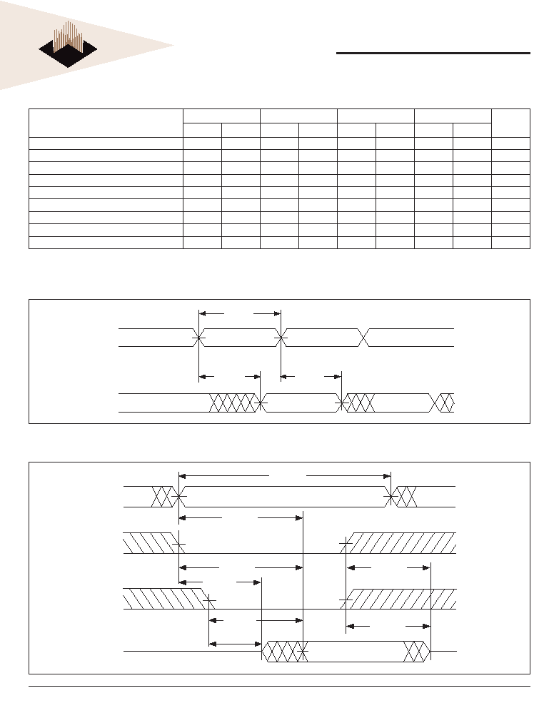
AC CHARACTERISTICS ≠ READ CYCLE
Parameter
Symbol
10ns
12ns
15ns
Units
JEDEC
Alt.
Min Max
Min
Max
Min
Max
Read Cycle Time
t
AVAV
t
RC
10
12
15
ns
Address Access Time
t
AVQV
t
AA
10
12
15
ns
Chip Enable Access Time
t
ELQV
t
ACS
10
12
15
ns
Chip Enable to Output in Low Z (1)
t
ELQX
t
CLZ
3
3
3
ns
Chip Disable to Output in High Z (1)
t
EHQZ
t
CHZ
5
6
7
ns
Output Hold from Address Change
t
AVQX
t
OH
3
3
3
ns
Output Enable to Output Valid
t
GLQV
t
OE
5
6
7
ns
Output Enable to Output in Low Z (1)
t
GLQX
t
OLZ
0
0
0
ns
Output Disable to Output in High Z(1)
t
GHQZ
t
OHZ
5
6
7
ns
Note 1: Parameter guaranteed, but not tested.
READ CYCLE ≠ W# HIGH, G#, E# LOW
A
Q
t
AVQX
t
AVQV
t
AVAV
DATA 2
ADDRESS 1
ADDRESS 2
DATA 1
A
Q
t
AVQV
t
ELQV
t
GLQV
t
ELQX
t
GLQX
t
AVAV
t
EHQZ
t
GHQZ
G#
E#
READ CYCLE 2 ≠ W# HIGH
5
White Electronic Designs Corporation ∑ (602) 437-1520 ∑ www.wedc.com
White Electronic Designs
EDI8L24129V
March 2005
Rev. 5
White Electronic Designs Corp. reserves the right to change products or specifi cations without notice.
AC CHARACTERISTICS ≠ WRITE CYCLE
Parameter
Symbol
10ns
12ns
15ns
Units
JEDEC
Alt.
Min
Max
Min
Max
Min
Max
Write Cycle Time
t
AVAV
t
WC
10
12
15
ns
Chip Enable to End of Write
t
ELWH
t
ELEH
t
CW
t
CW
8
8
9
9
9
9
ns
ns
Address Setup Time
t
AVWL
t
AVEL
t
AS
t
AS
0
0
0
0
0
0
ns
ns
Address Valid to End of Write
t
AVWH
t
AVEH
t
AW
t
AW
8
8
9
9
10
10
ns
ns
Write Pulse Width
t
WLWH
t
WLEH
t
WP
t
WP
8
8
10
10
11
11
ns
ns
Write Recovery Time
t
WHAX
t
EHAX
t
WR
t
WR
0
0
0
0
0
0
ns
ns
Data Hold Time
t
WHDX
t
EHDX
t
DH
t
DH
0
0
0
0
0
0
ns
ns
Write to Output in High Z (1)
t
WLQZ
t
WHZ
0
5
0
6
0
7
ns
Data to Write Time
t
DVWH
t
DVEH
t
DW
t
DW
6
6
6
6
7
7
ns
ns
Output Active from End of Write (1)
t
WHQX
t
WLZ
3
3
3
ns
Note 1: Parameter guaranteed, but not tested.
WRITE CYCLE ≠ W# CONTROLLED
A
D
t
AVWH
t
ELWH
t
WHAX
t
WLWH
t
DVWH
t
WLQZ
t
WHQX
t
AVWL
t
WHDX
t
AVAV
DATA VALID
HIGH Z
W#
E#
Q
6
White Electronic Designs Corporation ∑ (602) 437-1520 ∑ www.wedc.com
White Electronic Designs
EDI8L24129V
March 2005
Rev. 5
White Electronic Designs Corp. reserves the right to change products or specifi cations without notice.
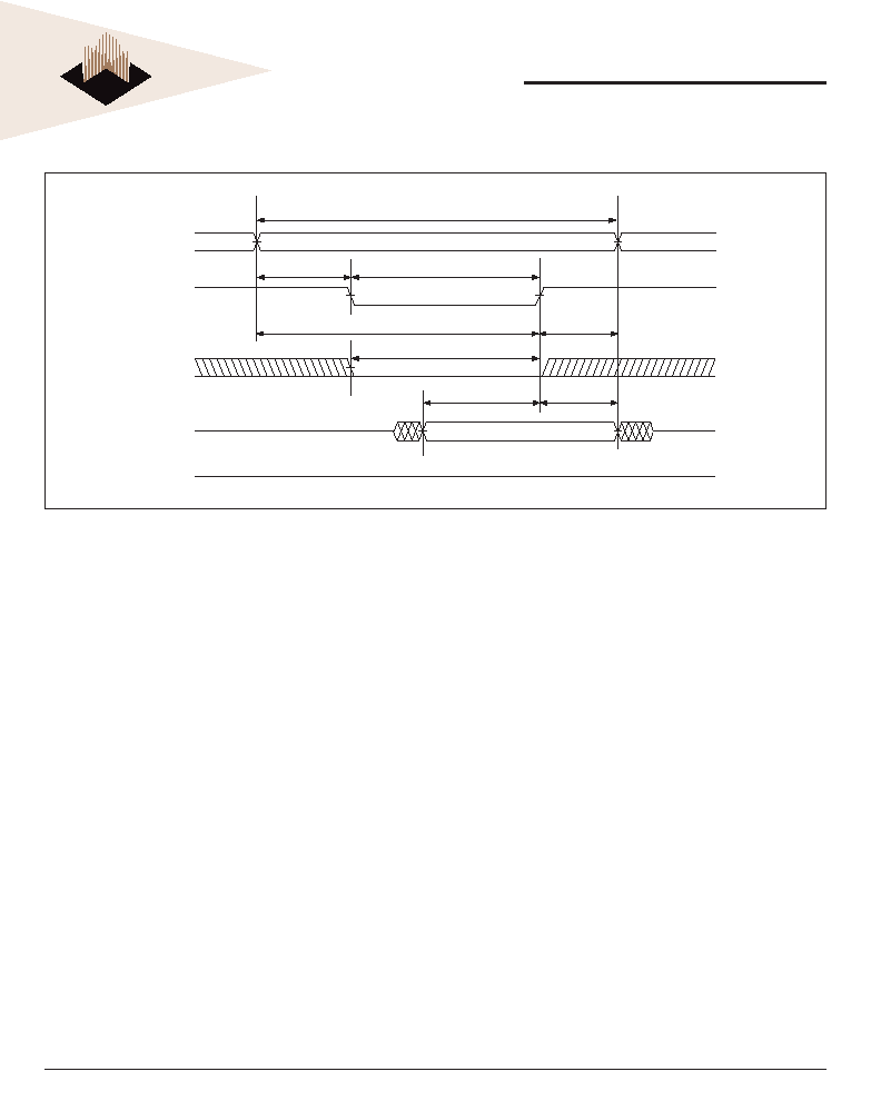
WRITE CYCLE 2 ≠ E# CONTROLLED
A
W#
E#
D
Q
t
AVAV
t
AVEL
t
EHAX
t
DVEH
t
EHDX
t
ELEH
t
AVEH
DATA VALID
HIGH Z
t
WLEH

7
White Electronic Designs Corporation ∑ (602) 437-1520 ∑ www.wedc.com
White Electronic Designs
EDI8L24129V
March 2005
Rev. 5
White Electronic Designs Corp. reserves the right to change products or specifi cations without notice.
Package No. 391
119 Lead BGA
JEDEC MO-163
PACKAGE DESCRIPTION
Industrial (-40∞C to +85∞C)
Part Number
Speed
(ns)
Package
No.
EDI8L24129V10BI
10
391
EDI8L24129V12BI
12
391
EDI8L24129V15BI
15
391
Commercial (0∞C to +70∞C)
Part Number
Speed
(ns)
Package
No.
EDI8L24129V10BC
10
391
EDI8L24129V12BC
12
391
EDI8L24129V15BC
15
391
ORDERING INFORMATION
0.300
BSC
0.800
BSC
0.866
BSC
PIN 1
INDEX
0.050
TYP
0.551
BSC
0.028
MAX.
0.060 NOM./0.110 MAX.

8
White Electronic Designs Corporation ∑ (602) 437-1520 ∑ www.wedc.com
White Electronic Designs
EDI8L24129V
March 2005
Rev. 5
White Electronic Designs Corp. reserves the right to change products or specifi cations without notice.
FIGURE 3 ≠ INTERFACING THE MOTOROLA DSP5630X DSP FAMILY
WITH THE EDI8L24129V (128KX24)
FIGURE 4 ≠ INTERFACING THE 21060L OR THE 21062L TO THE EDI8L24129V, 119 BGA
(CREATING A 128KX48 MEMORY ARRAY)
Address Bus
A23-0
Databus
D23-0
Motorola
DSP5630x
EDI8L24129V
(128K x 24)
A16-0
E#
W#
G#
DQ0-23
EDI8L24129V
(128K x 24)
A16-0
E#
W#
G#
DQ0-23
EDI8L24129V
(128K x 24)
A16-0
E#
W#
G#
DQ0-23
AA0
AA1
AA2
AA3
WR#
RD#
Address Bus
A31-0
Databus
D47-0
Analog
ADSP-2106xL
EDI8L24129V
(128K x 24)
MSX#
WR#
RD#
A16-0
E#
W#
G#
DQ16-23
DQ8-15
DQ0-7
EDI8L24129V
(128K x 24)
A16-0
E#
W#
G#
DQ16-23
DQ8-15
DQ0-7
NOTES:
1.
In this example three 128K x 24 external memory arrays are shown, one for X data, one for Y data and one for Program. Specifi c
applications may require one, two or all three arrays.
2.
Any combination of AA0-AA3 may be used as chip selects. However, each chip select may only be used to select one memory array.