1
White Electronic Designs Corporation (508) 366-5151 www.whiteedc.com
White Electronic Designs
EDI8L24129V
1
2
3
4
5
6
7
A
NC
AO
A1
A2
A3
A4
NC
B
NC
A5
A6
E
A7
A8
NC
C
I/012
NC
NC
NC
NC
NC
I/00
D
I/013
VCC
GND
GND
GND
VCC
I/01
E
I/014
GND
VCC
GND
VCC
GND
I/02
F
I/015
VCC
GND
GND
GND
VCC
I/03
G
I/016
GND
VCC
GND
VCC
GND
I/04
H
I/017
VCC
GND
GND
GND
VCC
I/05
I
NC
GND
VCC
GND
VCC
GND
NC
J
I/018
VCC
GND
GND
GND
VCC
I/06
K
I/019
GND
VCC
GND
VCC
GND
I/07
L
I/020
VCC
GND
GND
GND
VCC
I/08
M
I/021
GND
VCC
GND
VCC
GND
I/09
N
I/022
VCC
GND
GND
GND
VCC
I/010
O
I/023
NC
NC
NC
NC
NC
I/011
P
NC
A9
A10
W
A11
A12
NC
Q
NC
A13
A14
G
A15
A16
NC
128Kx24 SRAM 3.3 Volt
FEATURES
128Kx24 bit CMOS Static
Random Access Memory Array
< Fast Access Times: 10, 12, and 15ns
< Master Output Enable and Write Control
< TTL Compatible Inputs and Outputs
< Fully Static, No Clocks
Surface Mount Package
< 119 Lead BGA (JEDEC MO-163), No. 391
< Small Footprint, 14mm x 22mm
< Multiple Ground Pins for Maximum
Noise Immunity
Single +3.3V (�5%) Supply Operation
DSP Memory Solution
< Motorola DSP5630xTM
< Analog Devices SHARCTM
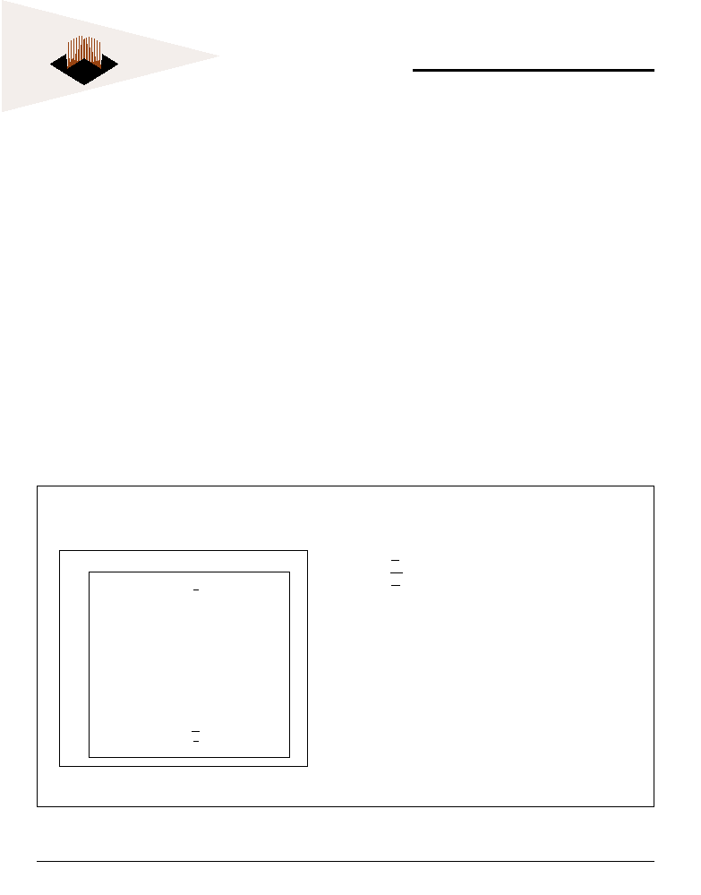
PIN CONFIGURATION
Pin Symbols
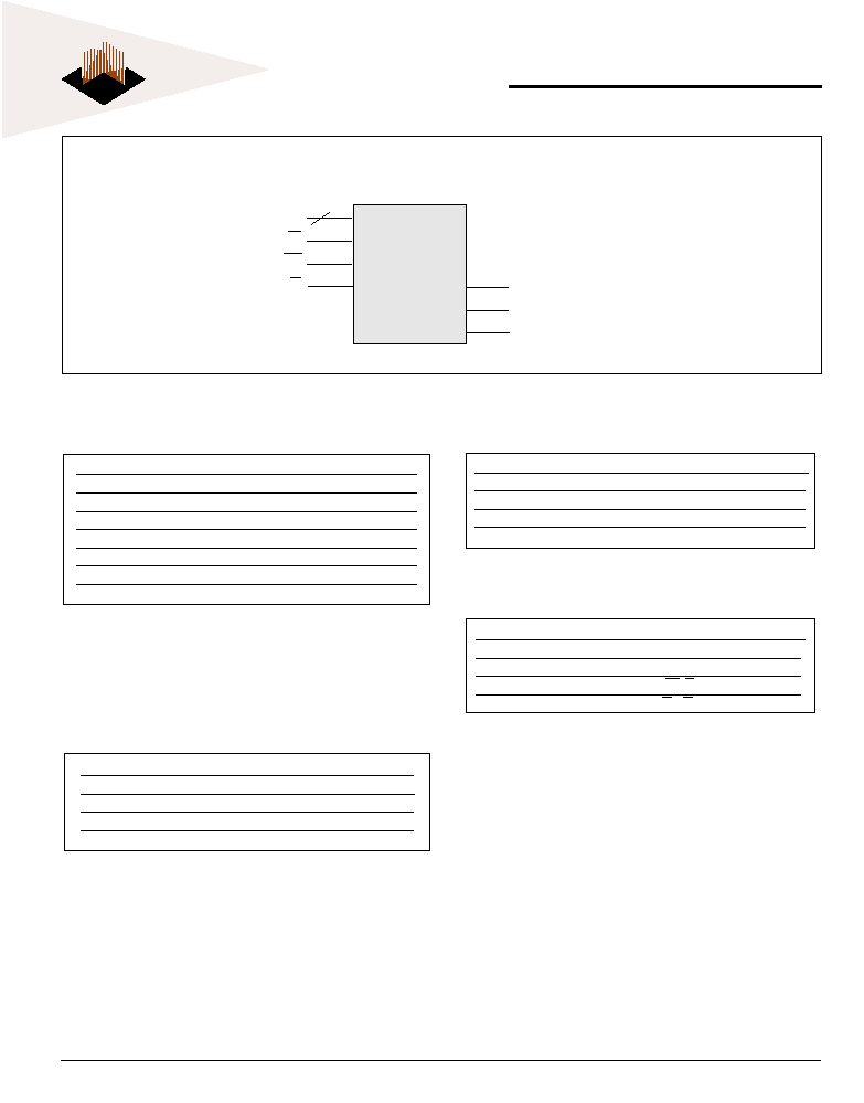
The EDI8L24129VxxBC is a 3.3V, three megabit SRAM
constructed with three 128Kx8 die mounted on a multi-
layer laminate substrate. With 10 to 15ns access times,
x24 width and a 3.3V operating voltage, the
EDI8L24129V is ideal for creating a single chip memory
solution for the Motorola DSP5630x (Figure 3) or a two
chip solution for the Analog Devices SHARCTM DSP
(Figure 4).
The single or dual chip memory solutions offer improved
system performance by reducing the length of board
traces and the number of board connections compared
to using multiple monolithic devices. For example, the
capacitance load on the data lines for the BGA package
is 58% less than a monolithic SOJ solution.
The JEDEC Standard 119 lead BGA provides a 44%
space savings over using 128Kx8, 300mil wide SOJs
and the BGA package has a maximum height of 100
mils compared to 148 mils for the SOJ packages. The
BGA package also allows the use of the same manu-
facturing and inspection techniques as the Motorola
DSP, which is also in a BGA package.
Pin Names
A�-A16
Address Inputs
E
Chip Enable
W
Master Write Enable
G
Master Output Enable
DQ�-DQ23
Common Data Input/Output
VCC
Power (3.3V�5%)
GND
Ground
NC
No Connection
July 2002 Rev 3
ECO #14690
2
White Electronic Designs Corporation Westborough MA (508) 366-5151
White Electronic Designs
EDI8L24129V
Parameter
Sym
Max
Unit
Address Lines
CA
8
pF
Data Lines
CD/Q
10
pF
Write & Output Enable Lines
W, G
8
pF
Chip Enable Lines
E�-E2
8
pF
A
BSOLUTE
M
AXIMUM
R
ATINGS
R
ECOMMENDED
O
PERATING
C
ONDITIONS
C
APACITANCE
BLOCK DIAGRAM
A
0
-A
16
G
W
E
DQ
0
-DQ
7
DQ
8
-DQ
15
DQ
16
-DQ
23
128K x 24
Memory
Array
17
*Stress greater than those listed under "Absolute Maximum Ratings"
may cause permanent damage to the device. This is a stress rating
only and functional operation of the device at these or any other
conditions greater than those indicated in the operational sections of
this specification is not implied. Exposure to absolute maximum rating
conditions for extended periods may affect reliability.
Voltage on any pin relative to VSS
-0.5V to 4.6V
Operating Temperature TA (Ambient)
Commercial
0�C to + 70�C
Industrial
-40�C to +85�C
Storage Temperature
-55�C to +125�C
Power Dissipation
1.5 Watts
Output Current.
50 mA
Junction Temperature, TJ
175�C
Parameter
Sym
Min Typ
Max
Units
Supply Voltage
VCC 3.135 3.3
3.465
V
Supply Voltage
VSS
0
0
0
V
Input High Voltage
VIH
2.2
VCC+0.3 V
Input Low Voltage
VIL
-0.3
0.8
V
(f=1.0MHz, V
IN
=V
CC
or V
SS
)
These parameters are sampled, not 100% tested.
G
E
W
Mode
Output
Power
X
H
X
Standby
High Z
ICC2,ICC3
H
L
H Output Deselect
High Z
ICC1
L
L
H
Read
DOUT
ICC1
X
L
L
Write
DIN
ICC1
T
RUTH
T
ABLE
3
White Electronic Designs Corporation (508) 366-5151 www.whiteedc.com
White Electronic Designs
EDI8L24129V
Parameter
Sym
Conditions
Min
Max
Units
10ns
12-15ns
ns
Operating Power Supply Current
ICC1
W= VIL, II/O = 0mA,
420
360
mA
Min Cycle
Standby (TTL) Supply Current
ICC2
E > VIH, VIN < VIL or
90
75
mA
VIN > VIH, f=�MHz
Full Standby CMOS
ICC3
E > VCC-0.2V
10
10
mA
Supply Current
VIN > VCC-0.2V or
VIN < 0.2V
Input Leakage Current
ILI
VIN = 0V to VCC
�10
�10
�A
Output Leakage Current
ILO
V I/O = 0V to VCC
�10
�10
�A
Output High Volltage
VOH
IOH = -4.0mA
2.4
V
Output Low Voltage
VOL
IOL = 8.0mA
0.4
0.4
V
DC E
LECTRICAL
C
HARACTERISTICS
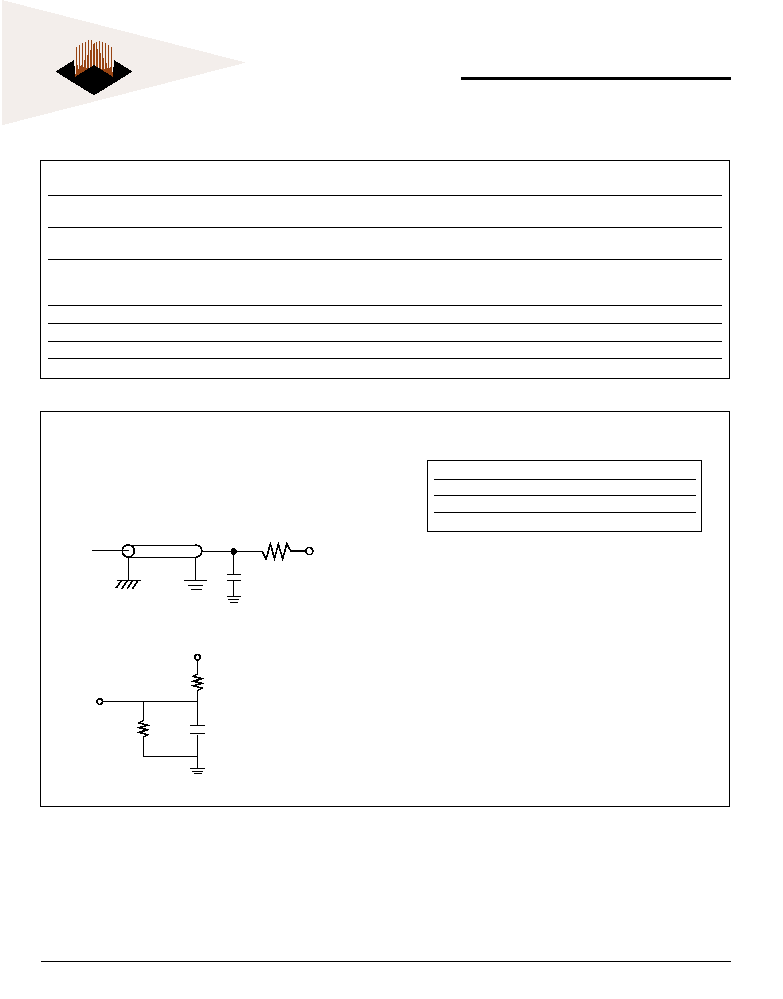
AC T
EST
C
ONDITIONS
AC T
EST
C
IRCUIT
(NOTE: For TEHQZ,TGHQZ and TWLQZ, Figure 2)
Input Pulse Levels
VSS to 3.0V
Input Rise and Fall Times
5ns
Input and Output Timing Levels
1.5V
Output Load
Figure 1
D
OUT
30pf
V
L
=1.5V
R
L
= 50
Z
0
= 50
D
OUT
319
353
5pf
+3.3V
FIG. 1
FIG. 2

4
White Electronic Designs Corporation Westborough MA (508) 366-5151
White Electronic Designs
EDI8L24129V
Symbol
10ns
12ns
15ns
Parameter
JEDEC
Alt.
Min
Max
Min
Max
Min
Max
Units
Read Cycle Time
TAVAV
TRC
10
12
15
ns
Address Access Time
TAVQV
TAA
10
12
15
ns
Chip Enable Access Time
TELQV
TACS
10
12
15
ns
Chip Enable to Output in Low Z (1)
TELQX
TCLZ
3
3
3
ns
Chip Disable to Output in High Z (1)
TEHQZ
TCHZ
5
6
7
ns
Output Hold from Address Change
TAVQX
TOH
3
3
3
ns
Output Enable to Output Valid
TGLQV
TOE
5
6
7
ns
Output Enable to Output in Low Z (1)
TGLQX
TOLZ
0
0
0
ns
Output Disable to Output in High Z(1)
TGHQZ
TOHZ
5
6
7
ns
Note 1: Parameter guaranteed, but not tested.
AC C
HARACTERISTICS
- R
EAD
C
YCLE
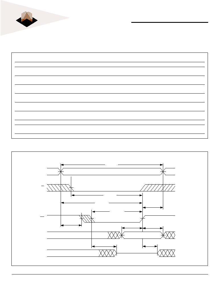
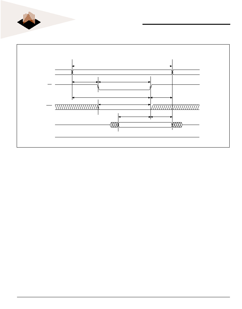
READ CYCLE - W HIGH, G, E LOW
A
Q
t
AVQX
t
AVQV
t
AVAV
DATA 2
ADDRESS 1
ADDRESS 2
DATA 1
A
Q
t
AVQV
t
ELQV
t
GLQV
t
ELQX
t
GLQX
t
AVAV
t
EHQZ
t
GHQZ
G
E
READ CYCLE 2 - W HIGH
5
White Electronic Designs Corporation (508) 366-5151 www.whiteedc.com
White Electronic Designs
EDI8L24129V
Note 1: Parameter guaranteed, but not tested.
Symbol
10ns
12ns
15ns
Parameter
JEDEC
Alt.
Min
Max
Min
Max
Min
Max
Units
Write Cycle Time
TAVAV
TWC
10
12
15
ns
Chip Enable to End of Write
TELWH
TCW
8
9
9
ns
TELEH
TCW
8
9
9
ns
Address Setup Time
TAVWL
TAS
0
0
0
ns
TAVEL
TAS
0
0
0
ns
Address Valid to End of Write
TAVWH
TAW
8
9
10
ns
TAVEH
TAW
8
9
10
ns
Write Pulse Width
TWLWH
TWP
8
10
11
ns
TWLEH
TWP
8
10
11
ns
Write Recovery Time
TWHAX
TWR
0
0
0
ns
TEHAX
TWR
0
0
0
ns
Data Hold Time
TWHDX
TDH
0
0
0
ns
TEHDX
TDH
0
0
0
ns
Write to Output in High Z (1)
TWLQZ
TWHZ
0
5
0
6
0
7
ns
Data to Write Time
TDVWH
TDW
6
6
7
ns
TDVEH
TDW
6
6
7
ns
Output Active from End of Write (1)
TWHQX
TWLZ
3
3
3
ns
AC C
HARACTERISTICS
- W
RITE
CYCLE
WRITE CYCLE - W CONTROLLED
A
D
t
AVWH
t
ELWH
t
WHAX
t
WLWH
t
DVWH
t
WLQZ
t
WHQX
t
AVWL
t
WHDX
t
AVAV
DATA VALID
HIGH Z
W
E
Q
6
White Electronic Designs Corporation Westborough MA (508) 366-5151
White Electronic Designs
EDI8L24129V
WRITE CYCLE 2 - E CONTROLLED
A
W
E
D
Q
t
AVAV
t
AVEL
t
EHAX
t
DVEH
t
EHDX
t
ELEH
t
AVEH
DATA VALID
HIGH Z
t
WLEH
7
White Electronic Designs Corporation (508) 366-5151 www.whiteedc.com
White Electronic Designs
EDI8L24129V
Part Number
Speed
Package
(ns)
No.
EDI8L24129V12BI
12
391
EDI8L24129V15BI
15
391
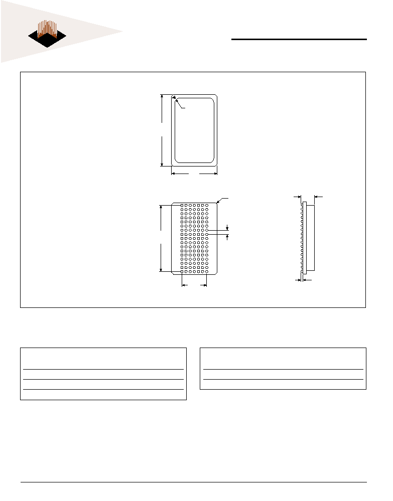
PACKAGE NO. 391
119 LEAD BGA
JEDEC MO-163
PACKAGE DESCRIPTION
Part Number
Speed
Package
(ns)
No.
EDI8L24129V10BC
10
391
EDI8L24129V12BC
12
391
EDI8L24129V15BC
15
391
O
RDERING
I
NFORMATION
C
OMMERCIAL
(0�C
TO
+70�C)
I
NDUSTRIAL
(-40�C
TO
+85�C)
0.300
BSC
0.800
BSC
0.866
BSC
PIN 1
INDEX
R.060 MAX
(4x)
0.050
TYP
0.551
BSC
0.028
MAX.
0.110
MAX.

8
White Electronic Designs Corporation Westborough MA (508) 366-5151
White Electronic Designs
EDI8L24129V
FIG. 3 INTERFACING THE MOTOROLA DSP5630X DSP FAMILY
WITH THE EDI8L24129V (128KX24)
FIG. 4 INTERFACING THE 21060L OR THE 21062L TO THE
EDI8L24129V, 119 BGA (CREATING A 128KX48 MEMORY ARRAY)
Address Bus
A
23-0
Databus
D
23-0
Motorola
DSP5630x
EDI8L24129V
(128K x 24)
AA
0
AA
1
AA
2
AA
3
WR
RD
A
16-0
E
W
G
DQ
0-23
EDI8L24129V
(128K x 24)
A
16-0
E
W
G
DQ
0-23
EDI8L24129V
(128K x 24)
A
16-0
E
W
G
DQ
0-23
Address Bus
A
31-0
Databus
D
47-0
Analog
ADSP-2106xL
EDI8L24129V
(128K x 24)
MS
X
WR
RD
A
16-0
E
W
G
DQ
16-23
DQ
8-15
DQ
0-7
EDI8L24129V
(128K x 24)
A
16-0
E
W
G
DQ
16-23
DQ
8-15
DQ
0-7
NOTES:
1. In this example three 128K x 24 external memory arrays are shown, one for X data, one for Y data and one for Program. Specific
applications may require one, two or all three arrays.
2. Any combination of AA
0
-AA
3
may be used as chip selects. However, each chip select may only be used to select one memory array.