
1
White Electronic Designs Corporation ∑ Westborough, MA 01581 ∑
(508) 366-5151 www.whiteedc.com
EDI8L32256V
NOT
R
ECOMMENDED
FOR
N
EW
DESIGN
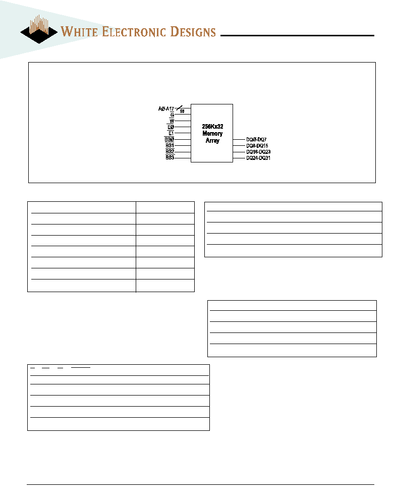
256Kx32 SRAM
FEATURES
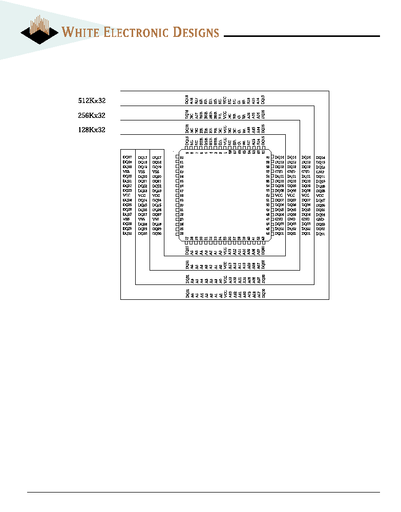
PIN CONFIGURATIONS
PIN DESCRIPTION
n 256Kx32 bit CMOS Static
n DSP Memory Solution
∑ ADSP - 21060L (SHARC)
∑ ADSP - 21062L (SHARC)
∑ TMS320LC31
n Random Access Memory Array
∑ Fast Access Times: 12, 15, 17 and 20ns
∑ Individual Byte Enables
∑ User Configurable Organization
with Minimal Additional Logic
∑ Master Output Enable and Write Control
∑ TTL Compatible Inputs and Outputs
∑ Fully Static, No Clocks
n Surface Mount Package
∑ 68 Lead PLCC, No. 99 JEDEC MO-47AE
∑ Small Footprint, 0.990 Sq. In.
∑ Multiple Ground Pins for Maximum Noise Immunity
n Single 3.3V (±5%) Supply Operation
The EDI8L32256V is a high speed, 3.3 volt, 8 megabit SRAM.
The device is available with access times of 12, 15, 17 and
20ns, allowing the creation of a no wait state DSP memory
solution.
The device can be configured as a 256Kx32 and used to
create a single chip external data memory solution for Texas
Instruments' TMS320LC31 (figure 3), or Analog Device's
SHARC
TM
DSP (figure 4).
Alternatively the device's chip enables can be used to con-
figure it as a 512Kx16. A 512Kx48 program memory array
for Analog's SHARC DSP is created using three devices (fig-
ure 5). If this memor y is too deep, two 256Kx24s
(EDI8L24256V) can be used to create a 256Kx48 array or
two 128Kx24s (EDI8L24128V) can be used to create a
128Kx48 array.
The device provides a 32% space savings when compared
to two monolithic 256Kx16, 44 pin SOJs.
The device provides a memory upgrade of the EDI8L32128V
(128Kx32). For more memory the device can be upgraded
to the EDI8L32512V (512Kx32). For additional upgrade in-
formation see figure 6.
NOTE: Solder Reflow temperature should not exceed 260∞C for 10 seconds.
Aÿ-A17
Address Inputs
Eÿ-E1
Chip Enables (One per Word)
BSÿ-BS3
Byte Selects (One per Byte)
W
Master Write Enable
G
Master Output Enable
DQÿ-DQ31
Common Data Input/Output
VCC
Power (3.3V±5%)
VSS
Ground
NC
No Connection
March, 1998 Rev. 2
ECO# 10135
2
White Electronic Designs Corporation ∑ Westborough, MA 01581 ∑
(508) 366-5151 www.whiteedc.com
EDI8L32256V
ABSOLUTE MAXIMUM RATINGS
RECOMMENDED OPERATING CONDITIONS
CAPACITANCE
(F=1.0MHZ, VIN=VCC OR VSS)
BLOCK DIAGRAM
TRUTH TABLE
Parameter
Sym
Min
Typ
Max
Units
Supply Voltage
VCC
3.135
3.3
3.465
V
Supply Voltage
VSS
0
0
0
V
Input High Voltage
VIH
2.2
- -
VCC+0.3
V
Input Low Voltage
VIL
-0.3
- -
0.8
V
Voltage on any pin relative to VSS
-0.5V to 4.6V
Operating Temperature TA (Ambient)
Commercial
0∞C to + 70∞C
Industrial
-40∞C to +85∞C
Storage Temperature
-55∞C to +125∞C
Power Dissipation
1.7 Watts
Output Current.
20 mA
Junction Temperature, TJ
175∞C
Parameter
Sym
Max
Unit
Address Lines
CA
20
p F
Data Lines
CD/Q
10
p F
Write & Output Enable Lines
W, G
6
p F
Chip Enable Lines/Byte Select
E, BS
9
p F
E
W
G
BSÿ-3
Mode
Output
Power
H
X
X
X
Standby
High Z
ICC2,ICC3
L
H
H
X
Output Disable
High Z
ICC1
L
X
X
H
Output Disable
High Z
ICC1
L
H
L
L
Read
DOUT
ICC1
L
L
X
L
Write
DIN
ICC1
*Stress greater than those listed under "Absolute Maximum Ratings" may cause
permanent damage to the device. This is a stress rating only and functional
operation of the device at these or any other conditions greater than those
indicated in the operational sections of this specification is not implied.
Exposure to absolute maximum rating conditions for extended periods may
affect reliability.
X Means Don't Care

3
White Electronic Designs Corporation ∑ Westborough, MA 01581 ∑
(508) 366-5151 www.whiteedc.com
EDI8L32256V
DC ELECTRICAL CHARACTERISTICS
AC TEST CIRCUIT
AC TEST CONDITIONS
(note: For TEHQZ,TGHQZ and TWLQZ, see figure 2)
Input Pulse Levels
VSS to 3.0V
Input Rise and Fall Times
5ns
Input and Output Timing Levels
1.5V
Output Load
Figure 1
Parameter
Sym
Conditions
Min
Max
Units
12/15
17/20
ns
Operating Power Supply Current
ICC1
W= VIL, II/O = 0mA,
480
440
mA
Min Cycle
Standby (TTL) Supply Current
ICC2
E
≥ VIH, VIN £ VIL or
100
100
mA
VIN
≥ VIH, f=ÿMHz
Full StandbySupply Current
ICC3
E
≥ VCC-0.2V
20
20
mA
VIN
≥ VCC-0.2V or
VIN
£ 0.2V
Input Leakage Current
ILI
VIN = 0V to VCC
±10
±10
µA
Output Leakage Current
ILO
V I/O = 0V to VCC
±10
±10
µA
Output High Volltage
VOH
IOH = -4.0mA
2.4
V
Output Low Voltage
VOL
IOL = 8.0mA
0.4
0.4
V

4
White Electronic Designs Corporation ∑ Westborough, MA 01581 ∑
(508) 366-5151 www.whiteedc.com
EDI8L32256V
AC CHARACTERISTICS - READ CYCLE
READ CYCLE 2 - W HIGH
READ CYCLE 1 - W HIGH, G, E LOW
Symbol
12ns
15ns
17ns
20ns
Parameter
JEDEC
Alt.
Min
Max
Min
Max
Min
Max
Min
Max
Units
Read Cycle Time
TAVAV
TRC
12
15
17
20
ns
Address Access Time
TAVQV
TAA
12
15
17
20
ns
Chip Enable Access Time
TELQV
TACS
12
15
17
20
ns
Byte Select Access Time
TBLQX
TBLZ
12
15
17
20
ns
Chip Enable to Output in Low Z (1)
TELQX
TCLZ
3
3
3
3
ns
Byte Select to Output in Low Z
TBLQX
TBLZ
3
3
3
3
ns
Chip Disable to Output in High Z (1)
TEHQZ
TCHZ
7
8
8
10
ns
Byte Select to Output in High Z
TBHQZ
TBHZ
7
8
8
10
ns
Output Hold from Address Change
TAVQX
TOH
3
3
3
3
ns
Output Enable to Output Valid
TGLQV
TOE
5
6
8
10
ns
Output Enable to Output in Low Z (1)
TGLQX
TOLZ
2
2
2
2
ns
Output Disable to Output in High Z(1)
TGHQZ
TOHZ
4
5
6
8
ns

5
White Electronic Designs Corporation ∑ Westborough, MA 01581 ∑
(508) 366-5151 www.whiteedc.com
EDI8L32256V
AC CHARACTERTISTICS - WRITE CYCLE
Symbol
12ns
15ns
17ns
20ns
Parameter
JEDEC
Alt.
Min
Max
Min
Max
Min
Max
Min
Max
Units
Write Cycle Time
TAVAV
TWC
12
15
17
20
ns
Chip Enable to End of Write
TELWH
TCW
8
12
10
15
ns
TELEH
TCW
8
12
10
15
ns
Byte Select to End of Write
TBLWH
TBW
8
12
10
15
ns
Address Setup Time
TAVWL
TAS
0
0
0
0
ns
TAVEL
TAS
0
0
0
0
ns
Address Valid to End of Write
TAVWH
TAW
9
12
12
15
ns
TAVEH
TAW
9
12
12
15
ns
Write Pulse Width
TWLWH
TWP
9
12
12
15
ns
TWLEH
TWP
9
12
12
15
ns
Write Recovery Time
TWHAX
TWR
0
0
0
0
ns
TEHAX
TWR
0
0
0
0
ns
Data Hold Time
TWHDX
TDH
0
0
0
0
ns
TEHDX
TDH
0
0
0
0
ns
Write to Output in High Z (1)
TWLQZ
TWHZ
0
5
0
6
0
7
0
7
ns
Data to Write Time
TDVWH
TDW
5
8
8
10
ns
TDVEH
TDW
5
8
8
10
ns
Output Active from End of Write (1)
TWHQX
TWLZ
2
2
2
2
ns
Note 1: Parameter guaranteed, but not tested.
Write Cycle 1 - W Controlled

6
White Electronic Designs Corporation ∑ Westborough, MA 01581 ∑
(508) 366-5151 www.whiteedc.com
EDI8L32256V
WRITE CYCLE 2 - E CONTROLLED

7
White Electronic Designs Corporation ∑ Westborough, MA 01581 ∑
(508) 366-5151 www.whiteedc.com
EDI8L32256V
NOT
RECOMMENDED
FOR
N
EW
DESIGN
PACKAGE DESCRIPTION
ORDERING INFORMATION
Weight = 4.2g
Theta J
A
= 40∞C/W
Theta J
c
= 15∞C/W
Part Number
Speed
Package
(ns)
No.
EDI8L32256V12AC
12
99
EDI8L32256V15AC
15
99
EDI8L32256V17AC
17
99
EDI8L32256V20AC
20
99
COMMERCIAL (0∞C TO 70∞C)
INDUSTRIAL (-40∞C TO +85∞C)
Part Number
Speed
Package
(ns)
No.
EDI8L32256V15AI
15
99
EDI8L32256V17AI
17
99
EDI8L32256V20AI
20
99
Package No. 99
68 Lead PLCC JEDEC
MO-47AE

8
White Electronic Designs Corporation ∑ Westborough, MA 01581 ∑
(508) 366-5151 www.whiteedc.com
EDI8L32256V
TI TMS320C30/31
EDI8L3265/256C
Primary Address Bus
A23 - A0
E 0\
E 1\
BS0\
BS1\
BS2\
BS3\
W \
G\
STRB\
R/W\
Primary Databus
D31 - D0
A 17
A 16
A 15
A 14
A 13
A 12
A3
A2
A1
A0
DQ 31
DQ 30
DQ 29
DQ 28
DQ 27
DQ4
DQ3
DQ2
DQ1
DQ0
A
D
D
R
E
S
S
B
U
S
D
A
T
A
B
U
S
E0\ and E1\ may be tied to GND
o r co nnected to STRB \. Tying E0\
and E1\ to GND will prev ent device
fr om enterin g standby mode.
}
256Kx 32 only
Figure 3 - Interfacing the Texas Instruments TMS320LC31
with the EDI8L32256V (256K x 32)
EDI8L32256V
Texas Instruments
TMS320LC31
Figure 4 - Interfacing the Analog SHARC DSP w/ the EDI8L32256V
(256K x 32 Array)
Analog Devices
ADSP-2106xL
A31 - A0
D47 - D0
MS0\
MS1\
WR\
RD\
EDI8L32256V
E0\
E1\
BS0\
BS1\
BS2\
BS3\
W\
G\
(Configured as 256Kx32)
DQ0 - DQ31
A0 - A17

9
White Electronic Designs Corporation ∑ Westborough, MA 01581 ∑
(508) 366-5151 www.whiteedc.com
EDI8L32256V
Figure 5 - Interfacing the Analog SHARC DSP w/ the EDI8L32256V
(512K x 48 Array)
Analog Devices
ADSP-2106xL
Address Bus
A31 - A0
WR\
Databus
D47 - D0
MS0\
MS1\
RD\
EDI8L32256V
E0\
BS0\
BS1\
E1\
BS2\
BS3\
W\
G\
DQ31
DQ16
DQ15
DQ0
D
A
T
A
B
U
S
DQ15
DQ0
A17 - A0
(Configured as 512Kx16)
Word1
EDI8L32256V
E0\
BS0\
BS1\
E1\
BS2\
BS3\
W\
G\
DQ31
DQ16
DQ15
DQ0
D
A
T
A
B
U
S
DQ31
DQ16
A17 - A0
(Configured as 512Kx16)
Word2
EDI8L32256V
E0\
BS0\
BS1\
E1\
BS2\
BS3\
W\
G\
DQ31
DQ16
DQ15
DQ0
D
A
T
A
B
U
S
DQ47
DQ32
A17 - A0
(Configured as 512Kx16)
Word3
10
White Electronic Designs Corporation ∑ Westborough, MA 01581 ∑
(508) 366-5151 www.whiteedc.com
EDI8L32256V
FIGURE 6