1
White Electronic Designs Corporation (508) 485-4000 www.whiteedc.com
White Electronic Designs
EDI8L32512C
DESCRIPTION
512K x 32 CMOS High Speed Static RAM
The EDI8L32512C is a high speed, 5V, 16 megabit
SRAM. The device is available with access times of
12, 15, 17 and 20ns allowing the creation of a no wait
state DSP memory solution. The high speed, 5V
supply voltage and control lines make the device ideal
for creating floating point DSP memory solutions.
The device can be configured as a 512K x 32 and used
to create a single chip external data memory solution for
TI's TMS320C30/C31 (Figure 8), TMS320C32 (Figure 9)
or TMS320C4x (Figure 10), Motorola's DSP96002 and
Analog's SHARC DSP (Figure 11). Alternatively, the
device's chip enables can be used to configure it as a 1M
x 16. A 1M x 48 program memory array for Analog's
SHARC DSP is created using three devices (Figure 12).
If this memory is too deep, two 512K x 24s (EDI8L24512C)
can be used to create a 512K x 48 array or two 128K x 24s
(EDI8L24128C) can be used to create a 128K x 48 array.
The device provides a 56% space savings when
compared to four 512K x 8, 36 pin SOJs. In addition
the EDI8L32512C has only a 10pF load on the data
lines vs. 32pF for four plastic SOJs.
The device provides a memory upgrade of the
EDI8L32256C (256K x 32) or the EDI8L32128C (128K x
32). For additional upgrade information see Figure 13.
FEATURES
n DSP Memory Solution
Motorola DSP96002
Analog SHARC DSP
Texas Instruments TMS320C3x, TMS320C4x
n Random Access Memory Array
Fast Access Times: 12*, 15, 17, and 20ns
TTL Compatible Inputs and Outputs
Fully Static, No Clocks
n Surface Mount Package
68 Lead PLCC, No. 99 JEDEC M0-47AE
Small Footprint, 0.990 Sq. In.
Multiple Ground Pins for Maximum
Noise Immunity
n Single +5V (�5%) Supply Operation
* Advance Information.
Note: Solder Reflow Temperature should not exceed 230�C for 10 seconds.
Note: For memory upgrade information, refer to Page 8, Figure 13
"EDI MCM-L Upgrade Path."
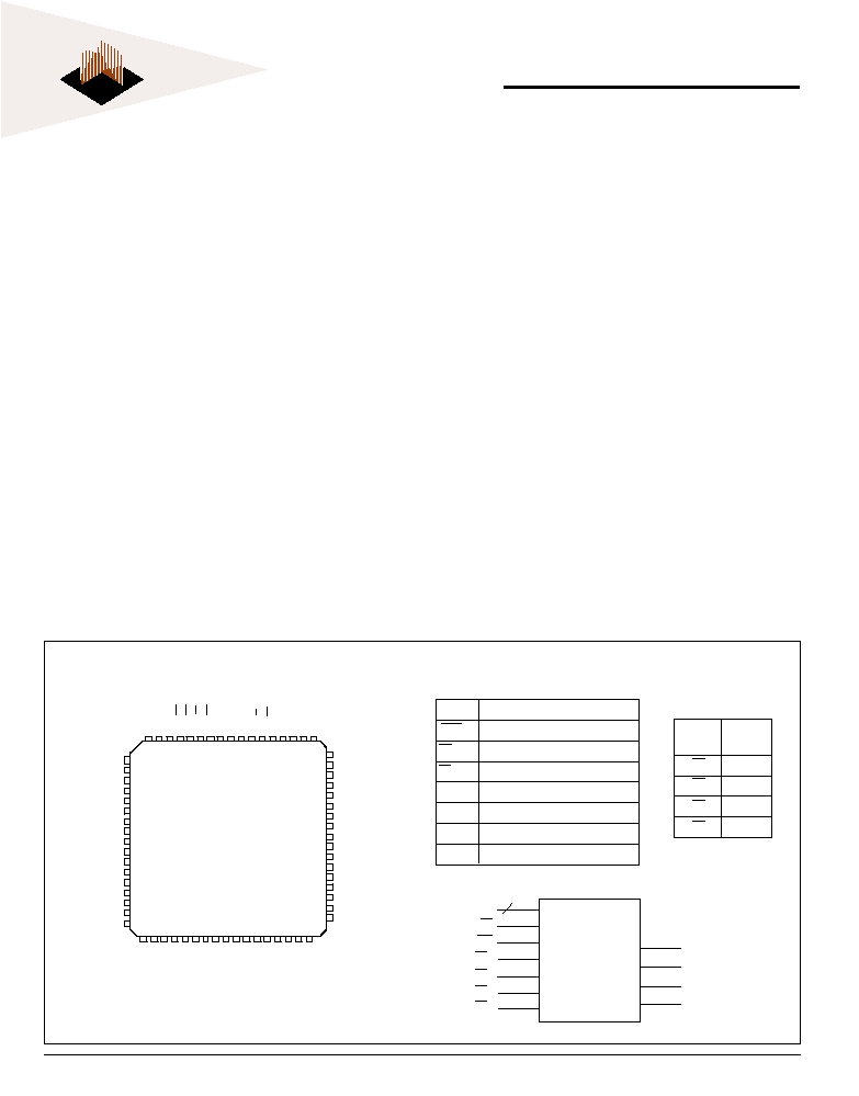
PIN NAMES
Chip
Byte
Enable Control
E
0
DQ
0-7
E
1
DQ
8-15
E
2
DQ
16-23
E
3
DQ
24-31
BYTE CONTROL
TABLE
A
0-18
Address Inputs
E
0-3
Chip Enables (One per Byte)
W
Master Write Enable
G
Master Output Enable
DQ
0-31
Common Data Input/Output
V
CC
Power (+5V �5%)
V
SS
Ground
NC
No Connection
PIN CONFIGURATIONS AND BLOCK DIAGRAM
FIG. 1
10
11
12
13
14
15
16
17
18
19
20
21
22
23
24
25
26
DQ17
DQ18
DQ19
V
SS
DQ20
DQ21
DQ22
DQ23
V
CC
DQ24
DQ25
DQ26
DQ27
V
SS
DQ28
DQ29
DQ30
60
59
58
57
56
55
54
53
52
51
50
49
48
47
46
45
44
DQ14
DQ13
DQ12
V
SS
DQ11
DQ10
DQ9
DQ8
V
CC
DQ7
DQ6
DQ5
DQ4
V
SS
DQ3
DQ2
DQ1
DQ31
27
28
29
30
31
32
33
34
35
36
37
38
39
40
41
42
43
A6
A5
A4
A3
A2
A1
A0
V
CC
A13
A12
A11
A10
A9
A8
A7
DQ0
9
DQ16
8
A18
7
A17
6E
3
5E
2
4E
1
3E
0
2N
C
1V
CC
68
N
C
67
N
C
66
G
65
W
6
4
A16
6
3
A15
6
2
A14
6
1
DQ15
A
0
-
18
G
W
E
0
E
1
E
2
E
3
DQ
0-7
DQ
8-15
DQ
16-23
DQ
24-31
512K x 32
Memory
Array
19
August 2000 Rev. 7
ECO #13097
2
White Electronic Designs Corporation Marlborough, MA (508) 485-4000
White Electronic Designs
EDI8L32512C
Parameter
Sym
Conditions
Min
Max
Units
12/15
17/20
m A
Operating Power Supply Current
I
CC1
W = V
IL
, I
I/O
= 0mA,
800
720
mA
Min Cycle
Standby (TTL) Supply Current
I
CC2
E � V
IH
, V
IN
� V
IL
or
200
200
mA
V
IN
� V
IH
, f = �MHz
Full Standby CMOS
I
CC3
E � V
CC
- 0.2V
40
40
mA
Supply Current
V
IN
� V
CC
- 0.2V or
V
IN
� 0.2V
Input Leakage Current
I
LI
V
IN
= 0V to VCC
�10
�A
Output Leakage Current
I
LO
V
I/O
= 0V to VCC
�10
�A
Output High Volltage
V
OH
I
OH
= -4.0mA
2.4
V
Output Low Voltage
V
OL
I
OL
= 8.0mA
0.4
V
ABSOLUTE MAXIMUM RATINGS*
RECOMMENDED DC OPERATING CONDITIONS
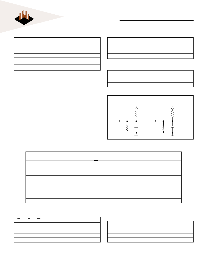
AC TEST CONDITIONS
(Note: For TEHQZ,TGHQZ and TWLQZ, CL = 5pF)
*Stress greater than those listed under "Absolute Maximum Ratings"
may cause permanent damage to the device. This is a stress rating
only and functional operation of the device at these or any other
conditions greater than those indicated in the operational sections of
this specification is not implied. Exposure to absolute maximum rating
conditions for extended periods may affect reliability.
DC ELECTRICAL CHARACTERISTICS
TRUTH TABLE
CAPACITANCE
(f=1.0MHz, V
IN
=V
CC
OR V
SS
)
FIG. 2
FIG. 3
30pF
480
Vcc
Q
255
5pF
480
Vcc
Q
255
Parameter
Sym
Min
Typ
Max
Units
Supply Voltage
V
CC
4.75
5.0
5.25
V
Supply Voltage
V
SS
0
0
0
V
Input High Voltage V
IH
2.2
--
V
CC
+0.5
V
Input Low Voltage V
IL
-0.3
--
0.8
V
Input Pulse Levels
V
SS
to 3.0V
Input Rise and Fall Times
5ns
Input and Output Timing Levels
1.5V
Output LoadFigure 2
Voltage on any pin relative to V
SS
-0.5V to 7.0V
Operating Temperature TA (Ambient)
Commercial
0�C to + 70�C
Industrial
-40�C to +85�C
Storage Temperature
-55�C to +125�C
Power Dissipation
5.0 Watts
Output Current.
20 mA
Junction Temperature, TJ
175�C
Parameter
Sym
Max
Unit
Address Lines
CI
30
pF
Data Lines
CD/Q
10
pF
Write & Output Enable Lines W, G
30
pF
Chip Enable Lines
E
0-3
8
pF
G
E
W
Mode
Output
Power
X
H
X
Standby
High Z
I
CC2
I
CC3
H
L
H
Output Deselect
High Z
I
CC1
L
L
H
ReadD
OUT
I
CC1
X
L
L
Write
D
IN
I
CC1

3
White Electronic Designs Corporation (508) 485-4000 www.whiteedc.com
White Electronic Designs
EDI8L32512C
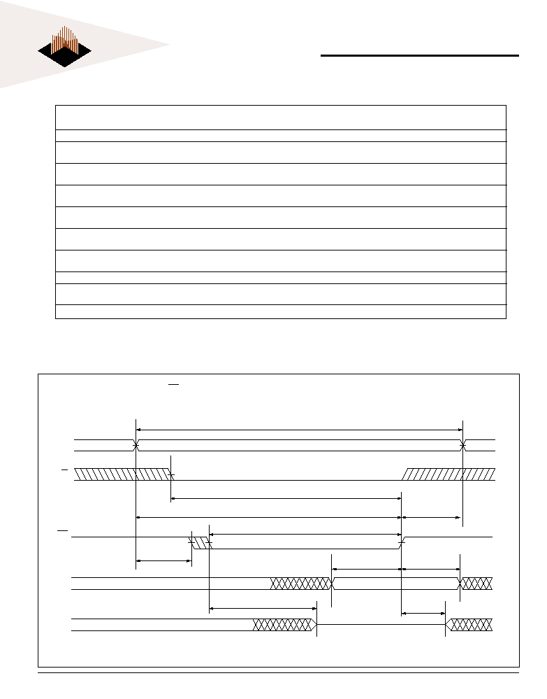
AC CHARACTERISTICS READ CYCLE
*Advanced Information
Note 1: Parameter guaranteed, but not tested.
FIG. 4
READ CYCLE 1 - W HIGH, G, E LOW
FIG. 5
READ CYCLE 2 - W HIGH
E
Q
TELQV
TGLQV
G
TAVQV
TELQX
TGLQX
TEHQZ
TGHQZ
A
TAVAV
TAVAV
ADDRESS 1
ADDRESS 2
TAVQX
TAVQV
DATA 1
DATA 2
Q
A
Symbol
12ns*
15ns
17ns
20ns
Parameter
JEDEC Alt. Min Max Min Max Min Max Min Max Units
Read Cycle Time
TAVAV
TRC 12
15
17
20 ns
Address Access Time
TAVQV
TAA
12
15
17 20 ns
Chip Enable Access Time
TELQV TACS
12
15
17
20 ns
Chip Enable to Output in Low Z (1) TELQX TCLZ 3
3 3
3 ns
Chip Disable to Output in High Z (1) TEHQZ TCHZ
6
7
9
9 ns
Output Hold from Address Change TAVQX
TOH 3
3 3
3
ns
Output Enable to Output Valid TGLQV
TOE
6
7
9
9 ns
Output Enable to Output in Low Z (1) TGLQX TOLZ 0
0
0
0 ns
Output Disable to Output in High Z(1) TGHQZ TOHZ
6
7
9
9 ns
4
White Electronic Designs Corporation Marlborough, MA (508) 485-4000
White Electronic Designs
EDI8L32512C
*Advanced Information.
Note 1: Parameter guaranteed, but not tested.
AC CHARACTERISTICS WRITE CYCLE
FIG. 6
WRITE CYCLE 1 - W CONTROLLED
TELWH
TWLWH
TWLQZ
DATA VALID
D
Q
TAVWH
TAVWL
TDVWH
HIGH Z
TWHDX
TWHAX
A
E
W
TAVAV
TWHQX
Symbol
12ns* 15ns
17ns
20ns
Parameter
JEDEC Alt. Min Max Min Max Min Max Min Max Units
Write Cycle Time
TAVAV TWC 12 15
17
20
ns
Chip Enable to End of Write
TELWH TCW 8 10
11
12
ns
TELEH TCW 8 10
11
12
ns
Address Setup Time
TAVWL TAS 0 0
0
0
ns
TAVEL TAS 0 0
0
0
ns
Address Valid to End of Write TAVWH TAW 8 10
11
12
ns
TAVEH TAW 8 10
11
12
ns
Write Pulse Width
TWLWH TWP 8 10
11
12
ns
TWLEH TWP 10 12
13
14
ns
Write Recovery Time
TWHAX TWR 0 0
0
0
ns
TEHAX TWR 0 0
0
0
ns
Data Hold Time
TWHDX TDH 0 0
0
0
ns
TEHDX TDH 0 0
0
0
ns
Write to Output in High Z (1)
TWLQZ TWHZ 0 6 0
7 0
8 0 9 ns
Data to Write Time
TDVWH TDW 6 7
8
9
ns
TDVEH TDW 6 7
8
9
ns
Output Active from End of Write (1) TWHQX TWLZ 3 3
3
3
ns
