
1
White Electronic Designs Corporation ∑ (602) 437-1520 ∑ www.wedc.com
White Electronic Designs
EDI8L32512V
October. 2000
Rev. 3
White Electronic Designs Corp. reserves the right to change products or specifications without notice.
FEATURES
DSP Memory Solution
ADSP-21060L (SHARC)
ADSP-21062L (SHARC)
Texas Instruments TMS320LC31
RISC Memory Solution
MPC860 (Power Quic)
Random Access Memory Array
Fast Access Times: 12, 15, 17, and 20ns
Individual Byte Enables
User configuration organization with Minimal
Additional Logic
Master Output Enable and Write Control
TTL Compatible Inputs and Outputs
Fully Static, No Clocks
Surface Mount Package
68 Lead PLCC, No. 99 JEDEC MO-47AE
Small Footprint, 0.990 Sq. In.
Multiple Ground Pins for Maximum Noise
Immunity
Single +3.3V (±5%) Supply Operation
DESCRIPTION
The EDI8L32512V is a high speed, 3.3V, 16 megabit SRAM.
The device is available with access times of 12, 15, 17 and
20ns allowing the creation of a no wait state DSP and RISC
microprocessor memory solutions.
The device can be configured as a 512K x 32 and used to
create a single chip external data memory solution for TI's
TMS320LC31 (figure 5), or Analog's SHARC
TM
DSP (figure
6).
The device provides a 56% space savings when compared
to four 512Kx8, 36 pin SOJs. In addition the EDI8K32512V
has only a 10pF load on the data lines vs. 32 pF for four
plastic SOJs.
The device provides a memory upgrade of the EDI8F32256V
(256K x 32) or the EDI8L32128V (128K x 32) (figure 8).
Alternatively, the device's chip enables can configure it as
a 1M x 16. A 1M x 48 program memory array for Analog's
CHARC DSP is created using three devices (figure 7).
If
this memory is too deep, two 512K x 24s (EDI8L24512V)
can be used to create a 512K x 48 array or two 128K x
24s (EDI8L24128V) can be used to create a 128K x 48
array.
Note: Soldier Reflow Temperature should not exceed 260∞C for 10 seconds.
512Kx32 SRAM Module.3.3V
PIN CONFIGURATIONS
PIN DESCRIPTION
FIG. 1
A0-A18
Address Inputs
E0#-E3#
Chip Enables
(One per Byte)
W#
Master Write Enable
G#
Master Output Enable
DQ0-DQ31
Common Data
Input/Output
V
CC
Power (+3.3V±5%)
V
SS
Ground
NC
No Connectiona
10
11
12
13
14
15
16
17
18
19
20
21
22
23
24
25
26
DQ17
DQ18
DQ19
V
SS
DQ20
DQ21
DQ22
DQ23
V
CC
DQ24
DQ25
DQ26
DQ27
V
SS
DQ28
DQ29
DQ30
60
59
58
57
56
55
54
53
52
51
50
49
48
47
46
45
44
DQ14
DQ13
DQ12
V
SS
DQ11
DQ10
DQ9
DQ8
V
CC
DQ7
DQ6
DQ5
DQ4
V
SS
DQ3
DQ2
DQ1
D
Q
3
1
2
7 28 29 30 31 32 33 34 35 36 37 38 39 40 41 42 43
A
6 A5 A4 A3 A2 A1 A0
V
C
C
A
1
3
A
1
2
A
1
1
A
1
0 A9 A8 A7
D
Q
0
9
D
Q
1
6
8
A
1
8
7
A
1
7
6
E
3
#
5
E
2
#
4
E
1
#
3
E
0
#
2
N
C
1
V
C
C
6
8
N
C
6
7
N
C
6
6
G
#
6
5
W
#
6
4
A
1
6
6
3
A
1
5
6
2
A
1
4
6
1
D
Q
1
5
BLOCK DIAGRAM
A0-18
G#
W#
E0#
E1#
E2#
E3#
DQ0-DQ7
DQ8-DQ15
DQ16-DQ23
DQ24-DQ31
512K x 32
Memory
Array
19

2
White Electronic Designs Corporation ∑ (602) 437-1520 ∑ www.wedc.com
White Electronic Designs
EDI8L32512V
October. 2000
Rev. 3
White Electronic Designs Corp. reserves the right to change products or specifications without notice.
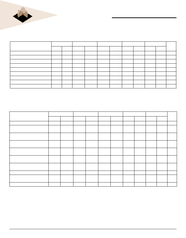
ABSOLUTE MAXIMUM RATINGS*
RECOMMENDED DC OPERATING
CONDITIONS
DC ELECTRICAL CHARACTERISTICS
CAPACITANCE
TRUTH TABLE
(f=1.0MHz, V
IN
=V
CC
or V
SS
)
*Stress greater than those listed under "Absolute Maximum Ratings" may cause
permanent damage to the device. This is a stress rating only and functional operation
of the device at these or any other conditions greater than those indicated in the
operational sections of this specification is not implied. Exposure to absolute maximum
rating conditions for extended periods may affect reliability.
(Note: For t
EHQZ
,t
GHQZ
and t
WLQZ
, CL = 5pF, Figure 2)
Voltage on any pin relative to V
SS
-0.5V to 7.0V
Operating Temperature t
A
(Ambient)
Commercial
0∞C to +70∞C
Industrial
-40∞C to +85∞C
Storage Temperature, Plastic
-55∞C to +125∞C
Power Dissipation
2.5 Watts
Output Current
20 mA
Junction Temperature, t
J
-175∞C
Parameter
Sym
Min
Typ
Max
Units
Supply Voltage
V
CC
3.135
3.3
3.465
V
Supply Voltage
V
SS
0
0
0
V
Input High Voltage
V
IH
2.2
--
V
CC
+ 0.3
V
Input Low Voltage
V
IL
-0.3
--
+0.8
V
AC TEST CONDITIONS
Input Pulse Levels
V
SS
to 3.0V
Input Rise and Fall Times
5ns
Input and Output Timing Levels
1.5V
Output Load
Figure 1
Parameter
Sym
Conditions
12 & 15
17 & 20
Units
Min
Typ
Max
Min
Typ
Max
Operating Power Supply Current
I
CC
1
W# = V
IL
, II/O = 0mA, Min Cycle
--
440
800
--
440
640
mA
Standby (TTL) Power Supply Current
I
CC
2
E# > V
IH
, V
IN
< V
IL
or V
IN
> V
IH
--
100
300
--
100
200
mA
Full Standby Power CMOS Supply
Current
I
CC
3
E# > V
CC
-0.2V
V
IN
> V
CC
=0.2V or V
IN
< 0.2V
--
60
80
--
60
100
mA
Input Leakage Current
I
LI
V
IN
= 0V to V
CC
--
--
±20
--
--
±10
µA
Output Leakage Current
I
LO
V I/O = 0V TO V
CC
--
--
±20
--
--
±10
µA
Output High Voltage
V
OH
I
OH
= -4.0mA
2.4
--
--
2.4
--
--
V
Output Low Voltage
V
OL
I
OL
= 4.0mA
--
--
0.4
--
--
0.4
V
E#
W#
G#
Mode
Output
Power
H
X
X
Standby
HIGH Z
I
CC
2, I
CC
3
L
H
H
Output
Deselect
HIGH Z
I
CC
1
L
H
L
Read
D
OUT
I
CC
1
L
L
X
Write
D
IN
I
CC
1
Parameter
Sym
Max
Unit
Address Lines
CI
30
pF
Data Lines
CD/Q
10
pF
Chip Enable Line
E0-3
8
pF
Write & Output Enable Line
W#, G#
30
pF
(V
CC
= 3.3V, t
A
= 25∞C)
30pF
480
Vcc
Q
Figure 1
Figure 2
255
5pF
480
Vcc
Q
255
3
White Electronic Designs Corporation ∑ (602) 437-1520 ∑ www.wedc.com
White Electronic Designs
EDI8L32512V
October. 2000
Rev. 3
White Electronic Designs Corp. reserves the right to change products or specifications without notice.
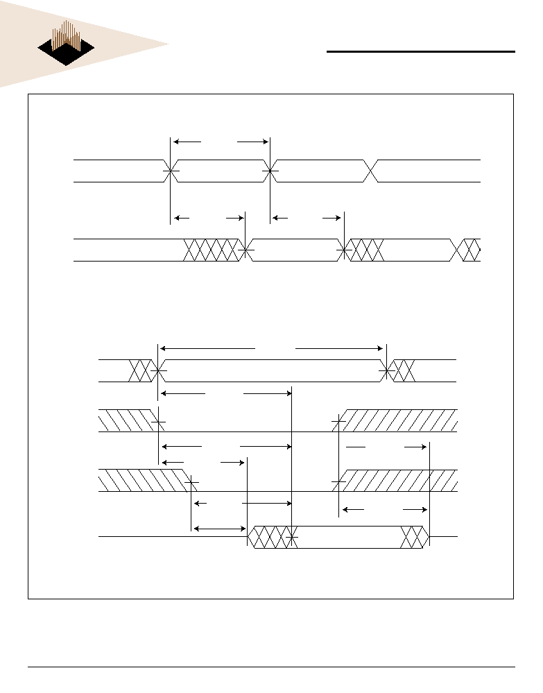
AC CHARACTERISTICS READ CYCLE
Notes: 1. Parameter is guaranteed by design but not tested.
Parameter
Symbol
12ns
15ns
17ns
20ns
Units
JEDEC
Alt.
Min
Max
Min
Max
Min
Max
Min
Max
Read Cycle Time
t
AVAV
t
RC
12
15
17
20
ns
Address Access Time
t
AVQV
t
AA
12
15
17
20
ns
Chip Enable Access
t
ELQV
t
ACS
10
12
15
20
ns
Chip Enable to Output in Low Z (1)
t
ELQX
t
CLZ
3
3
3
3
ns
Chip Disable to Output in High Z (1)
t
EHQZ
t
CHZ
6
7
8
9
ns
Output Hold from Address Change
t
AVQX
t
OH
3
3
3
3
ns
Output Enable to Output Valid
t
GLQV
t
OE
6
7
8
9
ns
Output Enable to Output in Low Z (1)
t
GLQX
t
OLZ
3
3
3
3
ns
Output Disable to Output in High (1)
t
GHQZ
t
OHZ
6
7
8
9
ns
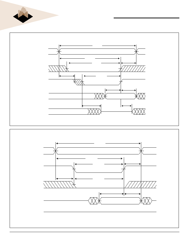
AC CHARACTERISTICS WRITE CYCLE
Notes: 1. Parameter guaranteed, but not tested.
Parameter
Symbol
12ns
15ns
17ns
20ns
Units
JEDEC
Alt.
Min
Max
Min
Max
Min
Max
Min
Max
Write Cycle Time
t
AVAV
t
WC
12
15
17
20
ns
Chip Enable to End of Write
t
ELWH
t
ELEH
t
CW
t
CW
8
8
10
10
11
11
12
12
ns
ns
Address Setup Time
t
AVWL
t
AVEL
t
AS
t
AS
0
0
0
0
0
0
0
0
ns
ns
Address Valid to End of Write
t
AVWH
t
AHEH
t
AW
t
AW
8
8
10
10
11
11
12
12
ns
ns
Write Pulse Width
t
WLWH
t
ELEH
t
WP
t
WP
8
8
10
10
11
11
12
12
ns
ns
Write Recovery Time
t
WHAX
t
EHAX
t
WR
t
WR
0
0
0
0
0
0
0
0
ns
ns
Data Hold Time
t
WHDX
t
EHDX
t
DH
t
DH
0
0
0
0
0
0
0
0
ns
ns
Write to Output in High Z (1)
t
WLQZ
t
WHZ
0
6
0
7
0
8
0
9
ns
Data to Write Time
t
DVWH
t
DVEH
t
DW
t
DW
6
6
7
7
8
8
9
9
ns
ns
Output Active from End of Write (1)
t
WHQX
t
WLZ
3
3
3
3
ns
(V
CC
= 3.3V, V
SS
= 0V, t
A
= 0∞C to -70∞C)
(V
CC
= 3.3V, V
SS
= 0V, t
A
= 0∞C to -70∞C)
4
White Electronic Designs Corporation ∑ (602) 437-1520 ∑ www.wedc.com
White Electronic Designs
EDI8L32512V
October. 2000
Rev. 3
White Electronic Designs Corp. reserves the right to change products or specifications without notice.
FIG. 2
TIMING WAVEFRONT - READ CYCLE
A
Q
READ CYCLE 1 (W# HIGH; G#, E# LOW)
t
AVQX
t
AVQV
t
AVAV
DATA 2
ADDRESS 1
ADDRESS 2
DATA 1
A
Q
READ CYCLE 2 (W# HIGH)
t
AVQV
t
ELQV
t
GLQV
t
ELQX
t
GLQX
t
AVAV
t
EHQZ
t
GHQZ
G#
E#
5
White Electronic Designs Corporation ∑ (602) 437-1520 ∑ www.wedc.com
White Electronic Designs
EDI8L32512V
October. 2000
Rev. 3
White Electronic Designs Corp. reserves the right to change products or specifications without notice.
FIG. 3
WRITE CYCLE - W# CONTROLLED
FIG. 4
WRITE CYCLE - E# CONTROLLED
A
D
WRITE CYCLE 1, W# CONTROLLED
t
AVWH
t
ELWH
t
WHAX
t
WLWH
t
DVWH
t
WLQZ
t
WHQX
t
AVWL
t
WHDX
t
AVAV
DATA VALID
HIGH Z
W#
E#
Q
A
D
WRITE CYCLE 2, E# CONTROLLED
t
AVEH
t
ELEH
t
EHAX
t
DVEH
t
EHDX
t
AVAV
DATA VALID
HIGH Z
W#
t
WLEH
E#
Q
t
AVEL

6
White Electronic Designs Corporation ∑ (602) 437-1520 ∑ www.wedc.com
White Electronic Designs
EDI8L32512V
October. 2000
Rev. 3
White Electronic Designs Corp. reserves the right to change products or specifications without notice.
ORDERING INFORMATION
Commercial Temperature Range (0∞C to +70∞C)
Part Number
Speed
(ns)
Package
No.
EDI8L32512V12AC
12
99
EDI8L32512V15AC
15
99
EDI8L32512V17AC
17
99
EDI8L32512V20AC
20
99
Industrial Temperature Range (-40∞C to +85∞C)
Part Number
Speed
(ns)
Package
No.
EDI8L32512V15AI
15
99
EDI8L32512V17AI
17
99
EDI8L32512V20AI
20
99
ALL DIMENSIONS ARE IN INCHES
0.956
Max
0.180
Max
0.115
Max
0.040
Max
0.050
BSC
0.020
0.015
0.995
Max
0.930
0.890
0.956
Max
0.995
Max
PACKAGE 99" 68 LEAD PLCC
JEDEC MO-47AE
Coplanarity (lowest lead to
highest lead 0.004 max)
7
White Electronic Designs Corporation ∑ (602) 437-1520 ∑ www.wedc.com
White Electronic Designs
EDI8L32512V
October. 2000
Rev. 3
White Electronic Designs Corp. reserves the right to change products or specifications without notice.
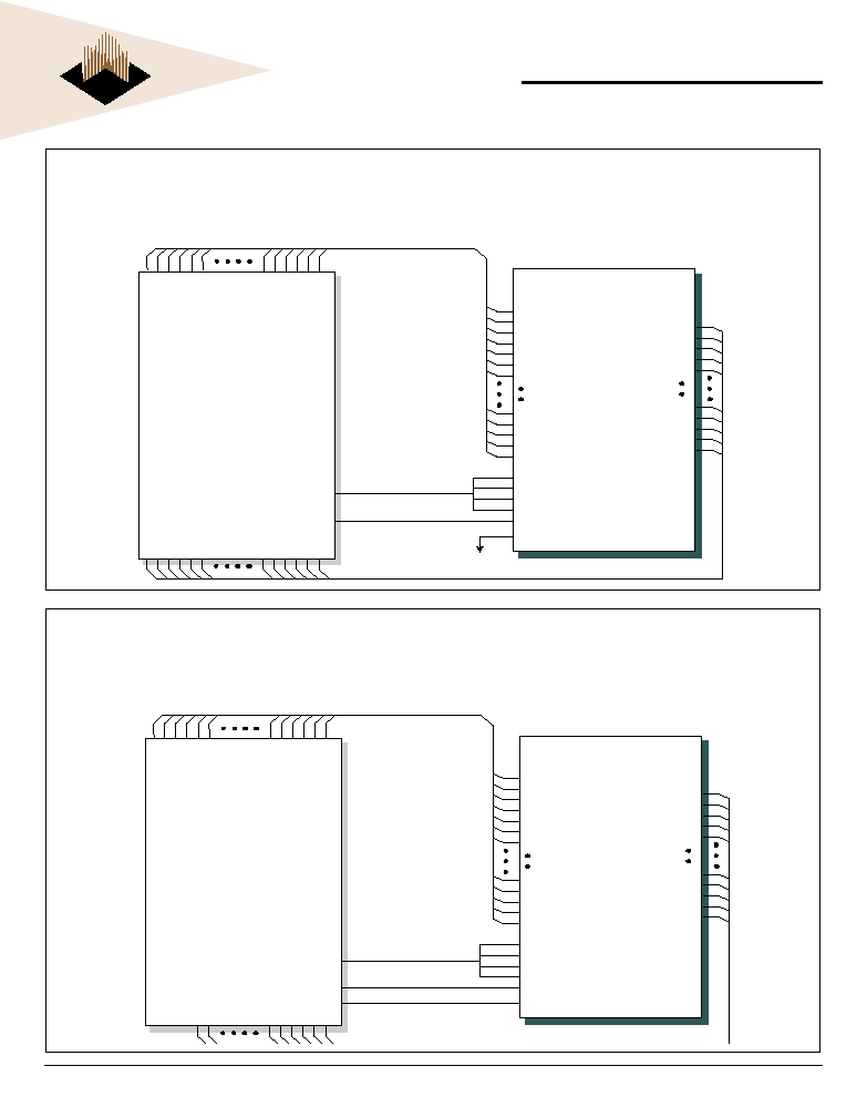
FIG 5.
INTERFACING THE TEXAS INSTRUMENTS TMS 320LC32 WITH THE
EDI8L32512V (512K X 32)
FIG 6.
INTERFACING THE ANALOG SHARC DSP WITH THE EDI8L32512V
(512K X 32 ARRAY).
Primary Address Bus
A
23
-
0
EDI8L32512V
E0#
E1#
E2#
E3#
W#
G#
STRB#
R/W#
Primary Databus
D31 - D0
A18
A17
A16
A15
A14
A13
A12
A4
A3
A2
A1
A0
DQ31
DQ30
DQ29
DQ28
DQ27
DQ4
DQ3
DQ2
DQ1
DQ0
A
D
D
R
E
S
S
B
U
S
D
A
T
A
B
U
S
}
8L32512C only
TI TMS320LC31
Address Bus
A
31
-
0
EDI8L32512V
E0#
E1#
E2#
E3#
W#
G#
MS0#
WR#
RD#
Databus
A18
A17
A16
A15
A14
A13
A12
A4
A3
A2
A1
A0
DQ31
DQ30
DQ29
DQ28
DQ27
DQ4
DQ3
DQ2
DQ1
DQ0
A
D
D
R
E
S
S
B
U
S
D
A
T
A
B
U
S
Analog Device
ADSP-2106xL
D31-0
D31 D30 . . . .
D5 D4 D3 D2 D1 D0
8
White Electronic Designs Corporation ∑ (602) 437-1520 ∑ www.wedc.com
White Electronic Designs
EDI8L32512V
October. 2000
Rev. 3
White Electronic Designs Corp. reserves the right to change products or specifications without notice.
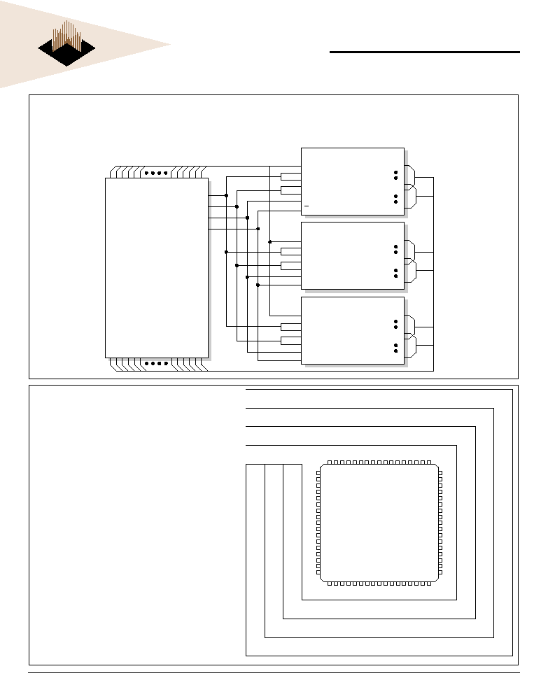
FIG 7.
INTERFACING THE ANALOG SHARC DSP WITH
THE EDI8L32512V (1M X 48 ARRAY)
FIG 8.
MCM-L UPGRADE PATH
DQ
31
DQ
16
DQ
15
DQ
0
D
A
T
A
B
U
S
A18-0
E0#
E1#
E2#
E3#
W#
G#
DQ
15
WORD1
DQ
0
DQ
31
DQ
16
DQ
15
DQ
0
D
A
T
A
B
U
S
DQ
31
WORD2
DQ
16
DQ
31
DQ
16
DQ
15
DQ
0
D
A
T
A
B
U
S
DQ
47
WORD3
DQ
17
EDI8L32512V
(Configured as 1Mx16)
EDI8L32512V
(Configured as 1Mx16)
EDI8L32512V
(Configured as 1Mx16)
Address Bus
A
31
-
0
Analog Device
ADSP-2106xL
MS0#
MS1#
WR#
Databus
D
47
-
0
RD#
A18-0
E0#
E1#
E2#
E3#
W#
G#
A18-0
E0#
E1#
E2#
E3#
W#
G#
512Kx32
256Kx32
128Kx32
E
3
#
E
2
#
E
0
#
G
#
W
#
10
11
12
13
14
15
16
17
18
19
20
21
22
23
24
25
26
60
59
58
57
56
55
54
53
52
51
50
49
48
47
46
45
44
2
7 28 29 30 31 32 33 34 35 36 37 38 39 40 41 42 43
9 8 7 6 5 4 3 2 1 68 67 66 65 64 63 62 61
D
Q
3
1
A
6 A5 A4 A3 A2 A1 A0 V
C
C
A
1
3
A
1
2
A
1
1
A
1
0
A
0
9
A
0
8
A
0
7
D
Q
0
0
D
Q
3
1
A
6 A5 A4 A3 A2 A1 A0 V
C
C
A
1
3
A
1
2
A
1
1
A
1
0
A
0
9
A
0
8
A
0
7
D
Q
0
0
D
Q
3
1
A
6 A5 A4 A3 A2 A1 A0 V
C
C
A
1
3
A
1
2
A
1
1
A
1
0
A
0
9
A
0
8
A
0
7
D
Q
0
0
D
Q
1
6
N
C
N
C
E
3
#
E
2
#
E
1
#
E
0
#
N
C
V
C
C
N
C
N
C
G
#
W
#
A
1
6
A
1
5
A
1
4
D
Q
1
5
D
Q
1
6
N
C
A
1
7
B
5
3
#
B
5
2
#
B
5
1
#
B
5
0
#
E
1
#
V
C
C
N
C
E
0
#
G
#
W
#
A
1
6
A
1
5
A
1
4
D
Q
1
5
D
Q
1
6
A
1
8
A
1
7
E
1
#
N
C
V
C
C
N
C
N
C
A
1
6
A
1
5
A
1
4
D
Q
1
5
DQ17
DQ18
DQ19
V
SS
DQ20
DQ21
DQ22
DQ23
V
CC
DQ24
DQ25
DQ26
DQ27
V
SS
DQ28
DQ29
DQ30
DQ14
DQ13
DQ12
V
SS
DQ11
DQ10
DQ09
DQ08
V
CC
DQ07
DQ06
DQ05
DQ04
V
SS
DQ03
DQ02
DQ01
DQ14
DQ13
DQ12
V
SS
DQ11
DQ10
DQ09
DQ08
V
CC
DQ07
DQ06
DQ05
DQ04
V
SS
DQ03
DQ02
DQ01
DQ14
DQ13
DQ12
V
SS
DQ11
DQ10
DQ09
DQ08
V
CC
DQ07
DQ06
DQ05
DQ04
V
SS
DQ03
DQ02
DQ01
8L32512V
8L32256V
8L32128V
DQ17
DQ18
DQ19
V
SS
DQ20
DQ21
DQ22
DQ23
V
CC
DQ24
DQ25
DQ26
DQ27
V
SS
DQ28
DQ29
DQ30
DQ17
DQ18
DQ19
V
SS
DQ20
DQ21
DQ22
DQ23
V
CC
DQ24
DQ25
DQ26
DQ27
V
SS
DQ28
DQ29
DQ30