1
White Electronic Designs Corporation ∑ (508) 366-5151 ∑ www.whiteedc.com
EDI8L32512V
512Kx32 SRAM MODULE, 3.3V
FEATURES
s DSP Memory Solution
∑ ADSP-21060L (SHARC)
∑ ADSP-21062L (SHARC)
∑Texas Instruments TMS320LC31
s RISC Memory Solution
∑ MPC860 (Power Quic)
s Random Access Memory Array
∑ Fast Access Times: 12, 15, 17, and 20ns
∑ Individual Byte Enables
∑ User configurable organization with Minimal Additional Logic
∑ Master Output Enable and Write Control
∑ TTL Compatible Inputs and Outputs
∑ Fully Static, No Clocks
s Surface Mount Package
∑ 68 Lead PLCC, No. 99 JEDEC M0-47AE
∑ Small Footprint, 0.990 Sq. In.
∑ Multiple Ground Pins for Maximum Noise Immunity
s Single +3.3V (
±
5%) Supply Operation
October 2000 Rev. 3
ECO# 13316
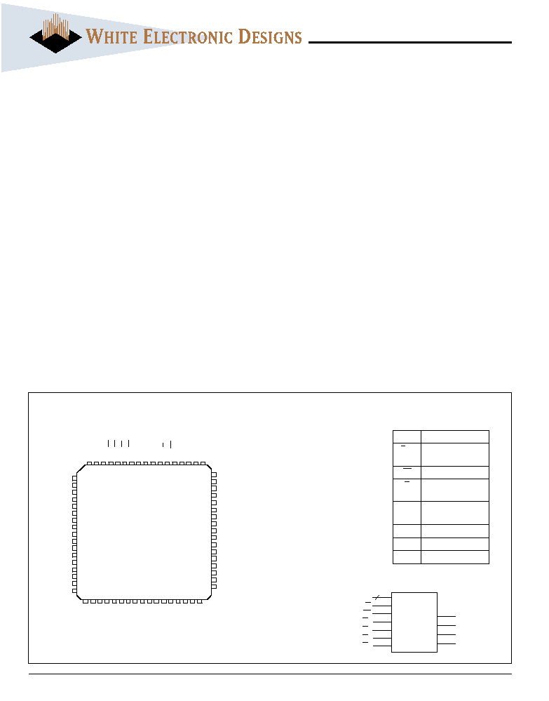
PIN DESCRIPTION
A
0-18
Address Inputs
E
0-3
Chip Enables
(One per Byte)
W
Master Write Enable
G
Master Output
Enable
DQ
0-31
Common Data
Input/Output
V
CC
Power (+3.3V
±
5%)
V
SS
Ground
NC
No Connection
BLOCK DIAGRAM
FIG. 1
PIN CONFIGURATION
The EDI8L32512V is a high speed, 3.3V, 16 megabit SRAM. The
device is available with access times of 12, 15, 17 and 20ns
allowing the creation of a no wait state DSP and RISC micropro-
cessor memory solutions.
The device can be configured as a 512K x 32 and used to create a
single chip external data memory solution for TI's TMS320LC31
(figure 5), or Analog's SHARCTM DSP (figure 6).
The device provides a 56% space savings when compared to four
512K x 8, 36 pin SOJs. In addition the EDI8L32512C has only a 10pF
load on the data lines vs. 32pf for four plastic SOJs.
The device provides a memory upgrade of the EDI8L32256V (256K
x 32) or the EDI8L32128V (128K x 32) (figure 8). Alternatively, the
device's chip enables can configure it as a 1M x 16. A 1Mx 48
program memory array for Analog's SHARC DSP is created using
three devices (figure 7). If this memory is too deep, two 512K x 24s
(EDI8L24512V) can be used to create a 512K x 48 array or two 128K
x 24s (EDI8L24128V) can be used to create a 128K x 48 array.
Note:
Solder Reflow Temperature should not exceed 260
∞
C for 10 seconds.
TOP VIEW
NOTE:
For memory upgrade information, refer to Page 7, Figure 8 "EDI
MCM-L upgrade path.
10
11
12
13
14
15
16
17
18
19
20
21
22
23
24
25
26
DQ17
DQ18
DQ19
V
SS
DQ20
DQ21
DQ22
DQ23
V
CC
DQ24
DQ25
DQ26
DQ27
V
SS
DQ28
DQ29
DQ30
60
59
58
57
56
55
54
53
52
51
50
49
48
47
46
45
44
DQ14
DQ13
DQ12
V
SS
DQ11
DQ10
DQ9
DQ8
V
CC
DQ7
DQ6
DQ5
DQ4
V
SS
DQ3
DQ2
DQ1
DQ31
27
28
29
30
31
32
33
34
35
36
37
38
39
40
41
42
43
A6
A5
A4
A3
A2
A1
A0
V
CC
A13
A12
A11
A10
A9
A8
A7
DQ0
9D
Q
1
6
8
A18
7
A17
6E
3
5E
2
4E
1
3E
0
2N
C
1V
CC
68
N
C
67
N
C
66
G
65
W
6
4
A16
6
3
A15
6
2
A14
6
1
DQ15
A
0
-
18
G
W
E
0
E
1
E
2
E
3
DQ
0
-DQ
7
DQ
8
-DQ
15
DQ
16
-DQ
23
DQ
24
-DQ
31
512K x 32
Memory
Array
19
2
White Electronic Designs Corporation ∑ (508) 366-5151 ∑ www.whiteedc.com
EDI8L32512V
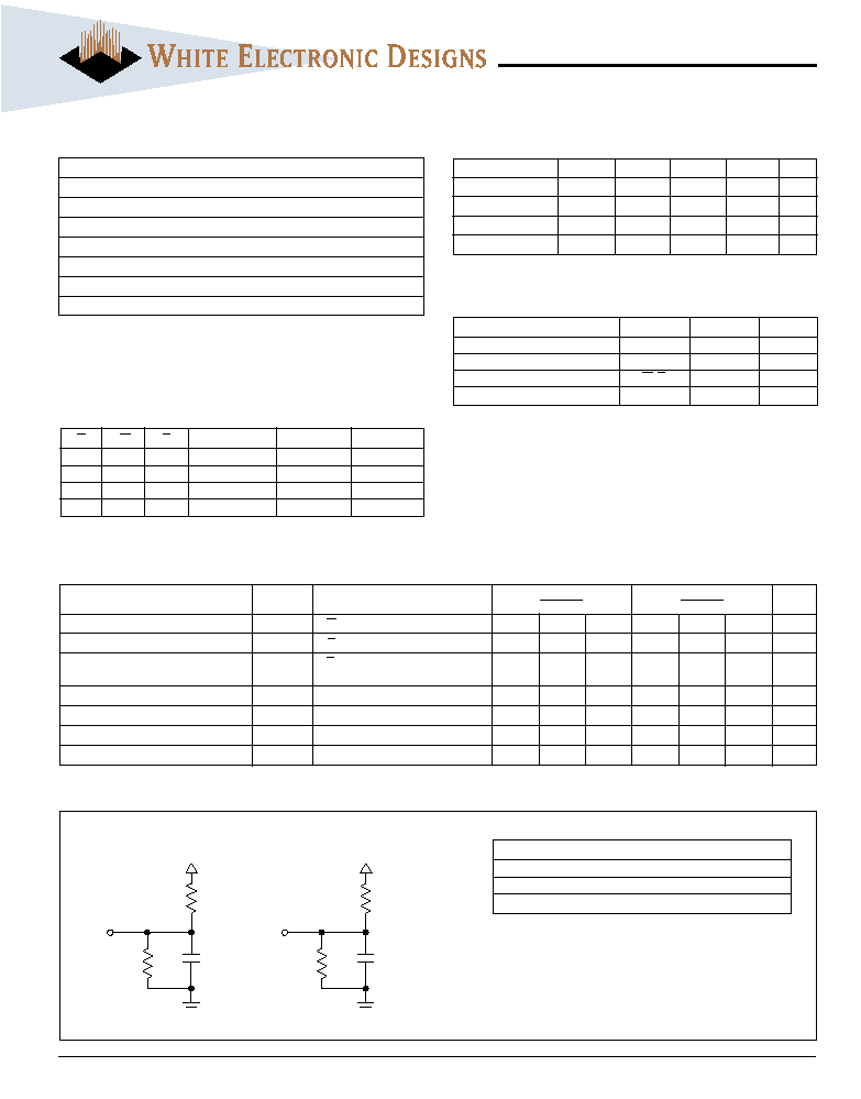
ABSOLUTE MAXIMUM RATINGS
Voltage on any pin relative to V
SS
-0.5V to 7.0V
Operating Temperature T
A
(Ambient)
Commercial
0
∞
C to +70
∞
C
Industrial
-40
∞
C to +85
∞
C
Storage Temperature, Plastic
-55
∞
C to +125
∞
C
Power Dissipation
2.5 Watts
Output Current
20 mA
Junction Temperature, T
J
+175
∞
C
RECOMMENDED OPERATING CONDITIONS
Parameter
Symbol
Min
Typ
Max
Unit
Supply Voltage
V
CC
3.135
3.3
3.465
V
Supply Voltage
V
SS
0
0
0
V
Input High Voltage
V
IH
2.2
--
Vcc +0.3
V
Input Low Voltage
V
IL
-0.3
--
+0.8
V
TRUTH TABLE
E
W
G
Mode
Output
Power
H
X
X
Standby
High Z
Icc
2
, Icc
3
L
H
H
Output Deselect
High Z
Icc
1
L
H
L
Read
Data Out
Icc
1
L
L
X
Write
Data In
Icc
1
* Stress greater than those listed under "Absolute Maximum Ratings" may cause
permanent damage to the device. This is a stress rating only and functional
operation of the device at these or any other conditions greater than those indi-
cated in the operational sections of this specification is not implied. Exposure to
absolute maximum rating conditions for extended periods may affect reliability.
Parameter
Symbol
Conditions
12 & 15
17 & 20
Units
Min
Typ
Max
Min
Typ
Max
Operating Power Supply Current
I
CC1
W = V
IL
, I
I/O
= 0mA, Min Cycle
--
440
720
--
440
640
mA
Standby (TTL) Power Supply Current
I
CC2
E
V
IH
, V
IN
V
IL
or V
IN
V
IH
--
100
200
--
100
200
mA
Full Standby Power CMOS
I
CC3
E
V
CC
-0.2V
--
60
100
--
60
100
mA
Supply Current
V
IN
V
CC
-0.2V or V
IN
0.2V
Input Leakage Current
I
LI
V
IN
= 0V to V
CC
--
--
±
10
--
--
±
10
µ
A
Output Leakage Current
I
LO
V
I/O
= 0V to V
CC
--
--
±
10
--
--
±
10
µ
A
Output High Voltage
V
OH
I
OH
= -4.0mA
2.4
--
--
2.4
--
--
V
Output Low Voltage
V
OL
I
OL
= 4.0mA
--
--
0.4
--
--
0.4
V
DC ELECTRICAL CHARACTERISTICS
(V
CC
= 3.3V, T
A
= 25∞C)
CAPACITANCE
(f = 1.0MHz, V
IN
= V
CC
or V
SS
)
Parameter
Sym
Max
Unit
Address Lines
C
I
30
pF
Data Lines
C
D/Q
10
pF
Write & Output Enable Line
W, G
30
pF
Chip Enable Line
E
0-3
8
pF
Input Pulse Levels
V
SS
to 3.0V
Input Rise and Fall Times
5ns
Input and Output Timing Levels
1.5V
Output Load
Figure 1
(NOTE: For t
EHQZ
, t
GHQZ
and t
WLQZ
, CL = 5pF, Figure 2)
30pF
480
Vcc
Q
Figure 1
Figure 2
255
5pF
480
Vcc
Q
255
AC TEST CONDITIONS
3
White Electronic Designs Corporation ∑ (508) 366-5151 ∑ www.whiteedc.com
EDI8L32512V
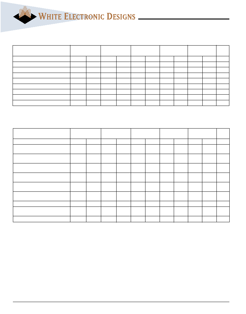
AC CHARACTERISTICS ≠ READ CYCLE
(V
CC
= 3.3V, V
ss
= 0V, T
A
= 0∞C to + 70∞C )
Symbol
12ns
15ns
17ns
20ns
Parameter
JEDEC
Alt.
Min
Max
Min
Max
Min
Max
Min
Max
Units
Read Cycle Time
t
AVAV
t
RC
12
15
17
20
ns
Address Access Time
t
AVQV
t
AA
12
15
17
20
ns
Chip Enable Access Time
t
ELQV
t
ACS
10
12
15
20
ns
Chip Enable to Output in Low Z (1)
t
ELQX
t
CLZ
3
3
3
3
ns
Chip Disable to Output in High Z (1)
t
EHQZ
t
CHZ
6
7
8
9
ns
Output Hold from Address Change
t
AVQX
t
OH
3
3
3
3
ns
Output Enable to Output Valid
t
GLQV
t
OE
6
7
8
9
ns
Output Enable to Output in Low Z (1)
t
GLQX
t
OLZ
3
3
3
3
ns
Output Disable to Output in High Z (1)
t
GHQZ
t
OHZ
6
7
8
9
ns
1. This parameter is guaranteed by design but not tested.
AC CHARACTERISTICS ≠ WRITE CYCLE
(V
CC
= 3.3V, V
ss
= 0V, T
A
= 0∞C to + 70∞C )
Symbol
12ns
15ns
17ns
20ns
Parameter
JEDEC
Alt.
Min
Max
Min
Max
Min
Max
Min
Max
Units
Write Cycle Time
t
AVAV
t
WC
12
15
17
20
ns
Chip Enable to End of Write
t
ELWH
t
CW
8
10
11
12
ns
t
ELEH
t
CW
8
10
11
12
ns
Address Setup Time
t
AVWL
t
AS
0
0
0
0
ns
t
AVEL
t
AS
0
0
0
0
ns
Address Valid to End of Write
t
AVWH
t
AW
8
10
11
12
ns
t
AVEH
t
AW
8
10
11
12
ns
Write Pulse Width
t
WLWH
t
WP
8
10
11
12
ns
t
ELEH
t
WP
8
10
11
12
ns
Write Recovery Time
t
WHAX
t
WR
0
0
0
0
ns
t
EHAX
t
WR
0
0
0
0
ns
Data Hold Time
t
WHDX
t
DH
0
0
0
0
ns
t
EHDX
t
DH
0
0
0
0
ns
Write to Output in High Z (1)
t
WLQZ
t
WHZ
0
6
0
7
0
8
0
9
ns
Data to Write Time
t
DVWH
t
DW
6
7
8
9
ns
t
DVEH
t
DW
6
7
8
9
ns
Output Active from End of Write (1)
t
WHQX
t
WLZ
3
3
3
3
ns
1. This parameter is guaranteed by design but not tested.

4
White Electronic Designs Corporation ∑ (508) 366-5151 ∑ www.whiteedc.com
EDI8L32512V
A
Q
READ CYCLE 1 (W HIGH; G, E LOW)
t
AVQX
t
AVQV
t
AVAV
DATA 2
ADDRESS 1
ADDRESS 2
DATA 1
A
Q
READ CYCLE 2 (W HIGH)
t
AVQV
t
ELQV
t
GLQV
t
ELQX
t
GLQX
t
AVAV
t
EHQZ
t
GHQZ
G
E
WS32K32-XHX
FIG. 2
TIMING WAVEFORM - READ CYCLE
FIG. 4
WRITE CYCLE - E CONTROLLED
FIG. 3
WRITE CYCLE - W CONTROLLED
A
D
WRITE CYCLE 2, E CONTROLLED
t
AVEH
t
ELEH
t
EHAX
t
DVEH
t
EHDX
t
AVAV
DATA VALID
HIGH Z
W
t
WLEH
E
Q
t
AVEL
A
D
WRITE CYCLE 1, W CONTROLLED
t
AVWH
t
ELWH
t
WHAX
t
WLWH
t
DVWH
t
WLQZ
t
WHQX
t
AVWL
t
WHDX
t
AVAV
DATA VALID
HIGH Z
W
E
Q
5
White Electronic Designs Corporation ∑ (508) 366-5151 ∑ www.whiteedc.com
EDI8L32512V
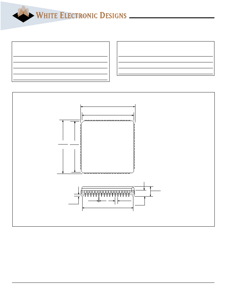
PACKAGE 99:
68 LEAD PLCC
JEDEC MO-47AE
ALL DIMENSIONS ARE IN INCHES
0.956
Max
0.180
Max
0.115
Max
0.040
Max
0.050
BSC
0.020
0.015
0.995
Max
0.930
0.890
0.956
Max
0.995
Max
Commercial Temperature Range (0
∞
C to +70
∞
C)
Part Number
Speed
Package
(ns)
No.
EDI8L32512V12AC
12
99
EDI8L32512V15AC
15
99
EDI8L32512V17AC
17
99
EDI8L32512V20AC
20
99
ORDERING INFORMATION
Industrial Temperature Range (-40
∞
C to +85
∞
C)
Part Number
Speed
Package
(ns)
No.
EDI8L32512V15AI
15
99
EDI8L32512V17AI
17
99
EDI8L32512V20AI
20
99
Coplanarity (lowest lead to
highest lead 0.004 max)