 | –≠–ª–µ–∫—Ç—Ä–æ–Ω–Ω—ã–π –∫–æ–º–ø–æ–Ω–µ–Ω—Ç: FEB01 | –°–∫–∞—á–∞—Ç—å:  PDF PDF  ZIP ZIP |

August 2000 Rev. 3 - ECO #13124
1
PCMCIA Flash Memory Card
FEB Series
PC Card Products
∑
Low cost Linear Flash Card
∑ Single 5 Volt Supply
∑Based on AMD Flash Components
- very low power without entering reset mode
- allows standard access from low power mode
∑Fast Read Performance
- 100ns or 150ns Maximum Access Time
∑ x8 Data Interface
∑ High Performance Random Writes
- 10µs Typical Word Write Time
∑ Automated Write and Erase Algorithms
- AMD Command Set
∑ 50µA Typical Deep Power-Down
∑ 100,000 Erase Cycles per Block
∑ 64K word symmetrical Block Architecture
∑ PC Card Standard Type I Form Factor
The FEB Econo Flash card series offers a low cost eight
bit linear Flash solid state storage solution for code/data
storage and embedded applications.
Packaged in PCMCIA type I or a type I half-card housing,
the FEB card series is based on AMD Flash memories:
Am29F080 (8Mb) or Am29F016 (16Mb) devices whose
device codes are D5h and ADh respectively. Systems
should be able to recognize both codes. The
symmetrically blocked architecture and 5V operation
provides a cost effective, high performance, nonvolatile
storage solution. The PC Card form factor offers an
industry standard pinout and mechanical outline, allowing
density upgrades without system design changes.
The FEB card series is designed as a simple x8 linear
array of Flash devices. The 2MB and 4MB density options
may be built with either 8Mb or 16Mb components. Both
components have uniform 64Kbyte sectors and use
identical embedded automated write and erase algorithms.
The 8 bit design provides very low power operation as
only one component is active at a time. The AMD based
components allow for very low standby currents without
entering Reset mode. This allows for standard access time
immediately from low power standby mode.
Eight Bit Flash Memory Card (AMD based) 1, 2, and 4 MEGABYTE
SUPPORTED COMPONENTS (max 4 X):
Am29F080 - max 4MB
CONTROL
LOGIC
DEVICE 0
DEVICE 1
DEVICE 2
DEVICE 3
ADDRESS BUS A0-A22
Am29F016 - max 8MB
A0-20(19)
CS0
CS1
CS2
CS3
CS0
CS1
CS2
CS3
CE1#
BVD1
BVD2
VPP1
VPP2
VS1
VS2
open
open
NC
NC
D0-D7
Vcc
CD1#
CD2#
GND
WE#
OE#
Vcc
WAIT#
Block Diagram
Features
General Description
August 2000 Rev. 3 - ECO #13124
2
PCMCIA Flash Memory Card
FEB Series
PC Card Products
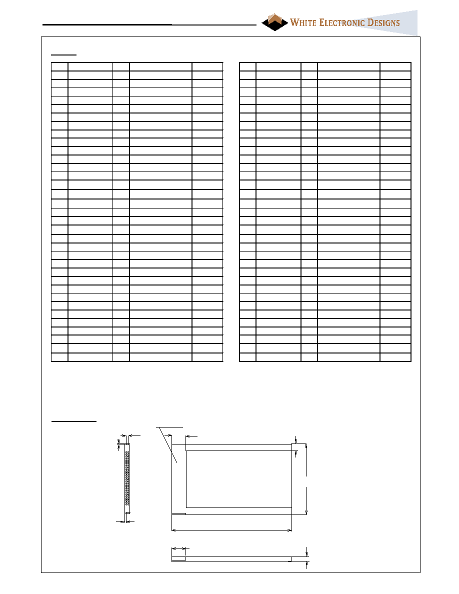
Pin Signal name
I/O
Function
Active
Pin Signal name
I/O
Function
Active
1
GND
Ground
35
GND
Ground
2
DQ3
I/O
Data bit 3
36
CD1#
O
Card Detect 1
LOW
3
DQ4
I/O
Data bit 4
37
DQ11
I/O
Data bit 11
N.C.
4
DQ5
I/O
Data bit 5
38
DQ12
I/O
Data bit 12
N.C.
5
DQ6
I/O
Data bit 6
39
DQ13
I/O
Data bit 13
N.C.
6
DQ7
I/O
Data bit 7
40
DQ14
I/O
Data bit 14
N.C.
7
CE1#
I
Card enable 1
LOW
41
DQ15
I
Data bit 15
N.C.
8
A10
I
Address bit 10
42
CE2#
I
Card Enable 2
N.C.
9
OE#
I
Output enable
LOW
43
VS1
O
Voltage Sense 1
N.C.
10
A11
I
Address bit 11
44
RFU
Reserved
11
A9
I
Address bit 9
45
RFU
Reserved
12
A8
I
Address bit 8
46
A17
I
Address bit 17
13
A13
I
Address bit 13
47
A18
I
Address bit 18
14
A14
I
Address bit 14
48
A19
I
Address bit 19
1MB
2)
15
WE#
I
Write Enable
LOW
49
A20
I
Address bit 20
2MB
2)
16
RDY/BSY#
O
Ready/Busy
N.C.
50
A21
I
Address bit 21
4MB
2)
17
Vcc
Supply Voltage
51
Vcc
Supply Voltage
18
Vpp1
12VProg. Voltage
N.C.
52
Vpp2
12V Prog. Voltage
N.C.
19
A16
I
Address bit 16
53
A22
I
Address bit 22
8MB
2)
20
A15
I
Address bit 15
54
A23
I
Address bit 23
N.C.
21
A12
I
Address bit 12
55
A24
I
Address bit 24
N.C.
22
A7
I
Address bit 7
56
A25
I
Address bit 25
N.C.
23
A6
I
Address bit 6
57
VS2
O
Voltage Sense 2
N.C.
24
A5
I
Address bit 5
58
RST
I
Card Reset
N.C.
25
A4
I
Address bit 4
59
Wait#
O
Extended Bus cycle
N.C.
26
A3
I
Address bit 3
60
RFU
Reserved
27
A2
I
Address bit 2
61
REG#
I
Attrib Mem Select
N.C.
28
A1
I
Address bit 1
62
BVD2
O
Bat. Volt. Detect 2
29
A0
I
Address bit 0
63
BVD1
O
Bat. Volt. Detect 1
30
DQ0
I/O
Data bit 0
64
DQ8
I/O
Data bit 8
N.C.
31
DQ1
I/O
Data bit 1
65
DQ9
I/O
Data bit 9
N.C.
32
DQ2
I/O
Data bit 2
66
DQ10
O
Data bit 10
N.C.
33
WP
O
Write Potect
1)
67
CD2#
O
Card Detect 2
LOW
34
GND
Ground
68
GND
Ground
Mechanical
54.0mm
±
0.10
(2.126")
10.0mm MIN
(0.400")
1.6mm
±
0.05
(0.063")
1.0mm
±
0.05
(0.039")
1.0mm
±
0.05
(0.039")
3.3mm
±
T1 (0.130")
T1=0.10mm interconnect area
T1=0.20mm substrate area
Interconnect area
10.0mm MIN
(0.400")
3.0mm MIN
85.6mm
±
0.20
(3.370")
Substrate area
Pinout
Notes:
1. Connected to GND - no write protection.
2. Shows density for which specified address bit is MSB. Higher order addresses are not connected (i.e. for 4MB card
A21 is MSB, A22-A25 are N.C.).

August 2000 Rev. 3 - ECO #13124
3
PCMCIA Flash Memory Card
FEB Series
PC Card Products
Symbol
Type
Name and Function
A0 - A25
INPUT
ADDRESS INPUTS: A0 through A25 enable direct addressing of
up to 64MB of memory on the card. The memory will wrap at the
card density boundary. The system should not try to access memory
beyond the card density. The upper addresses are not connected.
DQ0 ≠ DQ15
INPUT/OUT
DATA INPUT/OUTPUT: DQ0 THROUGH DQ15 constitute the
bi-directional databus. DQ0 - DQ7 constitute the lower (even) byte.
DQ8 ≠ DQ15 are not connected. DQ7 is the MSB.
CE1#, CE2#
INPUT
CARD ENABLE 1 AND 2: CE1# enables even byte accesses,
CE2# enables odd byte accesses. CE2# is not connected.
OE#
INPUT
OUTPUT ENABLE: Active low signal enabling read data from the
memory card.
WE#
INPUT
WRITE ENABLE: Active low signal gating write data to the
memory card.
RDY/BSY#
N.C.
READY/BUSY OUTPUT: Indicates status of internally timed erase
or program algorithms. A high output indicates that the card is ready
to accept accesses. This signal is not connected.
CD1#, CD2#
OUTPUT
CARD DETECT 1 and 2: Provide card insertion detection. These
signals are connected to ground internally on the memory card. The
host socket interface circuitry shall supply 10K-ohm or larger pull-up
resistors on these signal pins.
WP
OUTPUT
WRITE PROTECT: This signal is pulled low internally. This
signifies write protect = "off " for all cases.
VPP1, VPP2
N.C.
PROGRAM/ERASE POWER SUPPLY: 12V. Not connected for
5V only card.
VCC
CARD POWER SUPPLY: 5.0V
GND
GROUND: for all internal circuitry.
REG#
N.C.
ATTRIBUTE MEMORY SELECT: This signal is not connected
- card does not have attribute memory.
RST
N.C.
RESET: Active high signal for placing cards in Power-on default
state. Reset can be used as a Power-Down signal for the memory
array.
WAIT#
OUTPUT
WAIT: This signal is pulled high internally for compatibility. No
wait states are generated.
BVD1, BVD2
OUTPUT
BATTERY VOLTAGE DETECT: These signals are pulled high to
maintain SRAM card compatibility.
VS1, VS2
OUTPUT
VOLTAGE SENSE: Notifies the host socket of the card's VCC
requirements. VS1 and VS2 are open to indicate a 5V card has been
inserted.
RFU
RESERVED FOR FUTURE USE
N.C.
NO INTERNAL CONNECTION TO CARD: pin may be driven
or left floating
Function Mode
/REG /CE2 /CE1
/OE
/WE
D15-D8
D7-D0
Standby Mode
X
X
H
X
X
High-Z
High-Z
Read Low Byte Access
X
X
L
L
H
High-Z
Even-Byte
Write Low Byte Access
X
X
L
H
L
X
Even-Byte
Functional Truth Table
Card Signal Description
August 2000 Rev. 3 - ECO #13124
4
PCMCIA Flash Memory Card
FEB Series
PC Card Products
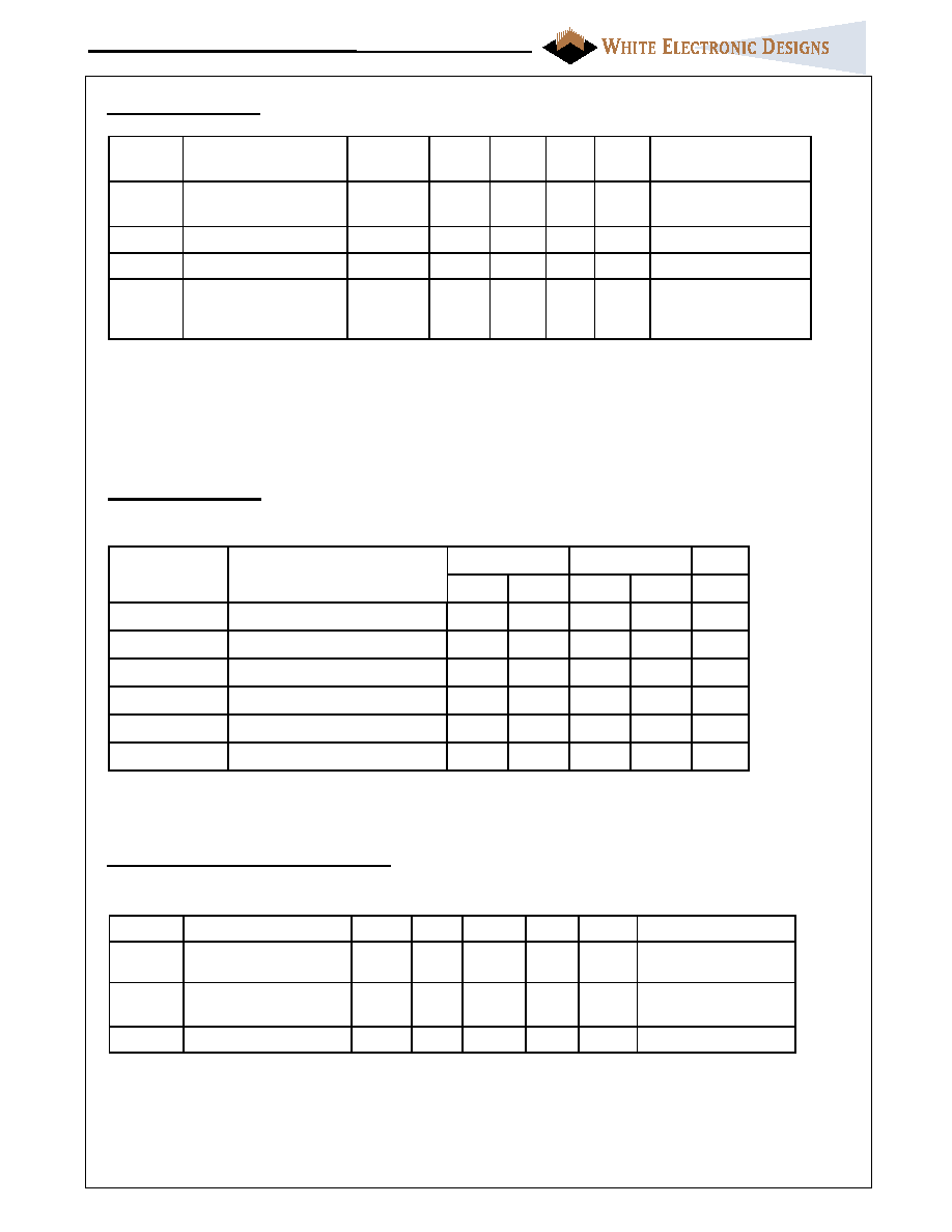
Symbol
Parameter
100 ns
150 ns
Min
Max
Min
Max
Unit
t
C
(R)
Read Cycle Time
100
150
ns
ta(A)
Address Access Time
100
150
ns
ta(CE)
Card Enable Access Time
100
150
ns
ta(OE)
Output Enable Access Time
50
75
ns
tcW
Write Cycle Time
100
150
ns
tW(WE)
Write Pulse Width
60
80
ns
VCC = 5V ± 5%, TA = 0
∞
C to + 70
∞
C
Note: AC timing diagrams and characteristics are guaranteed to meet or exceed PCMCIA 2.1 specifications.
Symbol
Parameter
Notes
Min
Typ(1)
Max
Units
Test Conditions
tWHQV1
tEHQV1
Byte Program time
2,4
7
1000
µs
tWHQV2
tEHQV2
Block Program Time
2
0.15
0.7
sec
Word Program Mode
Block Erase Time
2
1
15
sec
VCC = 5V ± 5%, TA = 0
∞
C to + 70
∞
C
Notes:
1. Typical: Nominal voltages and TA = 25
∞
C.
2. Excludes system overhead.
3. Valid for all speed options.
4. To maximize system performance RDY/BSY# signal should be polled.
5. Chip erase time based on 8 Mbit Flash components.
Symbol
Parameter
Density
(MBytes)
Notes
Typ
3
)
Max
Units
Test Conditions
ICCR
VCC Read Current
1,2,4,8
30
mA
VCC = 5.25V
tcycle = 100ns
ICCW
VCC Program Current
1,2,4,8
60
mA
ICCE
VCC Erase Current
1,2,4,8
60
mA
ICCS
VCC Standby Current
1,2,4,8
2)
20
50
µA
VCC = 5.25V
Control Signals = VCC
Reset = X
Notes:
1. All currents are RMS values unless otherwise specified.
2. Control Signals: CE1#, CE2#, OE#, WE#.
3. Typical: VCC = 5V, T = +25
∞
C.
CMOS Test Conditions: VIL = VSS ± 0.2V, VIH = VCC ± 0.2V
DC Characteristics
(1)
AC Characteristics
(1)
Data Write and Erase Performance
(1 ,3)

August 2000 Rev. 3 - ECO #13124
5
PCMCIA Flash Memory Card
FEB Series
PC Card Products
EDI
Company Name
Lot code / trace number
Date code
Part number
PRODUCT MARKING
WED
7P008FEB0500C15 C995 9915
Note:
Some products are currently marked with our pre-merger company name/acronym (EDI). During our
transition period, some products will also be marked with our new company name/acronym (WED).
Starting October 2000 all PCMCIA products will be marked only with the WED prefix.
Card capacity
008 8MB
Packaging option
00
Standard, type 1
PC card
P
Standard PCMCIA
R
Ruggedized PCMCIA
Card family and version
- See Card Family and Version Info. for details (next page)
Temperature range
C Commercial 0∞C to +70∞C
I Industrial -40∞C to +85∞C
Card access time
15
150ns
25
250ns
Card technology
7
FLASH
8
SRAM
PART NUMBERING
7
P
008
FEB05
00
C
15
August 2000 Rev. 3 - ECO #13124
6
PCMCIA Flash Memory Card
FEB Series
PC Card Products
Eight Bit Flash Memory Card
7P XXX FEB YY 00 T ZZ
where
XXX:
001
1MB (03 only)
002
2MB (03, 05)
004
4MB (03, 05)
008
8MB (05 only)
YY:
03
29F080 base
05
29F016 base
T:
C
Commercial
I
Industrial
M
Military Temp
ZZ:
10
100ns
15
150ns
Ordering Information
White Electronic Designs Corporation
One Research Drive, Westborough, MA 01581, USA
tel:
(508) 366 5151
fax: (508) 836 4850
www.whiteedc.com
Revision history:
rev level
description
date
rev 0
initial release
Feb 2, 1998
rev 1
Logo change
May 27, 1999
rev 2
Added page 5
June 1, 2000
Page Header change
rev 3
Corrected Errors on pg. 4
August 1, 2000