1
White Electronic Designs Corporation (508) 485-4000 www.whiteedc.com
White Electronic Designs
PCMCIA Flash Memory Card
FLA Series
January 2003 Rev. 5
ECO #15915
PCMCIA Flash Memory Card
1 MEGABYTE through 40 MEGABYTE (Intel/Sharp based)
FEATURES
n
Low cost High Density Linear Flash Card
n
Supports 5V only systems or 5V systems with
12V VPP
n
Based on Intel/Sharp FlashFile Components
n
Fast Read Performance
- 150ns or 200ns Maximum Access Time
n
x8 / x16 Data Interface
n
High Performance Random Writes
- 8µs Typical Word Write Time
n
Automated Write and Erase Algorithms
- Command User Interface
n
100,000 Erase Cycles per Block
n
64K word symmetrical Block Architecture
n
PC Card Standard Type I Form Factor
GENERAL DESCRIPTION
WEDCs FLA Series Flash memory cards offer high den-
sity linear Flash solid state storage solutions for code
and data storage, high performance disk emulation and
execute in place (XIP) applications in mobile PC and
dedicated (embedded) equipment.
FLA series cards conform to PCMCIA international standard.
The cards control logic provides the system interface
and controls the internal Flash memories. Card can be
read/written in byte-wide or word-wide mode which al-
lows for flexible integration into various systems. Com-
bined with file management software, such as Flash
Translation Layer (FTL), FLA Flash cards provide remov-
able high-performance disk emulation.
The FLA series offers low power modes controlled by
registers. Standard cards contain separate 2kB EEPROM
memory for Card Information Structure (CIS) which can
be used for easy identification of card characteristics.
The WEDC FLA series is based on Intel/Sharp Flash
memories.
Note: Standard options include attribute memory. Cards without
attribute memory are available. Cards are also available with or without
a hardware write protect switch.
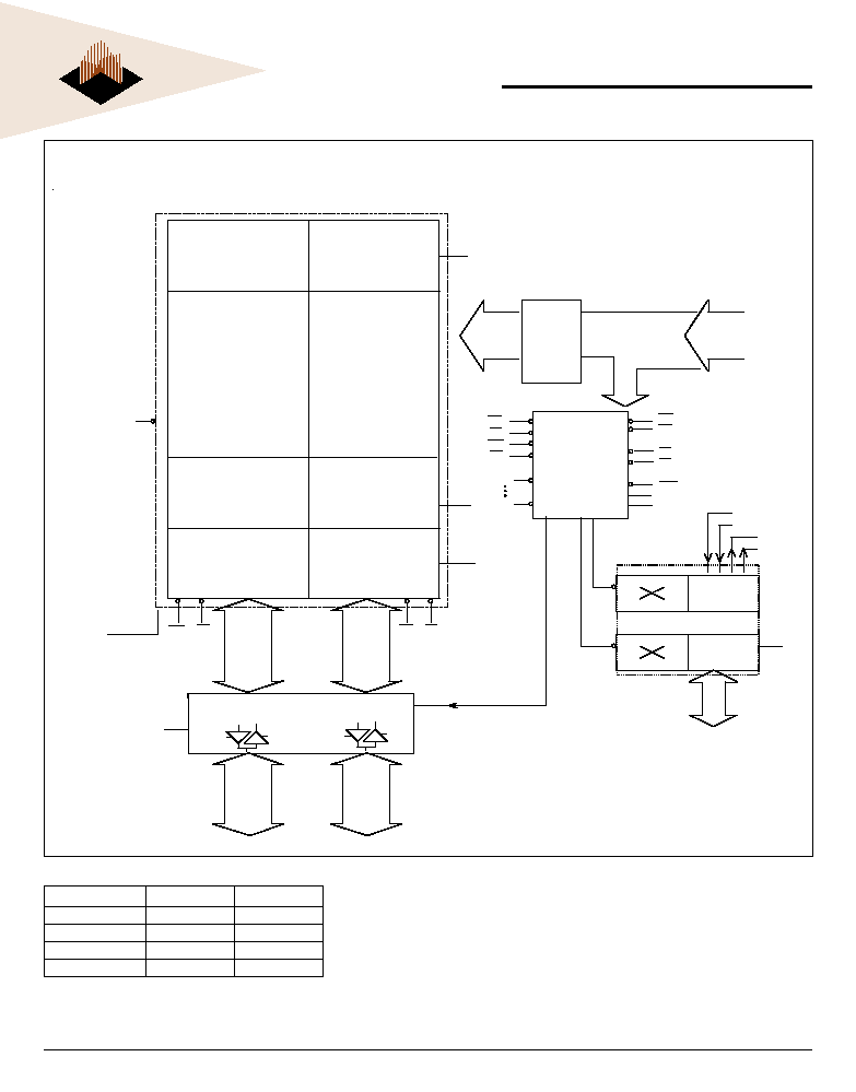
ARCHITECTURE OVERVIEW
WEDCs FLA series is designed to support from 2 to
20, 4Mb, 8Mb or 16Mb components, providing a wide
range of density options. Cards are based on the
28F008SA (8Mb) for 12V VPP applications or on the
28F004S5 (4Mb), 28F008S5 (8Mb) and 28F016S5
(16Mb) devices for 5V only applications. Devices codes
for the 28F004S5, 28F008SA, 28F008S5 and the
28F016S5 are: A7H, A2H, A6H and AAh respectively.
Systems should be able to recognize all four codes.
Cards utilizing the 8Mb components provide densities
ranging from 2MB to 20MB in 2MB increments, cards
utilizing 16Mb components provide densities ranging
from 4MB to 40MB in 4MB increments. 4 Mbit memory
devices are used only for smallest capacity cards (1MB).
In support of the PC Card 95 standard for word wide
access devices are paired. Therefore, the Flash array
is structured in 64K word (128kBytes) blocks. Write,
read and block erase operations can be performed as
either a word or byte wide operation . By multiplexing A
0
,
CE
1
and CE
2
, 8-bit hosts can access all data on data
lines DQ
0
-DQ
7
.
The FLA21-FLA36 series also supports the following
PCMCIA compatible register functions: Soft Reset via the
Configuration Option Register, Power Down (sleep mode)
via the Configuration and Status Register and monitoring
of Ready/Busy, Soft Reset and Power Down via the Card
Status Register (cards without attribute memory and ver-
sions FLA51 - FLA66 do not have registers).
The FLA series cards conform with the PC Card Stan-
dard (PCMCIA) and JEIDA, providing electrical and physi-
cal compatibility. The PC Card form factor offers an in-
dustry standard pinout and mechanical outline, allow-
ing density upgrades without system design changes.
WEDCs standard cards are shipped with WEDCs
Logo. Cards are also available with blank housings
(no Logo). The blank housings are available in both a
recessed (for label) and flat housing. Please contact
WEDC sales representative for further information on
Custom artwork.
3
White Electronic Designs Corporation (508) 485-4000 www.whiteedc.com
White Electronic Designs
PCMCIA Flash Memory Card
FLA Series
ADDRESS
REGISTER NAME
4100h
Status Register
4002h
Config. and Status Register
4000h
Configuration Option Register
R
EGISTERS
IN
A
TTRIBUTE
M
EMORY
S
PACE
*
COR
C
ONFIGURATION
O
PTION
R
EGISTER
: ADRS = 4000h
W
RITE
O
NLY
*Cards without Att. Mem and FLA51- FLA66 do
not have registers
SRES
LREQ
Configuration Index
D7
D6
D5
D4
D3
D2
D1
D0
D7
Soft Reset, active High
1 = Reset State
0 = End Reset State
D6
Level Req (not supported)
D5-D0 Configuration index (not supported)
CSR
C
ONFIGURATION
S
TATUS
R
EGISTER
: ADRS = 4002h
W
RITE
O
NLY
Not Supported
PDwn Not Supported
D7
D6
D5
D4
D3
D2
D1
D0
D2
Power Down, active High
1 = Place all memory devices in power down mode
0 = Normal Operation
Power On default = 0
SR
S
TATUS
R
EGISTER
: ADRS = 4100h
R
EAD
O
NLY
Not Supported
SReset
PDwn
Not Supported R/BSY
D7
D6
D5
D4
D3
D2
D1
D0
D5
Represents the state of SRESET bit in COR (4000h)
1 = Reset
0 = Normal Operation
Power On default D5 = 0
D3
Represents the state of Power Down bit (D2) in CSR (4002h)
1 = Power Down
D0
Reflects the card's Ready/Busy signal (pin 16) driven by
memory components Ready/Busy outputs. This bit allows
software polling of the card's Ready/Busy status.
1 = Ready
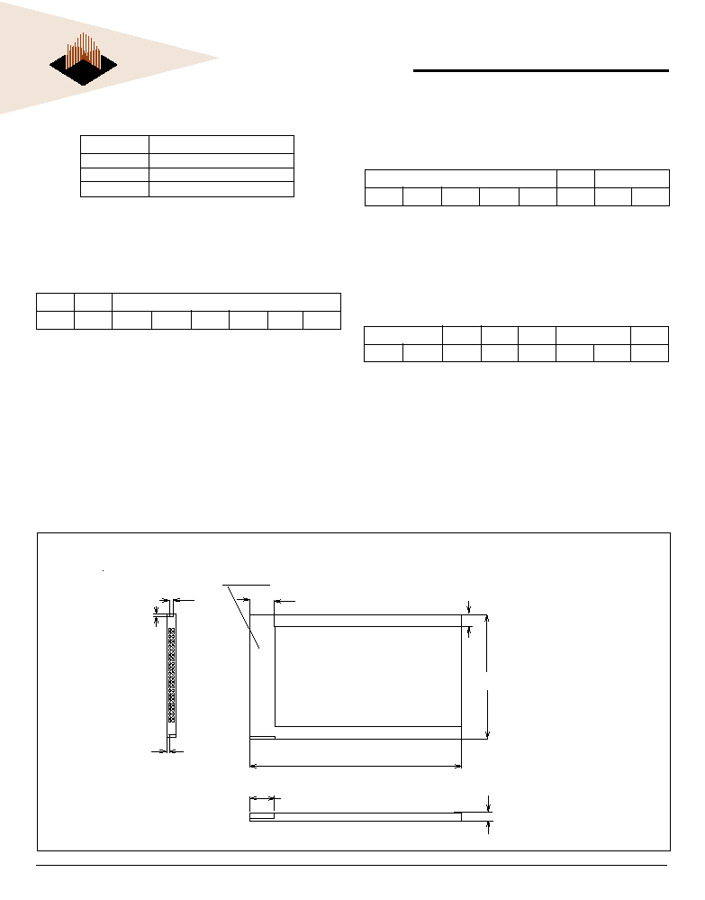
54.0mm
±
0.10
(2.126")
10.0mm MIN
(0.400")
1.6mm
±
0.05
(0.063")
1.0mm
±
0.05
(0.039")
1.0mm
±
0.05
(0.039")
3.3mm
±
T1 (0.130")
T1=0.10mm interconnect area
T1=0.20mm substrate area
Interconnect area
10.0mm MIN
(0.400")
3.0mm MIN
85.6mm
±
0.20
(3.370")
Substrate area
MECHANICAL
5
White Electronic Designs Corporation (508) 485-4000 www.whiteedc.com
White Electronic Designs
PCMCIA Flash Memory Card
FLA Series
Symbol
Type
Name and Function
A
0
- A
25
INPUT
ADDRESS INPUTS: A
0
through A
25
enable direct addressing of up to 64MB of memory on the
card. Signal A
0
is not used in word access mode. A
25
is the most significant bit
DQ
0
- DQ
15
INPUT/OUTPUT
DATA INPUT/OUTPUT: DQ
0
THROUGH DQ
15
constitute the bi-directional databus. DQ
15
is the MSB.
CE
1
, CE
2
INPUT
CARD ENABLE 1 AND 2: CE
1
enables even byte accesses, CE
2
enables odd byte accesses.
Multiplexing A
0
, CE
1
and CE
2
allows 8-bit hosts to access all data on DQ
0
- DQ
7
.
OEINPUT
OUTPUT ENABLE: Active low signal gating read data from the memory card.
WEINPUT
WRITE ENABLE: Active low signal gating write data to the memory card.
RDY/BSY(*)
OUTPUT
READY/BUSY OUTPUT: Indicates status of internally timed erase or program algorithms. A high
output indicates that the card is ready to accept accesses. A low output indicates that one or more
devices in the memory card are busy with internally timed erase or write activities.
CD
1
, CD
2
OUTPUT
CARD DETECT 1 and 2: Provide card insertion detection. These signals are internally connected
to ground on the card. The host shall monitor these signals to detect card insertion (pulled-up on
host side).
WP
OUTPUT
WRITE PROTECT: Write protect reflects the status of the Write Protect switch on the memory
card. WP set to high = write protected, providing internal hardware write lockout to the Flash
array.If card does not include optional write protect switch, this signal will be pulled low internally
indicating write protect = off.
V
PP
1
, V
PP
2
N.C.
PROGRAM/ERASE POWER SUPPLY: Provides programming voltages for card (12V). Not
connected for 5V only card.
V
CC
CARD POWER SUPPLY: (5.0V).
GND
CARD GROUND
REG
INPUT
ATTRIBUTE MEMORY SELECT : Active low signal, enables access to Attribute Memory Plane,
occupied by Card Information Structure and Card Registers.
RST(*)
INPUT
RESET: Active high signal for placing card in Power-on default state. Reset can be used as a
Power-Down signal for the memory array.
WAIT(*)
OUTPUT
WAIT: This signal is pulled high internally for compatibility. No wait states are generated.
BVD1, BVD2
OUTPUT
BATTERY VOLTAGE DETECT: These signals are pulled high to maintain SRAM card compatibility.
VS
1
, VS
2
OUTPUT
VOLTAGE SENSE: Notifies the host socket of the cards V
CC
requirements. VS
1
and VS
2
are
open to indicate a 5V card .
RFU
RESERVED FOR FUTURE USE
NC
NO INTERNAL CONNECTION TO CARD: pin may be driven or left floating
C
ARD
S
IGNAL
D
ESCRIPTION
(*) Signals not supported by FLA51-66 (N.C)
READ function
Common Memory
Attribute Memory
Function Mode
CE
2
CE
1
A
0
OE
WE
REG
D
15
-D
8
D
7
-D
0
REG
D
15
-D
8
D
7
-D
0
Standby Mode
H
H
X
X
X
X
High-Z
High-Z
X
High-Z
High-Z
Byte Access (8 bits)
H
L
L
L
H
H
High-Z
Even-Byte
L
High-Z
Even-Byte
H
L
H
L
H
H
High-Z
Odd-Byte
L
High-Z
Not Valid
Word Access (16 bits)
L
L
X
L
H
H
Odd-Byte
Even-Byte
L
Not Valid
Even-Byte
Odd-Byte Only Access
L
H
X
L
H
H
Odd-Byte
High-Z
L
Not Valid
High-Z
WRITE function
Standby Mode
H
H
X
X
X
X
X
X
X
X
X
Byte Access (8 bits)
H
L
L
H
L
H
X
Even-Byte
L
X
Even-Byte
H
L
H
H
L
H
X
Odd-Byte
L
X
X
Word Access (16 bits)
L
L
X
H
L
H
Odd-Byte
Even-Byte
L
X
Even-Byte
Odd-Byte Only Access
L
H
X
H
L
H
Odd-Byte
X
L
X
X
F
UNCTIONAL
T
RUTH
T
ABLE