
1
White Electronic Designs Corporation (508) 485-4000 www.whiteedc.com
White Electronic Designs
PCMCIA Flash Memory Card
FLD Series
March 2003 Rev. 6
ECO #16058
PCMCIA Flash Memory Card - 4 MEGABYTE through
40 MEGABYTE (AMD based)
GENERAL DESCRIPTION
WEDCs PCMCIA Flash memory cards offer high den-
sity linear Flash solid state storage solutions for code
and data storage, high performance disk emulation and
execute in place (XIP) applications in mobile PC and
dedicated (embedded) equipment.
Packaged in a PCMCIA type I housing, each card con-
tains a connector, an array of Flash memories pack-
aged in TSOP packages and card control logic. The
card control logic provides the system interface and
controls the internal Flash memories. Combined with
file management software, such as Flash Translation
Layer (FTL), WEDC Flash cards provide removable high-
performance disk emulation.
The WEDC FLD series is based on AMD Flash
memo-
ries. The FLD series offers byte wide and word wide
operation, low power modes and Card Information Struc-
ture (CIS) for easy identification of card characteristics.
Note:
Standard options include attribute memory. Cards without attribute
memory are available. Cards are also available with or without a
hardware write protect switch.
FEATURES
n
Low cost High Density Linear Flash Card
n
Supports 5V only systems
n
Based on AMD Am29F017 Flash Components
- low standby power without entering reset mode
- allows standard access from standby mode
n
Fast Read Performance
- 150ns Maximum Access Time
n
x8/ x16 Data Interface
n
High Performance Random Writes
- 7�s typical Word Write Time
n
Automated Write and Erase Algorithms
- AMD Command Set
n
1 000,000 Erase Cycles per Block
n
64K word (128kB) symmetrical Block Architecture
n
PC Card Standard Type I Form Factor
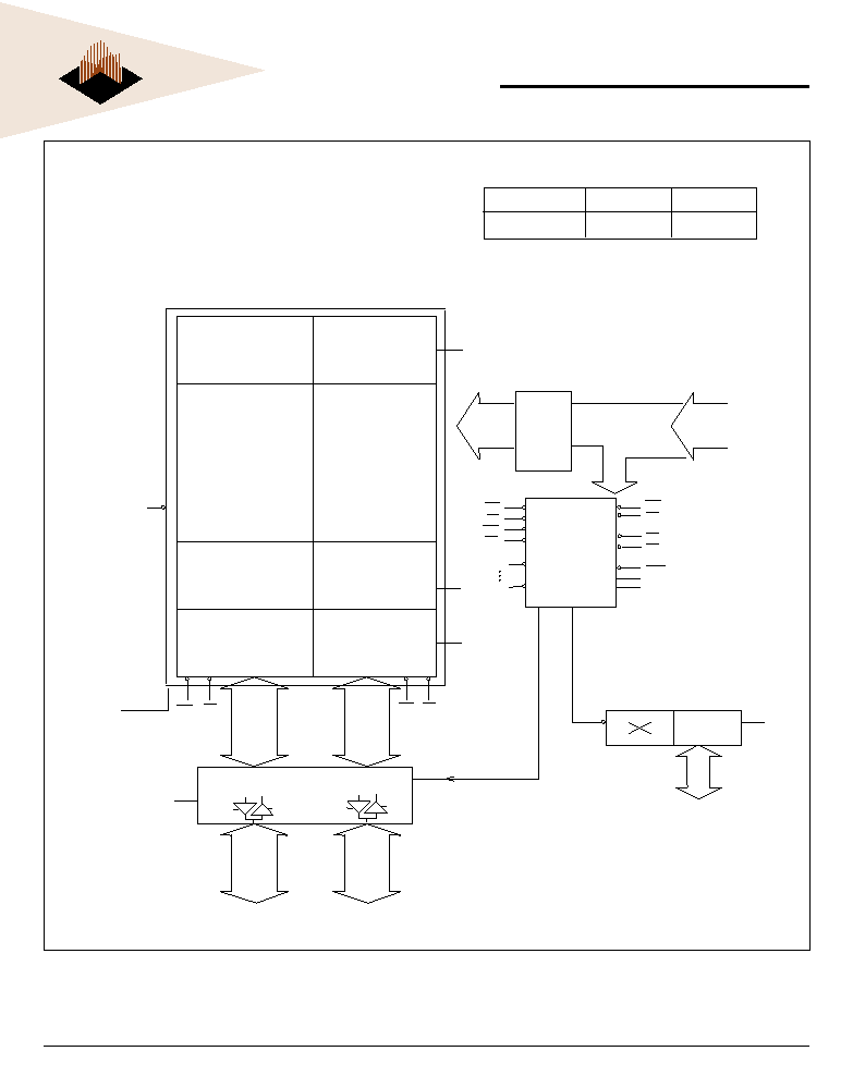
ARCHITECTURE OVERVIEW
WEDCs FLD series is designed to support from two to
twenty (see Block diagram) 16Mb components, provid-
ing a wide range of density options. Cards are based
on the Am29F017 (16Mb) device for 5V only applica-
tions. The device code for the Am29F017 is 3Dh and the
manufacturers ID is 01h. This card is compatible with
D series cards from AMD. Cards utilizing 16Mb compo-
nents provide densities ranging from 4MB to 40MB in
4MB increments.
In support of the PC Card (PCMCIA) standard for word
wide access, devices are paired. Therefore, the Flash
array is structured in 64K word (128kB)blocks. Write,
read operations can be performed as either a word or
byte wide operation. By multiplexing A0, CE1# and CE2#,
8-bit hosts can access all data on data lines DQ0 -
DQ7. The FLD series cards conform with the PC Card
Standard (formerly PCMCIA) and supported JEIDA, pro-
viding electrical and physical compatibility. The PC Card
form factor offers an industry standard pinout and me-
chanical outline, allowing density upgrades without sys-
tem design changes.
WEDCs standard cards are shipped with WEDCs
silkscreen design. Cards are also available with blank
housings (no silkscreen). The blank housings are avail-
able in both a recessed (for label) and flat housing.
Please contact your WEDC sales representative for fur-
ther information on Custom artwork.
2
White Electronic Designs Corporation Marlborough MA (508) 485-4000
PCMCIA Flash Memory Card
FLD Series
White Electronic Designs
BLOCK DIAGRAM
Vcc
CSn
Device Pair (N/2 - 1)
RH
I/O buffer
M Res
WH
DATA
BUS
D
8
-D
15
Vcc
0000h
WL
RL
Q
0
-Q
7
WH
WL
CSn
RL
RH
Q2
Qn
At/Reg enable
CS
0
Q0
Control Logic
PCMCIA Interface
Ctrl
attrib. mem
CIS
EEPROM 2kB
WE
OE
CE
2
CE
1
REG
A
0
WP
ADDRESS BUS
ADDRESS
BUFFER
Array
Address
Bus
A
1
-A
25
DATA
BUS
D
0
-D
7
DATA
BUS
Q
0
-Q
7
DATA
BUS
Q
8
-Q
15
Vcc
control
Device (N-1)
Device (N-2)
Device 3
Device 2
Device 1
Device 0
CS
1
CS
0
Control
Address
Bus
Device Pair 1
Device Pair 0
Device type
Manuf ID
Device ID
Am29F017
01
H
3D
H
3
White Electronic Designs Corporation (508) 485-4000 www.whiteedc.com
White Electronic Designs
PCMCIA Flash Memory Card
FLD Series
Pin
Signal name
I/O
Function
Active
1
GND
Ground
2
DQ
3
I/O
Data bit 3
3
DQ
4
I/O
Data bit 4
4
DQ
5
I/O
Data bit 5
5
DQ
6
I/O
Data bit 6
6
DQ
7
I/O
Data bit 7
7
CE
1
I
Card enable 1
LOW
8
A
10
I
Address bit 10
9
OE
I
Output enable
LOW
10
A
11
I
Address bit 11
11
A
9
I
Address bit 9
12
A
8
I
Address bit 8
13
A
13
I
Address bit 13
14
A
14
I
Address bit 14
15
WE
I
Write Enable
LOW
16
RDY/BSY
O
Ready/Busy
LOW
17
V
CC
Supply Voltage
18
V
PP
1
Prog. Voltage
N.C.
19
A
16
I
Address bit 16
20
A
15
I
Address bit 15
21
A
12
I
Address bit 12
22
A
7
I
Address bit 7
23
A
6
I
Address bit 6
24
A
5
I
Address bit 5
25
A
4
I
Address bit 4
26
A
3
I
Address bit 3
27
A
2
I
Address bit 2
28
A
1
I
Address bit 1
29
A
0
I
Address bit 0
30
DQ
0
I/O
Data bit 0
31
DQ
1
I/O
Data bit 1
32
DQ
2
I/O
Data bit 2
33
WP
O
Write Potect
HIGH
34
GND
Ground
Pin
Signal name
I/O
Function
Active
35
GND
Ground
36
CD
1
O
Card Detect 1
LOW
37
DQ
11
I/O
Data bit 11
38
DQ
12
I/O
Data bit 12
39
DQ
13
I/O
Data bit 13
40
DQ
14
I/O
Data bit 14
41
DQ
15
I
Data bit 15
42
CE
2
I
Card Enable 2
LOW
43
VS
1
O
Voltage Sense 1N.C.
44
RFU
Reserved
45
RFU
Reserved
46
A
17
I
Address bit 17
47
A
18
I
Address bit 18
48
A
19
I
Address bit 19
49
A
20
I
Address bit 20
2MB(3)
50
A
21
I
Address bit 21
4MB(3)
51
V
CC
Supply Voltage
52
V
PP
2
Prog. Voltage
N.C.
53
A
22
I
Address bit 22
8MB(3)
54
A
23
I
Address bit 23
16MB(3)
55
A
24
I
Address bit 24
32MB(3)
56
A
25
I
Address bit 25
64MB(3)
57
VS
2
O
Voltage Sense 2
N.C.
58
RST
I
Card Reset
HIGH
59
Wait
O
Extended Bus cycle
LOW(2)
60
RFU
Reserved
61
REG
I
Attrib Mem Select
62
BVD
2
O
Bat. Volt. Detect 2
(2)
63
BVD
1
O
Bat. Volt. Detect 1
(2)
64
DQ
8
I/O
Data bit 8
65
DQ
9
I/O
Data bit 9
66
DQ
10
O
Data bit 10
67
CD
2
O
Card Detect 2
LOW
68
GND
Ground
P
INOUT
P
INOUT
CONT
.
Notes:
1. RDY/BSY is an open drain output, external pull-up resistor is required.
2. Wait, BVD
1
and BVD
2
are driven high for compatibility.
3. Shows density for which specified address bit is MSB.
Higher order address bits are no connects (ie 4MB A
21
is MSB A
22
- A
25
are NC).
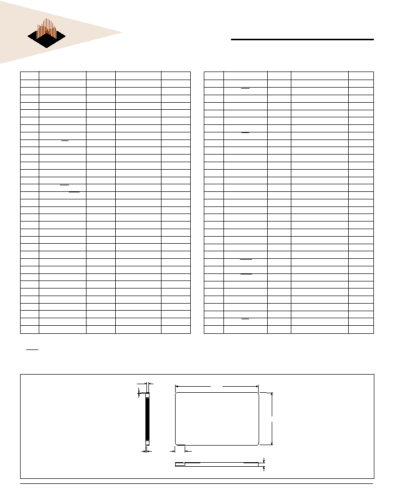
MECHANICAL
3.370
2.126
.039
.063
.400
.130
.039
4
White Electronic Designs Corporation Marlborough MA (508) 485-4000
PCMCIA Flash Memory Card
FLD Series
White Electronic Designs
C
ARD
S
IGNAL
D
ESCRIPTION
Symbol
Type
Name and Function
A
0
- A
25
INPUT
ADDRESS INPUTS: A
0
through A
25
enable direct addressing of up to 64MB of memory
on the card. Signal A
0
is not used in word access mode. A
25
is the most significant bit
DQ
0
- DQ
15
INPUT/OUTPUT
DATA INPUT/OUTPUT: DQ
0
THROUGH DQ
15
constitute the bi-directional databus.
DQ15 is the MSB.
CE
1
, CE
2
INPUT
CARD ENABLE 1 AND 2: CE
1
enables even byte accesses, CE
2
enables odd byte
accesses. Multiplexing A
0
, CE
1
and CE
2
allows 8-bit hosts to access all data on DQ
0
- DQ
7
.
OE
INPUT
OUTPUT ENABLE: Active low signal gating read data from the memory card.
WE
INPUT
WRITE ENABLE: Active low signal gating write data to the memory card.
RDY/BSY
OUTPUT
READY/BUSY OUTPUT: Indicates status of internally timed erase or program algorithms.
A high output indicates that the card is ready to accept accesses. A low output indicates
that one or more devices in the memory card are busy with internally timed erase or
write activities.
CD
1
, CD
2
OUTPUT
CARD DETECT 1 and 2: Provide card insertion detection. These signals are connected
to ground internally on the memory card. The host socket interface circuitry shall supply
10K-ohm or larger pull-up resistors on these signal pins.
WP
OUTPUT
WRITE PROTECT: Write protect reflects the status of the Write Protect switch on the
memory card. WP set to high = write protected, providing internal hardware write lockout
to the Flash array.If card does not include optional write protect switch, this signal will be
pulled low internally indicating write protect = off.
V
PP
1
, V
PP
2
N.C.
PROGRAM/ERASE POWER SUPPLY: Not connected for 5V only card.
V
CC
CARD POWER SUPPLY: 5.0V for all internal circuitry.
GND
GROUND: for all internal circuitry.
REG
INPUT
ATTRIBUTE MEMORY SELECT : provides access to Flash memory card registers and
Card Information Structure in the Attribute Memory Plane.
RST
INPUT
RESET: Active high signal for placing card in Power-on default state. Reset can be used
as a Power-Down signal for the memory array.
WAIT
OUTPUT
WAIT: This signal is pulled high internally for compatibility. No wait states are generated.
BVD
1
, BVD
2
OUTPUT
BATTERY VOLTAGE DETECT: These signals are pulled high to maintain SRAM card
compatibility.
VS
1
, VS
2
OUTPUT
VOLTAGE SENSE: Notifies the host socket of the cards V
CC
requirements. VS
1
and
VS
2
are open to indicate a 5V card has been inserted.
RFU
RESERVED FOR FUTURE USE
N.C.
NO INTERNAL CONNECTION TO CARD: pin may be driven or left floating
A
BSOLUTE
M
AXIMUM
R
ATINGS
(2)
Operating Temperature TA (ambient)
Commercial
0�C to +60 �C
Industrial
-40�C to +85 �C **
Storage Temperature
Commercial
-30�C to +80 �C
Industrial
-40�C to +85 �C **
Voltage on any pin relative to V
SS
-0.5V to V
CC
+0.5V (1)
V
CC
supply Voltage relative to V
SS
-0.5V to +7.0V
** Advanced information
Notes:
(1) During transitions, inputs may undershoot to -2.0V or overshoot to V
CC
+2.0V for periods less than 20ns.
(2) Stress greater than those listed under Absolute Maximum ratings may cause permanent damage to the device.
This is a stress rating only and functional operation at these or any other conditions greater than those indicated in
the operational sections of this specification is not implied. Exposure to absolute maximum rating conditions for
extended periods may affect reliability.

5
White Electronic Designs Corporation (508) 485-4000 www.whiteedc.com
White Electronic Designs
PCMCIA Flash Memory Card
FLD Series
DC C
HARACTERISTICS
(1)
Sym
Parameter
Density
Notes
Typ
(4)
Max
Units
Test Conditions
(Mbytes)
I
CCR
V
CC
Read Current
All
75
mA
V
CC
= 5V +/- 10%
tcycle = 150ns
I
CCW
V
CC
Program Current
All
150
mA
I
CCE
V
CC
Erase Current
All
150
mA
I
CCS
V
CC
Standby Current
2MB
2,3
80
230
�AV
CC
= 5V +/- 10%
(4MB)
Control Signals = V
IL
or V
OH
Reset = V
SS
Test Conditions: V
CC
= 5V � 10%, V
I
= V
IL
or V
IH
Notes:
1. All currents are RMS values unless otherwise specified. I
CCR
, I
CCW
and I
CCE
are based on Word wide operations.
2. Control Signals: CE
1
, CE
2
, OE, WE, REG.
3. I
CCD
and I
CCS
are specified for lowest density card for each component type (2MB for 8Mb components and 4MB for 16Mb components) This
represents a single pair of devices. For higher densities multiply the number of device pairs by the specified current in the table. For example a
40MB card will use 10 device pairs of 16Mb components. The maximum I
CCD
will be 10 x 40�A = 400�A. The maximum I
CCS
will be
10 x 230�A = 2.3mA.
4. Typical: V
CC
= 5V, T = +25�C.
Symbol
Parameter
Notes
Min
Max
Units
Test Conditions
I
LI
Input Leakage Current
1
�20
�AV
CC
= 5V +/- 10%
V
IN
=V
CC
or V
SS
I
LO
Output Leakage Current
1
�20
�AV
CC
= 5V +/- 10%
V
OUT
=V
CC
or V
SS
V
IL
Input Low Voltage
1
0
0.8
V
V
IH
Input High Voltage
1
2
V
V
OL
Output Low Voltage
1
0.26
V
I
OL
= 4mA
V
OH
Output High Voltage
1
3.98
V
I
OH
= -4mA
V
LKO
V
CC
Erase/ProgramLock Voltage
1
3.2
4.2
V
Notes:
1. Values are the same for byte and word wide modes for all card densities.
2. Exceptions: Leakage currents on CE
1
, CE
2
, OE, REG and WE will be < 500 �A when V
IN
= GND due to internal pull-up resistors. Leakage
currents on RST will be <150�A when V
IN
=V
CC
due to internal pull-down resistor.

6
White Electronic Designs Corporation Marlborough MA (508) 485-4000
PCMCIA Flash Memory Card
FLD Series
White Electronic Designs
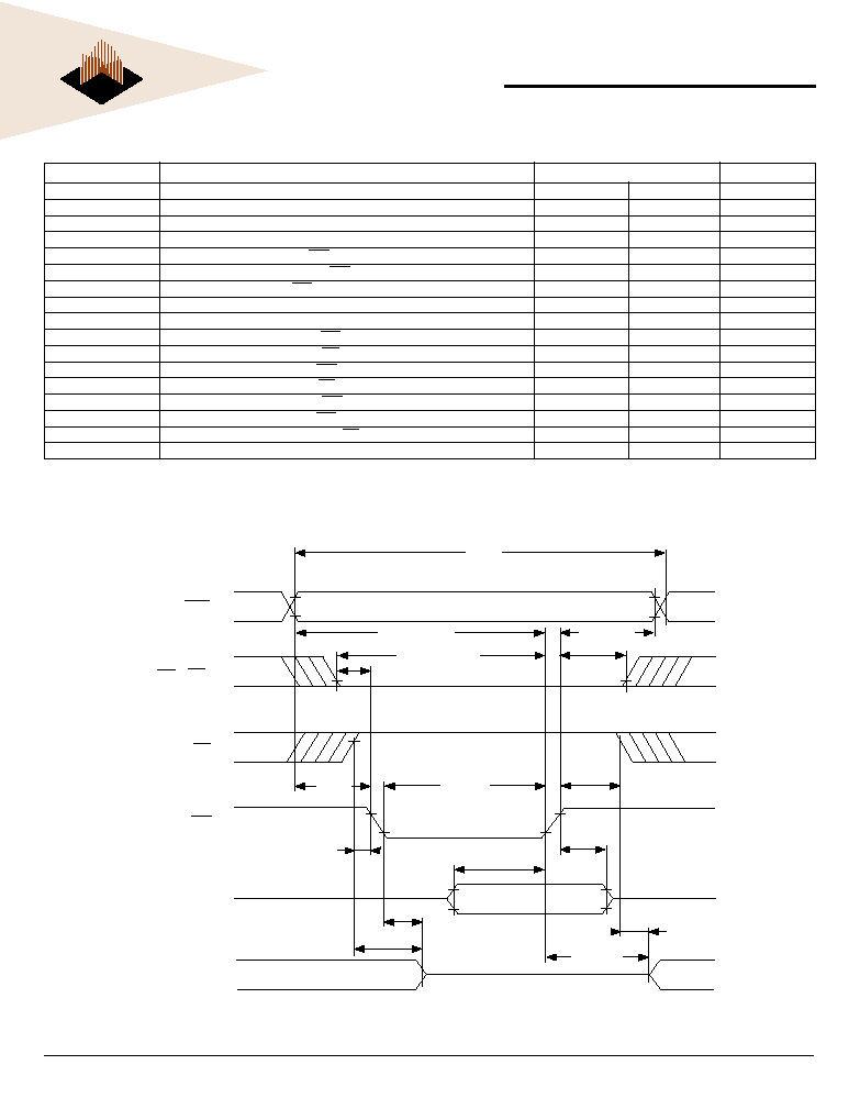
AC CHARACTERISTICS
150ns
SYM (PCMCIA)
Parameter
Min
Max
Unit
t
C
(R)
Read Cycle Time
150
ns
t
a
(A)
Address Access Time
150
ns
t
a
(CE)
Card Enable Access Time
150
ns
t
a
(OE)
Output Enable Access Time
75
ns
t
su
(A)
Address Setup Time
20
ns
t
su
(CE)
Card Enable Setup Time
0
ns
t
h
(A)
Address Hold Time
20
ns
t
h
(CE)
Card Enable Hold Time
20
ns
t
v
(A)
Output Hold from Address Change
0
ns
t
dis
(CE)
Output Disable Time from CE
75
ns
t
dis
(OE)
Output Disable Time from OE
75
ns
t
en
(CE)
Output Enable Time from CE
5
ns
t
en
(OE)
Output Enable Time from OE
5
ns
Note: AC timing diagrams and characteristics are guaranteed to meet or exceed PCMCIA 2.1 specifications.
R
EAD
T
IMING
P
ARAMETERS
R
EAD
T
IMING
D
IAGRAM
A[25::0], REG
t
C
(R)
CE
1
, CE
2
OE
D[15::0]
t
A
(CE)
t
H
(A)
t
SU
(A)
NOTE 1
DATA VALID
t
A
(A)
t
V
(A)
t
SU
(CE)
NOTE 1
t
A
(OE)
t
H
(CE)
t
EN
(OE)
t
DIS
(CE)
t
DIS
(OE)
Note: Signal may be high or low in this area.
7
White Electronic Designs Corporation (508) 485-4000 www.whiteedc.com
White Electronic Designs
PCMCIA Flash Memory Card
FLD Series
150ns
SYM (PCMCIA)
Parameter
Min
Max
Unit
t
C
W
Write Cycle Time
150
ns
t
w
(WE)
Write Pulse Width
80
ns
t
su
(A)
Address Setup Time
20
ns
t
su
(A-WEH)
Address Setup Time for WE
100
ns
t
su
(CE-WEH)
Card Enable Setup Time for WE
100
ns
t
su
(D-WEH)
Data Setup Time for WE
50
ns
t
h
(D)
Data Hold Time
20
ns
t
rec
(WE)
Write Recover Time
20
ns
t
dis
(WE)
Output Disable Time from WE
75
ns
t
dis
(OE)
Output Disable Time from OE
75
ns
t
en
(WE)
Output Enable Time from WE
5
ns
t
en
(OE)
Output Enable Time from OE
5
ns
t
su
(OE-WE)
Output Enable Setup from WE
10
ns
t
h
(OE-WE)
Output Enable Hold from WE
10
ns
t
su
(CE)
Card Enable Setup Time from OE
0
ns
t
h
(CE)
Card Enable Hold Time
20
ns
Note: AC timing diagrams and characteristics are guaranteed to meet or exceed PCMCIA 2.1 specifications.
W
RITE
T
IMING
P
ARAMETERS
W
RITE
T
IMING
D
IAGRAM
A[25::0], REG
t
C
(W)
CE
1
, CE
2
OE
D[15::0](D
IN
)
t
W
(WE)
t
SU
(A)
NOTE 1
DATA INPUT
t
SU
(A-WEH)
t
SU
(CE)
NOTE 1
t
REC
(WE)
t
H
(CE)
t
SU
(OE-WE)
t
H
(D)
t
EN
(WE)
D[15::0](D
OUT
)
WE
t
SU
(CE-WEH)
t
H
(OE-WE)
t
DIS
(OE)
t
DIS
(WE)
NOTE 2
NOTE 2
t
SU
(D-WEH)
t
EN
(OE)
Notes: 1. Signal may be high or low in this area.
2. When the data I/O pins are in the output state, no signals shall be applied to the data pins (D15 - D0) by the host system.

8
White Electronic Designs Corporation Marlborough MA (508) 485-4000
PCMCIA Flash Memory Card
FLD Series
White Electronic Designs
D
ATA
W
RITE
AND
E
RASE
P
ERFORMANCE
(1,3)
V
CC
= 5V � 5%, T
A
= 0�C
TO
+ 60�C
SYM
Parameter
Notes
Min
Typ
(1)
Max
Units
Test Conditions
t
WHQV1
t
EHQV1
Word/Byte Program time
2,4
7
300
�s
Excludes system-level overhead
t
WHQV2
t
EHQV2
Block Program Time
2
0.5
2.0
sec
Block Erase Time
2
1
8
sec
Excludes 00h prog. prior to erasure
Notes:
1. Typical: Nominal voltages and T
A
= 25�C.
2. Excludes system overhead.
3. Valid for all speed options.
4. To maximize system performance RDY/BSY signal should be polled.
P
RODUCT
M
ARKING
EDI
WED 7P016FLD2200C15 C995 9915
COMPANY NAME
PART NUMBER
LOT CODE/TRACE NUMBER
DATE CODE
7 P 016 FLD22 00 C 15
CARD TECHNOLOGY
7 FLASH
8 SRAM
PC CARD
P Standard PCMCIA
R Ruggedized PCMCIA
CARD CAPACITY
016 16MB
CARD FAMILY AND VERSION
- See Card Family and Version Info. for details (next page)
PACKAGING OPTION
00 Standard, type 1
TEMPERATURE RANGE
C = Commercial 0�C to +70�C
I = Industrial
-40�C to +85�C
CARD ACCESS TIME
15 150ns
25 250ns
P
ART
N
UMBERING

9
White Electronic Designs Corporation (508) 485-4000 www.whiteedc.com
White Electronic Designs
PCMCIA Flash Memory Card
FLD Series
XXX
004
4MB
008
8MB
012
12MB
016
16MB
020
20MB
024
24MB
028
28MB
032
32MB
036
36MB
040
40MB
SS
00 WEDC Silkscreen
01 Blank Housing, Type I
02 Blank Housing, Type I Recessed
T
C = Commercial
I
= Industrial
ZZ
15 150ns
Notes: Options without attribute memory and with hardware write protect switch are available.
O
RDERING
I
NFORMATION
7P XXX FLD22 SS T ZZ
CARD FAMILIES:
FLD 21
- No Attribute memory, No WP switch
FLD 22
- With Attribute Memory, No WP switch
FLD 23
- No Attribute Memory, With WP switch
FLD 24
- With Attribute Memory, With WP switch

10
White Electronic Designs Corporation Marlborough MA (508) 485-4000
PCMCIA Flash Memory Card
FLD Series
White Electronic Designs
ADDRESS
VALUE
DESCRIPTION
4CH
1)
x
4EH
1)
x
50H
46H
F
52H
4CH
L
54H
44H
D
56H
32H
2
58H
2)
x
5AH
2DH
-
5CH
2DH
-
5EH
2DH
-
60H
31H
1
62H
35H
5
64H
20H
SPACE
66H
00H
END TEXT
68H
43H
C
6AH
4FH
O
6CH
50H
P
6EH
59H
Y
70H
52H
R
72H
49H
I
74H
47H
G
76H
48H
H
78H
54H
T
7AH
20H
SPACE
66H
00H
END TEXT
68H
43H
C
6AH
4FH
O
6CH
50H
P
6EH
59H
Y
70H
52H
R
72H
49H
I
74H
47H
G
76H
48H
H
78H
54H
T
7AH
20H
SPACE
7CH
45H
E
7EH
4CH
L
80H
45E
E
82H
43H
C
84H
54H
T
86H
52H
R
88H
4FH
O
8AH
4EH
N
8CH
49H
I
8EH
43H
C
90H
20H
SPACE
92H
44H
D
94H
45H
E
ADDRESS
VALUE
DESCRIPTION
00H
01H
CISTPL_DEVICE
02H
03H
TPL_LINK
04H
53H
FLASH = 150ns (device writable)
06H
0EH
CARD SIZE: 4MB
1EH
8MB
2EH
12MB
3EH
16MB
4EH
20MB
5EH
24MB
6EH
28MB
7EH
32MB
8EH
36MB
9EH
40MB
08H
FFH
END OF DEVICE
0AH
18H
CISTPL_JEDEC_C
0CH
02H
TPL_LINK
0EH
01H
AMD - ID
10H
3DH
INTEL 29F017 - ID
12H
17H
CISTPL_DEVICE_A
14H
03H
TPL_LINK
16H
42H
EEPROM - 200ns
18H
01H
Device Size = 2KBytes
1AH
FFH
END OF TUPLE
1CH
1EH
CISTPL_DEVICEGEO
1EH
06H
TPL_LINK
20H
02H
DGTPL_BUS
22H
11H
DGTPL_EBS
24H
01H
DGTPL_RBS
26H
01H
DGTPL_WBS
28H
01H
DGTPL_PART
2AH
01H
FLASH DEVICE
NON-INTERLEAVED
2CH
20H
CISTPL_MANFID
2EH
04H
TPL_LINK(04H)
30H
F6H
EDI TPLMID_MANF: LSB
32H
01H
EDI TPLMID_MANF: MSB
34H
00H
LSB: Number Not Assigned
36H
00H
MSB: Number Not Assigned
38H
15H
CISTPL_VERS1
3AH
47H
TPL_LINK
3CH
04H
TPLLV1_MAJOR
3EH
01H
TPLLV1_MINOR
40H
45H
E
42H
44H
D
44H
49H
I
46H
37H
7
48H
50H
P
4AH
30H
0
CIS I
NFORMATION
FOR
FLD S
ERIES
C
ARDS
The shaded area (addresses 56H 58H) represents just some of the family versions. For all the versions see the Card Family and Version information.

11
White Electronic Designs Corporation (508) 485-4000 www.whiteedc.com
White Electronic Designs
PCMCIA Flash Memory Card
FLD Series
CIS I
NFORMATION
FOR
FLD S
ERIES
C
ARDS
(
CONT
.)
ADDRESS
VALUE
DESCRIPTION
96H
53H
S
98H
49H
I
9AH
47H
G
9CH
4EH
N
9EH
53H
S
A0H
20H
SPACE
A2H
49H
I
A4H
4EH
N
A6H
43H
C
A8H
4FH
O
AAH
52H
R
ACH
50H
P
AEH
4FH
O
B0H
52H
R
B2H
41H
A
B4H
54H
T
B6H
45H
E
B8H
44H
D
BAH
20H
SPACE
BCH
00H
END TEXT
BEH
31H
1
C0H
39H
9
C2H
39H
9
C4H
37H
7
C6H
00H
END TEXT
C8H
00H
END OF LIST
1)
Address
Value
Description
4CH
30
0
31
1
32
2
33
3
34
4
4EH
30
0
32
2
34
4
36
6
38
8
2)
58H
32
2
34
4

12
White Electronic Designs Corporation Marlborough MA (508) 485-4000
PCMCIA Flash Memory Card
FLD Series
White Electronic Designs
Document Title
PCMCIA Flash Memory Card - FLD Series
Revision History
Rev level
Description
Date
rev 1
Initial release
December 24, 1998
rev 2
Logo change
February 7, 1999
Added card families
Spelling errors
Erase cycles 1 million
Prog/erasure timing
rev 3
Logo change
May 27, 1999
rev 4
Added page 9
May 31, 2000
rev 5
Corrected Timing Errors on pgs. 6 & 7
August 1, 2000
rev 6
Host signals corrected to TTL level
March 5, 2003