
1
White Electronic Designs Corporation (508) 366-5151
www.whiteedc.com
W2Z1M72SJ
DESCRIPTION
The WEDC SyncBurst - SRAM family employs high-
speed, low-power CMOS designs that are fabricated us-
ing an advanced CMOS process. WEDCs 72Mb
SyncBurst SRAMs integrate two 1Mx36 SRAMs into a
single BGA package to provide a 1Mx72 configuration.
All synchronous inputs pass through registers controlled
by a positive-edge-triggered single-clock input (CLK).
The NBL or No Bus Latency Memory utilizes all the band-
width in any combination of operating cycles. Address,
data inputs, and all control signals except output enable
and linear burst order are synchronized to input clock.
Burst order control must be tied High or Low. Asyn-
chronous inputs include the sleep mode enable (ZZ) and
Output Enable (OE). Write cycles are internally self-timed
and initiated by the rising edge of the clock input. This
feature eliminates complex off-chip write pulse genera-
tion and provides increased timing flexibility for incom-
ing signals.
72Mb, 1Mx72 Synchronous Pipeline Burst NBL SRAM
FIG. 1 PIN CONFIGURATION
BLOCK DIAGRAM
(TOP VIEW)
Address Bus
(A
0-
A
19
)
D
0
-
D
35
D
36
- D
71
DQ
0
-
DQ
71
1M x 36
1M x 36
CLK
CKE
ADV
LBO
CS
1
CS
2
CS
2
OE
WE
BW
A
BW
B
BW
C
BW
D
ZZ
CLK
CKE
ADV
LBO
CS
1
CS
2
CS
2
OE
WE
BW
E
BW
F
BW
G
BW
H
ZZ
CLK
CKE
ADV
LBO
CS
1
CS
2
CS
2
OE
WE
ZZ
BW
A
BW
B
BW
C
BW
D
BW
A
BW
B
BW
C
BW
D
FEATURES
n
Fast clock speed: 225, 200, 166 and 150MHz
n
Fast access times: 2.8, 3.0, 3.5 and 3.8ns
n
Fast OE access times: 2.8, 3.0, 3.5 and 3.8ns
n
Separate Core and I/O Power Supply
n
Snooze Mode for reduced-standby power
n
Individual Byte Write control
n
Clock-controlled and registered addresses,
data I/Os and control signals
n
Burst control (interleaved or linear burst)
n
Packaging:
209-bump BGA package, JEDEC Pin Definition
n
Low capacitive bus loading
Preliminary*
* This data sheet describes a product that may not be fully qualified or
characterized and is subject to change without notice.
1
2
3
4
5
6
7
8
9
10
11
A DQ
G
DQ
G
A
CS
2
A
ADV
A
CS
2
A
DQ
B
DQ
B
B DQ
G
DQ
G
BW
C
BW
G
NC
WE
A
BW
B
BW
F
DQ
B
DQ
B
C DQ
G
DQ
G
BW
H
BW
D
NC CS
1
NC BW
E
BW
A
DQ
B
DQ
B
D DQ
G
DQ
G
V
SS
NC
NC
OE
NC
NC
V
SS
DQ
B
DQ
B
E DQP
G
DQP
C
V
DDQ
V
DDQ
V
DD
V
DD
V
DD
V
DDQ
V
DDQ
DQP
F
DQP
B
F DQ
C
DQ
C
V
SS
V
SS
V
SS
NC
V
SS
V
SS
V
SS
DQ
F
DQ
F
G DQ
C
DQ
C
V
DDQ
V
DDQ
V
DD
NC
V
DD
V
DDQ
V
DDQ
DQ
F
DQ
F
H DQ
C
DQ
C
V
SS
V
SS
V
SS
NC
V
SS
V
SS
V
SS
DQ
F
DQ
F
J
DQ
C
DQ
C
V
DDQ
V
DDQ
V
DD
NC
V
DD
V
DDQ
V
DDQ
DQ
F
DQ
F
K
NC
NC
CLK
NC
V
SS
CKE
V
SS
NC
NC
NC
NC
L DQ
H
DQ
H
V
DDQ
V
DDQ
V
DD
NC
V
DD
V
DDQ
V
DDQ
DQ
A
DQ
A
M DQ
H
DQ
H
V
SS
V
SS
V
SS
NC
V
SS
V
SS
V
SS
DQ
A
DQ
A
N DQ
H
DQ
H
V
DDQ
V
DDQ
V
DD
NC
V
DD
V
DDQ
V
DDQ
DQ
A
DQ
A
P DQ
H
DQ
H
V
SS
V
SS
V
SS
ZZ
V
SS
V
SS
V
SS
DQ
A
DQ
A
R DQP
D
DQP
H
V
DDQ
V
DDQ
V
DD
V
DD
V
DD
V
DDQ
V
DDQ
DQP
A
DQP
E
T DQ
D
DQ
D
V
SS
NC
NC LBO
NC
NC
V
SS
DQ
E
DQ
E
U DQ
D
DQ
D
NC
A
A
19
A
A
A
NC DQ
E
DQ
E
V DQ
D
DQ
D
A
A
A
A
1
A
A
A
DQ
E
DQ
E
W DQ
D
DQ
D
RFU RFU
A
A
0
A
RFU RFU DQ
E
DQ
E
January 2003 Rev. 1
ECO #15889

2
White Electronic Designs Corporation Westborough, MA (508) 366-
5151
W2Z1M72SJ
BURST SEQUENCE TABLE
NOTE 1: LBO pin must be tied to High or Low, and Floating State must not be allowed.
(Interleaved Burst, LBO = High)
Case 1
Case 2
Case 3
Case 4
LBO PinHigh
A
1
A
0
A
1
A
0
A
1
A
0
A
1
A
0
First Address
0
0
0
1
1
0
1
1
0
1
0
0
1
1
1
0
1
0
1
1
0
0
0
1
Fourth Address
1
1
1
0
0
1
0
0
(Linear Burst, LBO = Low)
Case 1
Case 2
Case 3
Case 4
LBO PinHigh
A
1
A
0
A
1
A
0
A
1
A
0
A
1
A
0
First Address
0
0
0
1
1
0
1
1
0
1
1
0
1
1
0
0
1
0
1
1
0
0
0
1
Fourth Address
1
1
0
0
0
1
1
0
FUNCTION DESCRIPTION
The W2Z1M72SJ is an NBL SSRAM designed to sus-
tain 100% bus bandwidth by eliminating turnaround
cycle when there is transition from Read to Write, or
vice versa. All inputs (with the exception of OE, LBO
and ZZ) are synchronized to rising clock edges.
All read, write and deselect cycles are initiated by the
ADV input. Subsequent burst addresses can be inter-
nally generated by the burst advance pin (ADV). ADV
should be driven to Low once the device has been de-
selected in order to load a new address for next opera-
tion.
Clock Enable (CKE) pin allows the operation of the chip
to be suspended as long as necessary. When CKE is
high, all synchronous inputs are ignored and the inter-
nal device registers will hold their previous values. NBL
SSRAM latches external address and initiates a cycle
when CKE and ADV are driven low at the rising edge of
the clock.
Output Enable (OE) can be used to disable the output
at any given time. Read operation is initiated when at
the rising edge of the clock, the address presented to
the address inputs are latched in the address register,
CKE is driven low, the write enable input signals WE
are driven high, and ADV driven low. The internal array
is read between the first rising edge and the second
rising edge of the clock and the data is latched in the
output register. At the second clock edge the data is
driven out of the SRAM. During read operation OE must
be driven low for the device to drive out the requested
data.
Write operation occurs when WE is driven low at the
rising edge of the clock. BW[d:a] can be used for byte
write operation. The pipe-lined NBL SSRAM uses a late-
late write cycle to utilize 100% of the bandwidth. At the
first rising edge of the clock, WE and address are reg-
istered, and the data associated with that address is
required two cycle later.
Subsequent addresses are generated by ADV High for
the burst access as shown below. The starting point of
the burst seguence is provided by the external address.
The burst address counter wraps around to its initial
state upon completion. The burst sequence is deter-
mined by the state of the LBO pin. When this pin is low,
linear burst sequence is selected. And when this pin is
high, Interleaved burst sequence is selected.
During normal operation, ZZ must be driven low. When
ZZ is driven high, the SRAM will enter a Power Sleep
Mode after 2 cycles. At this time, internal state of the
SRAM is preserved. When ZZ returns to low, the SRAM
operates after 2 cycles of wake up time.
3
White Electronic Designs Corporation (508) 366-5151
www.whiteedc.com
W2Z1M72SJ
TRUTH TABLES
S
YNCHRONOUS
T
RUTH
T
ABLE
W
RITE
T
RUTH
T
ABLE
WE
BWa
BWb
BWc
BWd
Operation
H
XXXX
Read
L
L
H
H
H
Write Byte a
L
H
L
H
H
Write Byte b
L
H
H
L
H
Write Byte c
L
H
H
H
L
Write Byte d
L
L
L
L
L
Write All Bytes
L
H
H
H
H
Write Abort/NOP
NOTES:
1. X means Dont Care.
2. All inputs in this table must meet setup and hold time around the rising edge of
CLK (�).
CEx
ADV
WE
BWx
OE
CKE
CLK
Address Accessed
Operation
H
L
X
X
X
L
�
N/A
Deselect
X
H
X
X
X
L
�
N/A
Continue Deselect
L
L
H
X
L
L
�
External Address
Begin Burst Read Cycle
X
H
X
X
L
L
�
Next Address
Continue Burst Read Cycle
L
L
H
X
H
L
�
External Address
NOP/Dummy Read
X
H
X
X
H
L
�
Next Address
Dummy Read
L
L
L
L
X
L
�
External Address
Begin Burst Write Cycle
X
H
X
L
X
L
�
Next Address
Continue Burst Write Cycle
L
L
L
H
X
L
�
N/A
NOP/Write Abort
X
H
X
H
X
L
�
Next Address
Write Abort
X
X
X
X
X
H
�
Current Address
Ignore Clock
NOTES:
1. X means Dont Care.
2. The rising edge of clock is symbolized by (�)
3. A continue deselect cycle can only be entered if a deselect cycle is executed first.
4. WRITE = L means Write operation in WRITE TRUTH TABLE.
WRITE = H means Read operation in WRITE TRUTH TABLE.
5. Operation finally depends on status of asynchronous input pins (ZZ and OE).
6. CEx refers to the combination of CE1, CE2 and CE2.

4
White Electronic Designs Corporation Westborough, MA (508) 366-
5151
W2Z1M72SJ
A
BSOLUTE
M
AXIMUM
R
ATINGS
*
Voltage on V
DD
Supply Relative to V
SS
-0.3V to +3.6V
V
IN
(DQx)
-0.3V to +3.6V
V
IN
(Inputs)
-0.3V to +3.6V
Storage Temperature (BGA)
-55�C to +125�C
Short Circuit Output Current
100mA
E
LECTRICAL
C
HARACTERISTICS
*Stress greater than those listed under Absolute Maximum Ratings may cause
permanent damage to the device. This is a stress rating only and functional operation of
the device at these or any other conditions greater than those indicated in the
operational sections of this specification is not implied. Exposure to absolute maximum
rating condtions for extended periods may affect reliability.
Description
Symbol
Conditions
Min
Max
Units
Notes
Input High (Logic 1) Voltage
V
IH
1.7
V
DD
+0.3
V
1
Input Low (Logic 0) Voltage
V
IL
-0.3
0.7
V
1
Input Leakage Current
I
LI
0V � V
IN
� V
DD
-5
5
�A
2
Output Leakage Current
I
LO
Output(s) Disabled, 0V � V
IN
� V
DD
-5
5
�A
Output High Voltage
V
OH
I
OH
= -1.0mA
2.0
V
1
Output Low Voltage
V
OL
I
OL
= 1.0mA
0.4
V
1
Supply Voltage
V
DD
2.375
2.625
V
1
NOTES:
1. All voltages referenced to V
SS
(GND)
2. ZZ pin has an internal pull-up, and input leakage is higher.
DC C
HARACTERISTICS
NOTES:
1. IDD is specified with no output current and increases with faster cycle times.
2. Typical values are measured at 2.5V, 25�C, and 10ns cycle time.
3. Typical values are measured at 2.5V, 25�C.
BGA C
APACITANCE
NOTES:
1. This parameter is sampled.
Description
Symbol
Conditions
Typ
Max
Units
Notes
Control Input Capacitance
C
I
T
A
= 25�C; f = 1MHz
5
7
pF
1
Input/Output Capacitance (DQ)
C
O
T
A
= 25�C; f = 1MHz
6
8
pF
1
Address Capacitance
C
A
T
A
= 25�C; f = 1MHz
5
7
pF
1
Clock Capacitance
C
CK
T
A
= 25�C; f = 1MHz
3
5
pF
1
225
200
166
150
Description
Symbol
Conditions
Typ
MHz MHz MHz MHz
Units
Notes
Power Supply
I
DD
Device Selected; All Inputs � V
IL
or � V
IH
; Cycle
865
800
745
690
mA
1, 2
Current: Operating
Time = t
CYC
MIN; V
DD
= MAX; Output Open
Power Supply
I
SB2
Device Deselected; V
DD
= MAX; All Inputs � V
SS
+ 0.2
30
60
60
60
60
mA
3
Current: Standby
or V
DD
- 0.2; All Inputs Static; CLK Frequency = 0;
ZZ � V
IL
Power Supply
I
SB3
Device Selected; All Inputs � V
IL
or � V
IH
; Cycle
20
40
40
40
40
mA
2
Current: Current
Time = t
CYC
MIN; V
DD
= MAX; Output Open;
ZZ � V
DD
- 0.2V
Clock Running
I
SB4
Device Deselected; V
DD
= MAX; All Inputs
170
160
150
135
mA
2
Standby Current
� V
SS
+ 0.2 or V
DD
- 0.2; Cycle Time = t
CYC
MIN; ZZ � V
IL
5
White Electronic Designs Corporation (508) 366-5151
www.whiteedc.com
W2Z1M72SJ
AC C
HARACTERISTICS
NOTES:
1. All Address inputs must meet the specified setup and hold times for all rising clock (CLK) edges when ADV is sampled low and CEx is
sampled valid. All other synchronous inputs must meet the specified setup and hold times whenever this device is chip selected.
2. Chip enable must be valid at each rising edge of CLK (when ADV is Low) to remain enabled.
3. A WRITE cycle is defined by WE low having been registered into the device at ADV Low.
A READ cycle is defined by WE High with ADV Low. Both cases must meet setup and hold times.
O
UTPUT
L
OAD
(A)
O
UTPUT
L
OAD
(B)
(
FOR
t
LZC
, t
LZOE
, t
HZOE
,
AND
t
HZC
)
Symbol
225MHz
200MHz
166MHz
150MHz
Parameter
MinMax
MinMax
MinMax
MinMax
Un
its
Clock Time
t
CYC
4.4
5.0
6.0
6.7
ns
Clock Access Time
t
CD
2.8
3.0
3.5
3.8
ns
Output enable to Data Valid
t
OE
2.8
3.0
3.5
3.8
ns
Clock High to Output Low-Z
t
LZC
1.5
1.5
1.5
1.5
ns
Output Hold from Clock High
t
OH
1.5
1.5
1.5
1.5
ns
Output Enable Low to output Low-Z
t
LZOE
0.0
0.0
0.0
0.0
ns
Output Enable High to Output High-Z
t
HZOE
2.5
2.5
3.0
3.0
ns
Clock High to Output High-Z
t
HZC
2.5
2.5
3.0
3.0
ns
Clock High Pulse Width
t
CH
1.8
2.0
2.2
2.5
ns
Clock Low Pulse Width
t
CL
1.8
2.0
2.2
2.5
ns
Address Setup to Clock High
t
AS
1.5
1.5
1.5
1.5
ns
CKE Setup to Clock High
t
CES
1.5
1.5
1.5
1.5
ns
Data Setup to Clock High
t
DS
1.5
1.5
1.5
1.5
ns
Write Setup to Clock High
t
WS
1.5
1.5
1.5
1.5
ns
Address Advance to Clock High
t
ADVS
1.5
1.5
1.5
1.5
ns
Chip Select Setup to Clock High
t
CSS
1.5
1.5
1.5
1.5
ns
Address Hold to Clock high
t
AH
0.5
0.5
0.5
0.5
ns
CKE Hold to Clock High
t
CEH
0.5
0.5
0.5
0.5
ns
Data Hold to Clock High
t
DH
0.5
0.5
0.5
0.5
ns
Write Hold to Clock High
t
WH
0.5
0.5
0.5
0.5
ns
Address Advance to Clock High
t
ADVH
0.5
0.5
0.5
0.5
ns
Chip Select Hold to Clock High
t
CSH
0.5
0.5
0.5
0.5
ns
Dout
Zo=50
RL=50
VL=1.25V
30pF*
Dout
1538
5pF*
+2.5V
1667
*Including Scope and Jig Capacitance
AC T
EST
C
ONDITIONS
(V
DD
= 2.5V � 5%, U
NLESS
O
THERWISE
S
PECIFIED
)
Parameter
Value
Input Pulse Level
0 to 2.5V
Input Rise and Fall Time (Measured at 20% to 80%)
1.0V/ns
Input and Output Timing Reference Levels
1.25V
Output Load
See Output Load (A)
6
White Electronic Designs Corporation Westborough, MA (508) 366-
5151
W2Z1M72SJ
SNOOZE MODE
SNOOZE MODE is a low-current, power-down mode
in which the device is deselected and current is reduced
to I
SB
2
Z
. The duration of SNOOZE MODE is dictated by
the length of time Z is in a HIGH state. After the device
enters SNOOZE MODE, all inputs except ZZ become
gated inputs and are ignored. ZZ is an asynchronous,
active HIGH input that causes the device to enter
SNOOZE MODE.
When ZZ becomes a logic HIGH, I
SB
2
Z
is guaranteed
after the setup time t
ZZ
is met. Any READ or WRITE
operation pending when the device enters SNOOZE
MODE is not guaranteed to complete successfully.
Therefore, SNOOZE MODE must not be initiated until
valid pending operations are completed.
S
NOOZE
M
ODE
Description
Conditions
Symbol
Min
Max
Units
Notes
Current during SNOOZE MODE
ZZ � VIH
I
SB2Z
10
mA
ZZ active to input ignored
t
ZZ
2(t
KC
)
ns
1
ZZ inactive to input sampled
t
RZZ
2(t
KC
)
ns
1
ZZ active to snooze current
t
ZZI
2(t
KC
)
ns
1
ZZ inactive to exit snooze current
t
RZZI
ns
1
FIG. 2 SNOOZE MODE TIMING DIAGRAM
ZZ
I
SUPPLY
CLOCK
ALL INPUTS
(except ZZ)
Output (Q)
t
ZZ
t
ZZI
t
RZZ
t
RZZI
HIGH-Z
DESELECT or READ Only
I
ISB2Z
DON'T CARE
7
White Electronic Designs Corporation (508) 366-5151
www.whiteedc.com
W2Z1M72SJ
Clock
CKE
Address
WRITE
ADV
OE
Data Out
t
CH
t
CL
t
CES
t
CEH
t
AS
t
AH
A1
A2
A3
t
WS
t
WH
t
CSS
t
CSH
t
OE
t
HZOE
t
LZOE
t
CD
t
OH
t
HZC
Q3-4
Q3-3
Q3-2
Q3-1
Q2-4
Q2-3
Q2-2
Q2-1
Q1-1
Don't Care
Undefined
t
CYC
t
ADVS
t
ADVH
CEx
NOTES:
WRITE = L means WE = L, and BWx = L
CEx refers to the combination of CE1, CE2 and CE2.
FIG. 3 TIMING WAVEFORM OF READ CYCLE
8
White Electronic Designs Corporation Westborough, MA (508) 366-
5151
W2Z1M72SJ
FIG. 4 TIMING WAVEFORM OF WRITE CYCLE
Clock
Address
WRITE
ADV
Data In
t
CH
t
CL
A2
A3
D2-1
D1-1
D2-2
D2-3
D2-4
D3-1
D3-2
D3-3
OE
Data Out
t
DS
t
DH
Don't Care
Undefined
t
CYC
CKE
A1
D3-4
t
CES
t
CEH
Q0-4
t
HZOE
Q0-3
CEx
NOTES:
WRITE = L means WE = L, and BWx = L
CEx refers to the combination of CE1, CE2 and CE2.
9
White Electronic Designs Corporation (508) 366-5151
www.whiteedc.com
W2Z1M72SJ
FIG. 5 TIMING WAVEFORM OF SINGLE READ/WRITE
Cloc
Address
WRITE
ADV
OE
Data In
t
CH
t
CL
t
DS
t
DH
Data Out
A2
A4
A5
D2
t
OE
t
LZOE
Q1
Don't Care
Undefined
t
CYC
CKE
t
CES
t
CEH
A1
A3
A7
A6
Q3
Q4
Q7
Q6
D5
A9
A8
CEx
k
NOTES:
WRITE = L means WE = L, and BWx = L
CEx refers to the combination of CE1, CE2 and CE2.
10
White Electronic Designs Corporation Westborough, MA (508) 366-
5151
W2Z1M72SJ
FIG. 6 TIMING WAVEFORM OF CKE OPERATION
Clock
Address
WRITE
ADV
OE
Data In
t
CH
t
CL
Data Out
A1
A2
A3
A4
A5
t
CES
t
CEH
Don't Care
Undefined
t
CYC
CKE
t
DS
t
DH
D2
Q4
Q1
t
CD
t
LZC
t
HZC
Q3
A6
CEx
NOTES:
WRITE = L means WE = L, and BWx = L
CEx refers to the combination of CE1, CE2 and CE2.
11
White Electronic Designs Corporation (508) 366-5151
www.whiteedc.com
W2Z1M72SJ
Clock
Address
WRITE
ADV
OE
Data In
t
CH
t
CL
Data Out
A1
A2
A3
A4
A5
Don't Care
Undefined
t
CYC
CKE
D5
Q4
t
CES
t
CEH
Q1
Q2
t
OE
t
LZOE
D3
t
CD
t
LZC
t
HZC
t
DH
t
DS
CEx
NOTES:
WRITE = L means WE = L, and BWx = L
CEx refers to the combination of CE1, CE2 and CE2.
FIG. 7 TIMING WAVEFORM OF CE OPERATION
12
White Electronic Designs Corporation Westborough, MA (508) 366-
5151
W2Z1M72SJ
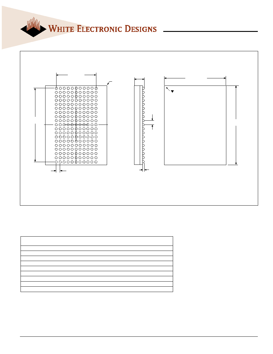
PACKAGE DIMENSION: 209 BUMP PBGA
ALL LINEAR DIMENSIONS ARE IN MILLIMETERS AND PARENTHETICALLY IN INCHES
2.50 (0.099)
MAX
0.600 (0.024)
MAX
1.27 (0.050)
TYP
1.00 TYP
A
B
C
D
E
F
G
H
J
K
L
M
N
P
R
T
U
V
W
14.00 (0.551) TYP
A1
CORNER
18.00
TYP
22.00 (0.866)
TYP
10.00 (0.394)
TYP
R 1.52 (0.060)
MAX (4x)
11 10
9
8
7
6
5
4
3
2
1
ORDERING INFORMATION
Commercial Temp Range (0�C to 70�C), Industrial Temp. Range (-40� to 85�C)
Part Number
Configuration
t
CD
Clock
Operating
(ns)
(MHz)
Range
W2Z1M72SJ35ES
1M x 72
3.5
166
Engineering Samples
W2Z1M72SJ38ES
1M x 72
3.8
150
Engineering Samples
W2Z1M72SJ28BC
1M x 72
2.8
225
Commercial
W2Z1M72SJ30BC
1M x 72
3.0
200
Commercial
W2Z1M72SJ35BC
1M x 72
3.5
166
Commercial
W2Z1M72SJ38BC
1M x 72
3.8
150
Commercial
W2Z1M72SJ30BI
1M x 72
3.0
200
Industrial
W2Z1M72SJ35BI
1M x 72
3.5
166
Industrial
W2Z1M72SJ38BI
1M x 72
3.8
150
Industrial
NOTE: Ball attach pad for above BGA package is 620 microns in diameter. Pad is solder mask defined.