1
White Electronic Designs Corporation ∑ (602) 437-1520 ∑ www.wedc.com
White Electronic Designs
January 2005
Rev. 1
W364M72V-XSBX
ADVANCED*
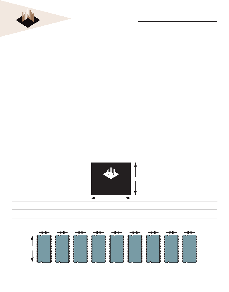
Discrete Approach
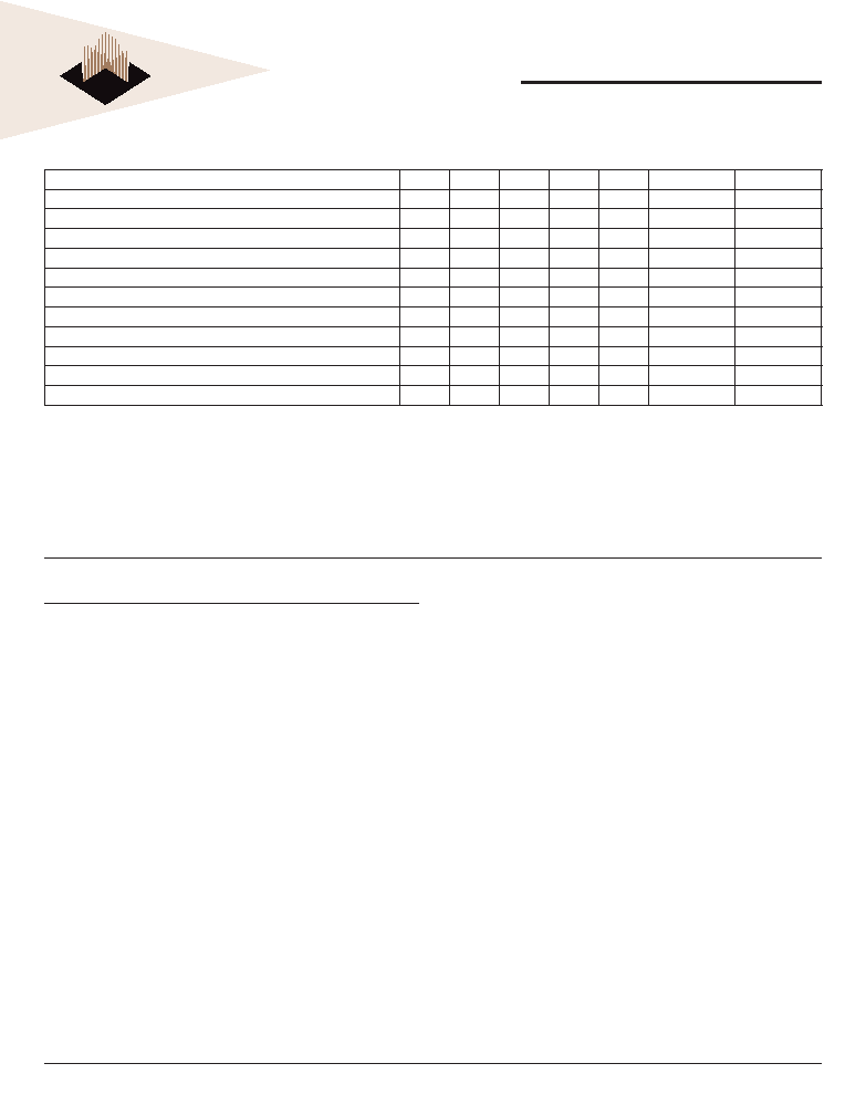
SAVINGS ≠ Area: 66% ≠ I/O Count: 55%
Area = 800mm
2
Area: 9 x 265mm
2
= 2,385mm
2
I/O Count = 219 Balls
I/O Count: 9 x 54 pins = 486 pins
11.9
11.9
11.9
11.9
11.9
11.9
11.9
11.9
11.9
22.3
54
TSOP
54
TSOP
54
TSOP
54
TSOP
54
TSOP
54
TSOP
54
TSOP
54
TSOP
54
TSOP
ACTUAL SIZE
25
32
White Electronic Designs
W364M72V-XSBX
BENEFITS
66% SPACE SAVINGS
Reduced part count from 9 to 1
Reduced I/O count
∑ 55% I/O Reduction
Reduced trace lengths for lower parasitic
capacitance
Suitable for hi-reliability applications
Laminate interposer for optimum TCE match
GENERAL DESCRIPTION
The 512MByte (4.5Gb) SDRAM is a high-speed CMOS,
dynamic random-access, memory using 9 chips containing
512M bits. Each chip is internally confi gured as a quad-
bank DRAM with a synchronous interface. Each of the
chip's 134,217,728-bit banks is organized as 8,192 rows
by 2,048 columns by 8 bits.
Read and write accesses to the SDRAM are burst oriented;
accesses start at a selected location and continue for a
64Mx72 Synchronous DRAM
FEATURES
High Frequency = 100, 125MHz
Package:
∑ 219 Plastic Ball Grid Array (PBGA), 32 x 25mm
3.3V ±0.3V power supply for core and I/Os
Fully Synchronous; all signals registered on positive
edge of system clock cycle
Internal pipelined operation; column address can be
changed every clock cycle
Internal banks for hiding row access/precharge
Programmable Burst length 1,2,4,8 or full page
8,192 refresh cycles
Commercial, Industrial and Military Temperature
Ranges
Organized as 64M x 72
Weight: W364M72V-XSBX - TBD grams typical
* This product is under development, is not qualifi ed or characterized and is subject to
change or cancellation without notice.

2
White Electronic Designs Corporation ∑ (602) 437-1520 ∑ www.wedc.com
White Electronic Designs
January 2005
Rev. 1
W364M72V-XSBX
ADVANCED
programmed number of locations in a programmed
sequence. Accesses begin with the registration of an
ACTIVE command, which is then followed by a READ or
WRITE command. The address bits registered coincident
with the ACTIVE command are used to select the bank
and row to be accessed (BA0, BA1 select the bank; A0-12
select the row). The address bits registered coincident
with the READ or WRITE command are used to select
the starting column location for the burst access.
The SDRAM provides for programmable READ or WRITE
burst lengths of 1, 2, 4 or 8 locations, or the full page, with
a burst terminate option. An AUTO PRECHARGE function
may be enabled to provide a self-timed row precharge that
is initiated at the end of the burst sequence.
The 4.5Gb SDRAM uses an internal pipelined architecture to
achieve high-speed operation. This architecture is compatible
with the 2n rule of prefetch architectures, but it also allows
the column address to be changed on every clock cycle to
achieve a high-speed, fully random access. Precharging one
bank while accessing one of the other three banks will hide
the precharge cycles and provide seamless, high-speed,
random-access operation.
The 4.5Gb SDRAM is designed to operate at 3.3V. An
auto refresh mode is provided, along with a power-saving,
power-down mode.
3
White Electronic Designs Corporation ∑ (602) 437-1520 ∑ www.wedc.com
White Electronic Designs
January 2005
Rev. 1
W364M72V-XSBX
ADVANCED
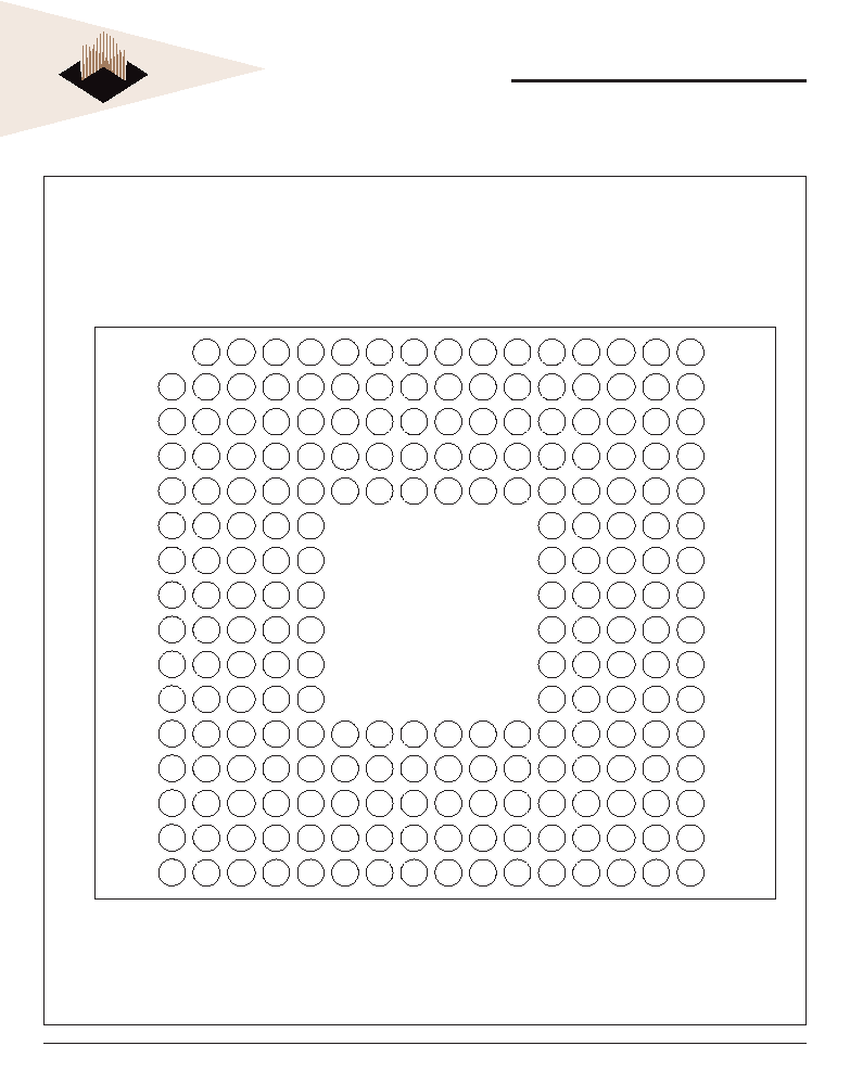
FIGURE 1 ≠ PIN CONFIGURATION
NOTE: DNU = Do Not Use; to be left unconnected for future upgrades.
NC = Not Connected Internally.
Top View
1
2
3
4
5
6
7
8
9
10
11
12
13
14
15
16
A
B
C
D
E
F
G
H
J
K
L
M
N
P
R
T
DQ
1
DQ
3
DQ
6
DQ
7
CAS
0
#
CS
0
#
V
SS
V
SS
NC
NC
DQ
56
DQ
57
DQ
60
DQ
62
Vss
V
SS
DQ
30
DQ
28
DQ
25
DQ
24
CLK
1
CKE
1
V
CC
V
CC
CS
2
#
CAS
2
#
DQ
39
DQ
38
DQ
35
DQ
33
V
CC
DQ
0
DQ
2
DQ
4
DQ
5
DQML0
WE
0
#
RAS
0
#
V
SS
V
SS
CKE
3
CLK
3
DQMH3
DQ
58
DQ
59
DQ
61
DQ
63
DQ
31
DQ
29
DQ
27
DQ
26
NC
DQMH1
NC
V
CCQ
V
CCQ
RAS
2
#
WE
2
#
DQML2
DQ
37
DQ
36
DQ
34
DQ
32
DQ
14
DQ
12
DQ
10
DQ
8
V
CC
V
CC
V
CC
V
CC
V
CC
V
CC
V
CC
V
CC
DQ
55
DQ
53
DQ
51
DQ
49
DQ
17
DQ
19
DQ
21
DQ
23
V
SS
V
SS
V
SS
Vss
V
SS
V
SS
V
SS
V
SS
DQ
40
DQ
42
DQ
44
DQ
46
DQ
15
DQ
13
DQ
11
DQ
9
DQMH0
CLK
0
CKE
0
V
CCQ
V
CCQ
CS
3
#
CAS
3
#
WE
3
#
DQ
54
DQ
52
DQ
50
DQ
48
DQ
16
DQ
18
DQ
20
DQ
22
DQML1
WE
1
#
CS
1
#
V
SS
V
SS
CKE
2
CLK
2
DQMH2
DQ
41
DQ
43
DQ
45
DQ
47
V
SS
V
SS
V
CC
V
CCQ
NC
NC
NC
V
SS
V
SS
NC
RAS
3
#
DQML3
NC
V
SS
V
CC
V
CCQ
V
CCQ
V
CC
V
SS
V
SS
NC
RAS
1
#
CAS
1
#
V
CC
V
CC
NC
NC
CS
4
#
NC
V
CC
V
SS
V
SS
A
9
A
0
A
2
A
12
NC
NC
NC
NC
NC
NC
A
8
A
1
A
3
DNU
NC
WE
4
#
DQ
70
DQ
68
DQ
66
DQ
64
A
10
A
7
A
5
DNU
BA
0
CLK
4
NC
NC
NC
NC
A
11
A
6
A
4
DNU
BA
1
CAS
4
#
DQ
71
DQ
69
DQ
67
DQ
65
V
SS
V
SS
V
CC
V
CCQ
NC
CKE
4
NC
V
SS
V
CC
V
CCQ
V
CCQ
V
CC
V
SS
V
SS
NC
RAS
4
#
DQML4
V
CC
V
SS
V
SS

4
White Electronic Designs Corporation ∑ (602) 437-1520 ∑ www.wedc.com
White Electronic Designs
January 2005
Rev. 1
W364M72V-XSBX
ADVANCED
FIGURE 2 ≠ FUNCTIONAL BLOCK DIAGRAM
A
0-12
A
0-12
BA
0-1
BA
0-1
CLK
0
CLK
DQ
0
DQ
7
CKE
0
CKE
DQML
0
DQML
DQ
0
DQ
7
IC1
A
0-12
BA
0-1
CLK
1
CLK
DQ
16
DQ
23
DQ
0
DQ
7
IC0
CKE
1
CKE
DQML
1
DQM
DQ
0
DQ
7
IC2
A
0-12
BA
0-1
CLK
2
CLK
DQ
32
DQ
39
CKE
2
CKE
DQML
2
DQM
DQ
0
DQ
7
IC3
A
0-12
BA
0-1
CLK
3
CLK
DQ
48
DQ
55
CKE
3
CKE
DQML
3
DQM
DQ
0
DQ
7
IC4
A
0-12
BA
0-1
CLK
4
CLK
DQ
64
DQ
71
CKE
4
CKE
DQML
4
DQM
CS
0
#
CLK
0
CKE
0
DQMH
0
CS
0
#
CS#
RAS
0
#
WE
0
#
CAS
0
#
WE# RAS# CAS#
CS
1
#
CS#
CLK
1
CLK
CKE
1
CKE
DQMH
1
DQM
CS
1
#
CS#
RAS
1
#
WE
1
#
CAS
1
#
WE# RAS# CAS#
CS
2
#
CS#
CLK
2
CLK
CKE
2
CKE
DQMH
2
DQM
CS
2
#
CS#
RAS
2
#
WE
2
#
CAS
2
#
WE# RAS# CAS#
CS
3
#
CS#
CLK
3
CLK
CKE
3
CKE
DQMH
3
DQM
CS
3
#
CS#
RAS
3
#
WE
3
#
CAS
3
#
WE# RAS# CAS#
CS
4
#
CS#
RAS
4
#
WE
4
#
CAS
4
#
WE# RAS# CAS#
A
0-12
BA
0-1
CLK
DQ
8
DQ
15
CKE
DQM
DQ
0
DQ
7
IC6
A
0-12
BA
0-1
DQ
24
DQ
31
DQ
0
DQ
7
IC5
DQ
0
DQ
7
IC7
A
0-12
BA
0-1
DQ
40
DQ
47
DQ
0
DQ
7
IC8
A
0-12
BA
0-1
DQ
56
DQ
63
CS#
WE# RAS# CAS#
WE# RAS# CAS#
WE# RAS# CAS#
WE# RAS# CAS#

5
White Electronic Designs Corporation ∑ (602) 437-1520 ∑ www.wedc.com
White Electronic Designs
January 2005
Rev. 1
W364M72V-XSBX
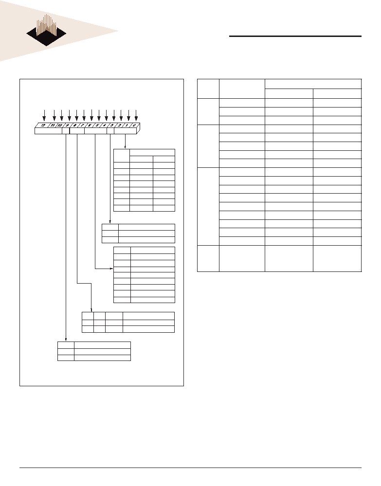
REGISTER DEFINITION
MODE REGISTER
The Mode Register is used to defi ne the specifi c mode
of op er a tion of the SDRAM. This defi nition includes the
selec-tion of a burst length, a burst type, a CAS latency,
an op er at ing mode and a write burst mode, as shown in
Figure 3. The Mode Register is programmed via the LOAD
MODE REG IS TER command and will retain the stored
in for ma tion until it is programmed again or the device
loses power.
Mode register bits M0-M2 specify the burst length, M3
spec i fi es the type of burst (sequential or in ter leaved),
M4-M6 specify the CAS latency, M7 and M8 specify the
op er at ing mode, M9 spec i fi es the WRITE burst mode,
and M10 and M11 are reserved for future use. Address
A12 (M12) is undefi ned but should be driven LOW during
loading of the mode register.
The Mode Register must be loaded when all banks are
idle, and the controller must wait the specifi ed time before
ini ti at ing the subsequent operation. Violating either of these
requirements will result in unspecifi ed operation.
BURST LENGTH
Read and write accesses to the SDRAM are burst oriented,
with the burst length being programmable, as shown
in Fig ure 3. The burst length determines the maximum
number of column lo ca tions that can be accessed for a
given READ or WRITE command. Burst lengths of 1, 2, 4
or 8 locations are avail able for both the sequential and the
interleaved burst types, and a full-page burst is available
for the sequential type. The full-page burst is used in
conjunction with the BURST TERMINATE command to
generate arbitrary burst lengths.
Reserved states should not be used, as unknown op er a tion
or incompatibility with future versions may result.
When a READ or WRITE command is issued, a block of
col umns equal to the burst length is effectively selected.
All accesses for that burst take place within this block,
mean ing that the burst will wrap within the block if a
boundary is reached. The block is uniquely selected by
A1-9, A11 when the burst length is set to two; by A2-9,
A11 when the burst length is set to four; and by A3-9, A11
when the burst length is set to eight. The remaining (least
signifi cant) address bit(s) is (are) used to select the starting
location within the block. Full-page bursts wrap within the
page if the boundary is reached.
All inputs and outputs are LVTTL compatible. SDRAMs offer
sub stan tial ad vanc es in DRAM op er at ing per for mance,
in clud ing the ability to syn chro nous ly burst data at a high
data rate with au to mat ic column-ad dress gen er a tion,
the ability to in ter leave be tween in ter nal banks in order
to hide precharge time and the capability to ran dom ly
change col umn ad dress es on each clock cy cle dur ing a
burst ac cess.
FUNCTIONAL DE SCRIP TION
Read and write accesses to the SDRAM are burst oriented;
accesses start at a selected location and continue for
a pro grammed number of locations in a pro grammed
se quence. Ac cess es begin with the registration of an
ACTIVE com mand which is then followed by a READ or
WRITE com mand. The address bits registered coincident
with the AC TIVE command are used to select the bank and
row to be accessed (BA0 and BA1 select the bank, A0-12
select the row). The address bits (A0-9, A11) reg is tered
coincident with the READ or WRITE com mand are used to
select the start ing column location for the burst access.
Prior to normal operation, the SDRAM must be initialized.
The following sections provide detailed information
cov er ing device initialization, register defi nition, command
de scrip tions and de vice operation.
INITIALIZATION
SDRAMs must be pow ered up and initialized in a pre defi ned
manner. Operational pro ce dures other than those spec i fi ed
may result in undefi ned operation. Once power is ap plied
to V
CC
and V
CCQ
(si mul ta neous ly) and the clock is stable
(stable clock is de fi ned as a signal cycling within tim ing
constraints specified for the clock pin), the SDRAM
re quires a 100µs delay prior to issuing any command
other than a COMMAND INHIBIT or a NOP. Starting at
some point during this 100µs period and continuing at
least through the end of this period, COMMAND INHIBIT
or NOP com mands should be applied.
Once the 100µs delay has been satisfi ed with at least
one COM MAND INHIBIT or NOP command having been
ap plied, a PRECHARGE command should be applied. All
banks must be precharged, thereby placing the device in
the all banks idle state.
Once in the idle state, two AUTO REFRESH cycles must be
per formed. After the AUTO REFRESH cycles are complete,
the SDRAM is ready for Mode Register programming.
Be cause the Mode Register will power up in an unknown
state, it should be loaded prior to applying any operational
command.
ADVANCED
6
White Electronic Designs Corporation ∑ (602) 437-1520 ∑ www.wedc.com
White Electronic Designs
January 2005
Rev. 1
W364M72V-XSBX
TABLE 1 ≠ BURST DEFINITION
Burst
Length
Starting Column
Address
Order of Accesses Within a Burst
Type = Sequential
Type = In ter leaved
2
A0
0
0-1
0-1
1
1-0
1-0
4
A1
A0
0
0
0-1-2-3
0-1-2-3
0
1
1-2-3-0
1-0-3-2
1
0
2-3-0-1
2-3-0-1
1
1
3-0-1-2
3-2-1-0
8
A2
A1
A0
0
0
0
0-1-2-3-4-5-6-7
0-1-2-3-4-5-6-7
0
0
1
1-2-3-4-5-6-7-0
1-0-3-2-5-4-7-6
0
1
0
2-3-4-5-6-7-0-1
2-3-0-1-6-7-4-5
0
1
1
3-4-5-6-7-0-1-2
3-2-1-0-7-6-5-4
1
0
0
4-5-6-7-0-1-2-3
4-5-6-7-0-1-2-3
1
0
1
5-6-7-0-1-2-3-4
5-4-7-6-1-0-3-2
1
1
0
6-7-0-1-2-3-4-5
6-7-4-5-2-3-0-1
1
1
1
7-0-1-2-3-4-5-6
7-6-5-4-3-2-1-0
Full
Page
(y)
n = A
0
-9
(location 0-y)
Cn, Cn + 1, Cn + 2
Cn + 3, Cn + 4...
...Cn - 1,
Cn...
Not Supported
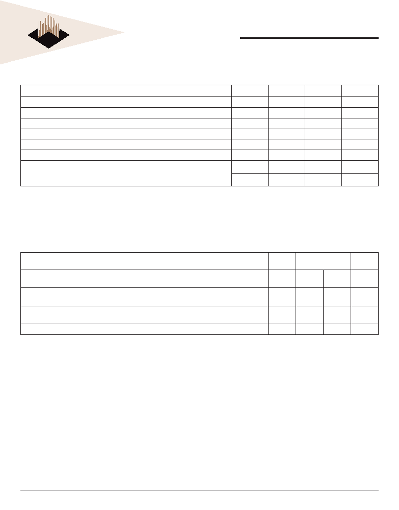
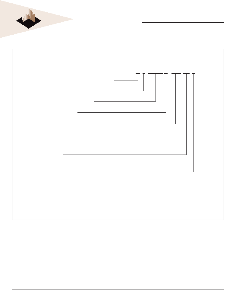
FIGURE 3 ≠ MODE REGISTER DEFINITION
NOTES:
1. For full-page accesses: y = 2,048.
2. For a burst length of two, A1-9, A11 select the block-of-two burst; A0 selects the
starting column within the block.
3. For a burst length of four, A2-9, A11 select the block-of-four burst; A0-1 select the
starting column within the block.
4. For a burst length of eight, A3-9, A11 select the block-of-eight burst; A0-2 select the
starting column within the block.
5. For a full-page burst, the full row is selected and A0-9, A11 select the starting
column.
6. Whenever a boundary of the block is reached within a given sequence above, the
following access wraps within the block.
7. For a burst length of one, A0-9, A11 select the unique column to be accessed, and
Mode Register bit M3 is ignored.
M3 = 0
1
2
4
8
Reserved
Reserved
Reserved
Full Page
M3 = 1
1
2
4
8
Reserved
Reserved
Reserved
Reserved
Operating Mode
Standard Operation
All other states reserved
0
-
0
-
Defined
-
0
1
Burst Type
Sequential
Interleaved
CAS Latency
Reserved
Reserved
2
3
Reserved
Reserved
Reserved
Reserved
Burst Length
M0
0
1
0
1
0
1
0
1
Burst Length
CAS Latency
BT
A
9
A
7
A
6
A
5
A
4
A
3
A
8
A
2
A
1
A
0
Mode Register (Mx)
Address Bus
M1
0
0
1
1
0
0
1
1
M2
0
0
0
0
1
1
1
1
M3
M4
0
1
0
1
0
1
0
1
M5
0
0
1
1
0
0
1
1
M6
0
0
0
0
1
1
1
1
M6-M0
M8
M7
Op Mode
A
10
A
11
Reserved*
WB
0
1
Write Burst Mode
Programmed Burst Length
Single Location Access
M9
*Should program
M12, M11, M10 = 0, 0
to ensure compatibility
with future devices.
A
12
ADVANCED
7
White Electronic Designs Corporation ∑ (602) 437-1520 ∑ www.wedc.com
White Electronic Designs
January 2005
Rev. 1
W364M72V-XSBX
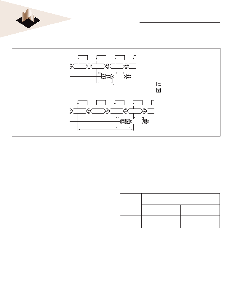
FIGURE 4 ≠ CAS LATENCY
OPERATING MODE
The nor mal operating mode is selected by setting M7and
M8 to zero; the other combinations of values for M7 and
M8 are re served for future use and/or test modes. The
pro grammed burst length applies to both READ and
WRITE bursts.
Test modes and reserved states should not be used
be cause unknown operation or incompatibility with future
versions may result.
TABLE 2 ≠ CAS LATENCY
SPEED
ALLOWABLE OPERATING
FREQUENCY (MHz)
CAS
LATENCY = 2
CAS
LATENCY = 3
-100
75
100
-125
100
125
WRITE BURST MODE
When M9 = 0, the burst length programmed via M0-M2
applies to both READ and WRITE bursts; when M9 = 1,
the programmed burst length applies to READ bursts, but
write accesses are single-location (nonburst) accesses.
CLK
Command
I/O
CLK
Command
I/O
T0 T1 T2 T3
T0 T1 T2 T3 T4
READ NOP NOP
CAS Latency = 2
D
OUT
t
LZ
t
OH
t
AC
READ NOP NOP NOP
D
OUT
t
LZ
t
OH
t
AC
CAS Latency = 3
DON'T CARE
UNDEFINED
BURST TYPE
Accesses within a given burst may be pro grammed to be
either se quen tial or interleaved; this is re ferred to as the
burst type and is selected via bit M3.
The ordering of accesses within a burst is de ter mined by
the burst length, the burst type and the start ing column
address, as shown in Table 1.
CAS LATENCY
The CAS latency is the delay, in clock cycles, between
the registration of a READ command and the avail abil i ty
of the fi rst piece of output data. The latency can be set to
two or three clocks.
If a READ command is registered at clock edge n, and the
latency is m clocks, the data will be available by clock edge
n+m. The I/Os will start driving as a result of the clock
edge one cycle ear li er (n + m - 1), and provided that the
rel e vant access times are met, the data will be valid by
clock edge n + m. For example, assuming that the clock
cycle time is such that all relevant access times are met,
if a READ command is registered at T0 and the latency
is pro grammed to two clocks, the I/Os will start driving
after T1 and the data will be valid by T2. Table 2 below
indicates the op er at ing fre quen cies at which each CAS
latency setting can be used.
Reserved states should not be used as unknown op er a tion
or incompatibility with future versions may result.
ADVANCED
8
White Electronic Designs Corporation ∑ (602) 437-1520 ∑ www.wedc.com
White Electronic Designs
January 2005
Rev. 1
W364M72V-XSBX
TRUTH TABLE - COMMANDS AND DQM OPERATION (NOTE 1)
NAME (FUNCTION)
CS#
RAS#
CAS#
WE#
DQM
ADDR
I/Os
COMMAND
INHIBIT
(NOP)
H X X X X
X
X
NO OPERATION (NOP)
L
H
H
H
X
X
X
ACTIVE (Select bank and activate row) ( 3)
L
L
H
H
X
Bank/Row
X
READ (Select bank and column, and start READ burst) (4)
L
H
L
H
L/H
8
Bank/Col
X
WRITE (Select bank and column, and start WRITE burst) (4)
L
H
L
L
L/H
8
Bank/Col
Valid
BURST
TERMINATE
L H H L X
X
Active
PRECHARGE (Deactivate row in bank or banks) ( 5)
L
L
H
L
X
Code
X
AUTO REFRESH or SELF REFRESH (Enter self refresh mode) (6, 7)
L
L
L
H
X
X
X
LOAD MODE REGISTER (2)
L
L
L
L
X
Op-Code
X
Write Enable/Output Enable (8)
≠
≠
≠
≠
L
≠
Active
Write Inhibit/Output High-Z (8)
≠
≠
≠
≠
H
≠
High-Z
command can only be issued when all banks are idle, and
a sub se quent ex e cut able com mand cannot be issued until
t
MRD
is met.
ACTIVE
The ACTIVE command is used to open (or activate) a
row in a particular bank for a subsequent access. The
value on the BA0, BA1 inputs se lects the bank, and the
address pro vid ed on inputs A0-12 selects the row. This row
remains active (or open) for ac cess es until a PRECHARGE
com mand is issued to that bank. A PRECHARGE
command must be issued before opening a different row
in the same bank.
READ
The READ command is used to initiate a burst read access
to an active row. The value on the BA0, BA1 inputs selects
the bank, and the address provided on inputs A0-9, A11
se lects the starting column location. The value on input
A10 de ter mines whether or not AUTO PRECHARGE is
used. If AUTO PRECHARGE is selected, the row being
accessed will be precharged at the end of the READ
burst; if AUTO PRECHARGE is not selected, the row will
remain open for subsequent ac cess es. Read data appears
on the I/Os sub ject to the logic level on the DQM inputs
COMMANDS
The Truth Table provides a quick reference of available
com mands. This is followed by a written de scrip tion of each
com mand. Three additional Truth Tables appear following
the Op er a tion section; these tables provide current state/
next state information.
COMMAND INHIBIT
The COMMAND INHIBIT function pre vents new commands
from being executed by the SDRAM, regardless of whether
the CLK signal is enabled. The SDRAM is effectively
de se lect ed. Op er a tions already in progress are not
affected.
NO OPERATION (NOP)
The NO OPERATION (NOP) command is used to perform
a NOP to an SDRAM which is selected (CS# is LOW).
This pre vents unwanted commands from being registered
dur ing idle or wait states. Op er a tions already in progress
are not affected.
LOAD MODE REGISTER
The Mode Register is loaded via inputs A0-11 (A12
should be driven low). See Mode Reg is ter heading in the
Register Defi ni tion sec tion. The LOAD MODE REGISTER
NOTES:
1. CKE is HIGH for all commands shown except SELF REFRESH.
2. A0-11 defi ne the op-code written to the Mode Register and A12 should be driven
low.
3. A0-12 provide row address, and BA0, BA1 determine which bank is made active.
4. A0-9, A11 provide column address; A10 HIGH enables the auto precharge feature
(nonpersistent), while A10 LOW disables the auto precharge feature; BA0, BA1
determine which bank is being read from or written to.
5. A10 LOW: BA0, BA1 determine the bank being precharged. A10 HIGH: All banks
precharged and BA0, BA1 are "Don't Care."
6. This command is AUTO REFRESH if CKE is HIGH; SELF REFRESH if CKE is
LOW.
7. Internal refresh counter controls row addressing; all inputs and I/Os are "Don't
Care" except for CKE.
8. Activates or deactivates the I/Os during WRITEs (zero-clock delay) and READs
(two-clock delay).
ADVANCED

9
White Electronic Designs Corporation ∑ (602) 437-1520 ∑ www.wedc.com
White Electronic Designs
January 2005
Rev. 1
W364M72V-XSBX
two clocks earlier. If a given DQM signal was registered
HIGH, the cor re spond ing I/Os will be High-Z two clocks
later; if the DQM signal was registered LOW, the I/Os will
provide valid data.
WRITE
The WRITE command is used to initiate a burst write
access to an active row. The value on the BA0, BA1
inputs selects the bank, and the address provided on
inputs A0-9, A11 se lects the starting column location.
The value on input A10 de ter mines whether or not AUTO
PRECHARGE is used. If AUTO PRECHARGE is selected,
the row being accessed will be precharged at the end of
the WRITE burst; if AUTO PRECHARGE is not selected,
the row will remain open for sub se quent accesses. Input
data appearing on the I/Os is written to the memory array
subject to the DQM input logic level ap pear ing co in ci dent
with the data. If a given DQM signal is registered LOW,
the cor re spond ing data will be written to memory; if the
DQM signal is registered HIGH, the cor re spond ing data
inputs will be ignored, and a WRITE will not be executed
to that byte/column location.
PRECHARGE
The PRECHARGE command is used to deactivate the
open row in a particular bank or the open row in all banks.
The bank(s) will be available for a subsequent row access
a specifi ed time (tRP) after the PRECHARGE command
is is sued. Input A10 determines wheth er one or all banks
are to be precharged, and in the case where only one
bank is to be precharged, inputs BA0, BA1 select the bank.
Oth er wise BA0, BA1 are treated as "Don't Care." Once a
bank has been precharged, it is in the idle state and must
be activated pri or to any READ or WRITE commands being
is sued to that bank.
AUTO PRECHARGE
AUTO PRECHARGE is a feature which performs the same
in di vid u al-bank PRECHARGE function de scribed above,
with out re quir ing an explicit command. This is ac com plished
by using A10 to enable AUTO PRECHARGE in conjunction
with a spe cifi c READ or WRITE command. A precharge of
the bank/row that is ad dressed with the READ or WRITE
com mand is au to mat i cal ly performed upon com ple tion of
the READ or WRITE burst, except in the full-page burst
mode, where AUTO PRECHARGE does not ap ply. AUTO
PRECHARGE is non per sis tent in that it is either enabled or
disabled for each in di vid u al READ or WRITE com mand.
AUTO PRECHARGE ensures that the precharge is initiated
at the earliest valid stage within a burst. The user must not
is sue another command to the same bank until the precharge
time (t
RP
) is completed. This is determined as if an explicit
PRECHARGE com mand was issued at the earliest possible
time.
BURST TERMINATE
The BURST TERMINATE command is used to truncate
either fi xed-length or full-page bursts. The most recently
reg is tered READ or WRITE command prior to the BURST
TER MI NATE command will be truncated.
AUTO REFRESH
AUTO REFRESH is used during normal op er a tion of
the SDRAM and is analagous to CAS#-BEFORE-RAS#
(CBR) RE FRESH in con ven tion al DRAMs. This com mand
is nonpersistent, so it must be issued each time a refresh
is required.
The addressing is generated by the internal refresh
con trol ler. This makes the address bits "Don't Care" during
an AUTO RE FRESH command. Each 512Mb SDRAM
requires 8,192 AUTO RE FRESH cycles every refresh
period (t
REF
). Pro vid ing a dis trib ut ed AUTO RE FRESH
command will meet the refresh re quire ment and ensure
that each row is re freshed. Al ter na tive ly, 8,192 AUTO
RE FRESH com mands can be is sued in a burst at the
minimum cycle rate (t
RC
), once every refresh period
(t
REF
).
SELF REFRESH*
The SELF REFRESH command can be used to retain data
in the SDRAM, even if the rest of the system is powered
down. When in the self refresh mode, the SDRAM retains
data with out external clocking. The SELF RE FRESH
command is ini ti at ed like an AUTO REFRESH com mand
except CKE is dis abled (LOW). Once the SELF RE FRESH
command is reg is tered, all the inputs to the SDRAM
become "Don't Care," with the exception of CKE, which
must remain LOW.
Once self refresh mode is engaged, the SDRAM provides
its own internal clocking, causing it to perform its own
AUTO REFRESH cycles. The SDRAM must remain in
self refresh mode for a minimum period equal to tRAS and
may remain in self refresh mode for an indefi nite period
beyond that.
The procedure for exiting self refresh requires a sequence
of commands. First, CLK must be stable (stable clock
is defi ned as a signal cycling within timing con straints
* Self refresh available in commercial and industrial tem per a tures only.
ADVANCED
10
White Electronic Designs Corporation ∑ (602) 437-1520 ∑ www.wedc.com
White Electronic Designs
January 2005
Rev. 1
W364M72V-XSBX
ABSOLUTE MAXIMUM RATINGS
Parameter
Unit
Voltage on V
CC
, V
CCQ
Supply relative to Vss
-1 to 4.6
V
Voltage on NC or I/O pins relative to Vss
-1 to 4.6
V
Operating Temperature TA (Mil)
-55 to +125
∞C
Operating Temperature TA (Ind)
-40 to +85
∞C
Storage Temperature, Plastic
-55 to +125
∞C
NOTE:
Stress greater than those listed under "Absolute Maximum Ratings" may cause per ma nent damage to the device. This is a stress rating only and
func tion al op er a tion of the device at these or any other conditions greater than those in di cat ed in the operational sections of this specifi cation is not
implied. Exposure to ab so lute maximum rating con di tions for extended periods may affect reliability.
CAPACITANCE (NOTE 2)
Parameter
Symbol
Max
Unit
Input Capacitance: CLK
CI1
TBD
pF
Addresses, BA0-1 Input Capacitance
CA
TBD
pF
Input Capacitance: All other input-only pins
CI2
TBD
pF
Input/Output Capacitance: I/Os
CIO
TBD
pF
BGA THERMAL RESISTANCE
Description
Symbol
Max
Unit
Junction to Ambient (No Airfl ow)
Theta JA
TBD
C/W
Junction to Ball
Theta JB
TBD
C/W
Junction to Case (Top)
Theta JC
TBD
C/W
NOTE:
Refer to Application Note "PBGA Thermal Resistance Correlation" at www.wedc.com in the application notes section for modeling conditions.
spec i fied for the clock pin) prior to CKE going back
HIGH. Once CKE is HIGH, the SDRAM must have NOP
commands is sued (a minimum of two clocks) for t
XSR
,
because time is required for the com ple tion of any internal
refresh in progress.
Upon exiting the self refresh mode, AUTO REFRESH
com mands must be issued as both SELF REFRESH and
AUTO REFRESH utilize the row refresh counter.
ADVANCED
11
White Electronic Designs Corporation ∑ (602) 437-1520 ∑ www.wedc.com
White Electronic Designs
January 2005
Rev. 1
W364M72V-XSBX
DC ELECTRICAL CHARACTERISTICS AND OPERATING CONDITIONS (NOTES 1, 6)
V
CC
, V
CCQ
= +3.3V ± 0.3V; -55∞C T
A
+125∞C
Parameter/Condition
Symbol
Min
Max
Units
Supply Voltage
V
CC
,V
CCQ
3
3.6
V
Input High Voltage: Logic 1; All inputs (21)
V
IH
2 V
CC
+ 0.3
V
Input Low Voltage: Logic 0; All inputs (21)
V
IL
-0.3 0.8 V
Input Leakage Current: Any input 0V V
IN
V
CC
(All other pins not under test = 0V)
I
I
10
10
µA
Input Leakage Address Current (All other pins not under test = 0V)
I
I
-45
45
µA
Output Leakage Current: I/Os are disabled; 0V
V
OUT
V
CCQ
I
OZ
-5
5
µA
Output Levels:
Output High Voltage (I
OUT
= -4mA)
Output Low Voltage (I
OUT
= 4mA)
V
OH
2.4 ≠ V
V
OL
≠ 0.4 V
ICC SPECIFICATIONS AND CONDITIONS (NOTES 1,6,11,13)
V
CC
, V
CCQ
= +3.3V ± 0.3V; -55∞C T
A
+125∞C
Parameter/Condition
Symbol
Max
Units
-125
-100
Operating Current: Active Mode;
Burst = 2; Read or Write; t
RC
= t
RC
(min); CAS latency = 3 (3, 18, 19)
I
CC1
990
900
mA
Standby Current: Active Mode; CKE = HIGH; CS# = HIGH;
All banks active after t
RCD
met; No accesses in progress (3, 12, 19)
I
CC3
405
405
mA
Operating Current: Burst Mode; Continuous burst;
Read or Write; All banks active; CAS latency = 3 (3, 18, 19)
I
CC4
1,035
990
mA
Self Refresh Current: CKE
0.2V (Commercial and Industrial Temperature: -40∞C to + 85∞C) (27)
I
CC7
54
54
mA
ADVANCED
12
White Electronic Designs Corporation ∑ (602) 437-1520 ∑ www.wedc.com
White Electronic Designs
January 2005
Rev. 1
W364M72V-XSBX
ELECTRICAL CHARACTERISTICS AND RECOMMENDED AC OPERATING CHARACTERISTICS
(NOTES 5, 6, 8, 9, 11)
Parameter
Symbol
-100
-125
Unit
Min
Max
Min
Max
Access time from CLK (pos. edge)
CL = 3
t
AC
7
6
ns
CL = 2
t
AC
7
6
ns
Address hold time
t
AH
1
1
ns
Address setup time
t
AS
2
2
ns
CLK high-level width
t
CH
3
3
ns
CLK low-level width
t
CL
3
3
ns
Clock cycle time (22)
CL = 3
t
CK
10
8
ns
CL = 2
t
CK
13
10
ns
CKE hold time
t
CKH
1
1
ns
CKE setup time
t
CKS
2
2
ns
CS#, RAS#, CAS#, WE#, DQM hold time
t
CMH
1
1
ns
CS#, RAS#, CAS#, WE#, DQM setup time
t
CMS
2
2
ns
Data-in hold time
t
DH
1
1
ns
Data-in setup time
t
DS
2
2
ns
Data-out high-impedance time
CL = 3 (10)
t
HZ
7
6
ns
CL = 2 (10)
t
HZ
7
6
ns
Data-out low-impedance time
t
LZ
1 1
ns
Data-out hold time (load) (26)
t
OH
3 3
ns
Data-out hold time (no load)
t
OHN
1.8
1.8
ns
ACTIVE to PRECHARGE command
t
RAS
50
120,000
50
120,000
ns
ACTIVE to ACTIVE command period
t
RC
70
68
ns
ACTIVE to READ or WRITE delay
t
RCD
20
20
ns
Refresh period (8,192 rows) ≠ Commercial, Industrial
t
REF
64
64
ms
Refresh period (8,192 rows) ≠ Military
t
REF
16
16
ms
AUTO REFRESH period
t
RFC
70 70
ns
PRECHARGE command period
t
RP
20
20 ns
ACTIVE bank A to ACTIVE bank B command
t
RRD
20
20
ns
Transition time (7)
t
T
0.3 1.2
0.3
1.2
ns
WRITE recovery time
(23)
t
WR
1 CLK + 7ns
1 CLK + 7ns
--
(24)
15 15
ns
Exit SELF REFRESH to ACTIVE command
t
XSR
80 80
ns
ADVANCED

13
White Electronic Designs Corporation ∑ (602) 437-1520 ∑ www.wedc.com
White Electronic Designs
January 2005
Rev. 1
W364M72V-XSBX
AC FUNCTIONAL CHARACTERISTICS (NOTES 5,6,7,8,9,11)
Parameter/Condition
Symbol
-100
-125
Units
READ/WRITE command to READ/WRITE command (17)
t
CCD
1
1
t
CK
CKE to clock disable or power-down entry mode (14)
t
CKED
1 1
t
CK
CKE to clock enable or power-down exit setup mode (14)
t
PED
1
1
t
CK
DQM to input data delay (17)
t
DQD
0 0
t
CK
DQM to data mask during WRITEs
t
DQM
0 0
t
CK
DQM to data high-impedance during READs
t
DQZ
2 2
t
CK
WRITE command to input data delay (17)
t
DWD
0 0
t
CK
Data-in to ACTIVE command (15)
t
DAL
4
5
t
CK
Data-in to PRECHARGE command (16)
t
DPL
2 2
t
CK
Last data-in to burst STOP command (17)
t
BDL
1
1
t
CK
Last data-in to new READ/WRITE command (17)
t
CDL
1 1
t
CK
Last data-in to PRECHARGE command (16)
t
RDL
2 2
t
CK
LOAD MODE REGISTER command to ACTIVE or REFRESH command (25)
t
MRD
2
2
t
CK
Data-out to high-impedance from PRECHARGE command (17)
CL = 3
t
ROH
3
3
t
CK
CL = 2
t
ROH
2
--
t
CK
NOTES:
1. All voltages referenced to V
SS
.
2. This parameter is not tested but guaranteed by design. f = 1 MHz, T
A
= 25∞C.
3. I
CC
is dependent on output loading and cycle rates. Specifi ed values are obtained
with minimum cycle time and the outputs open.
4. Enables on-chip refresh and address counters.
5. The minimum specifi cations are used only to indicate cycle time at which proper
operation over the full temperature range is ensured.
6. An initial pause of 100µs is required after power-up, followed by two AUTO
REFRESH commands, before proper device operation is ensured. (V
CC
and V
CCQ
must be powered up simultaneously.) The two AUTO REFRESH command wake-
ups should be repeated any time the t
REF
refresh re quire ment is exceeded.
7. AC characteristics assume t
T
= 1ns.
8. In addition to meeting the transition rate specifi cation, the clock and CKE must
transit between V
IH
and V
IL
(or between V
IL
and V
IH
) in a monotonic manner.
9. Outputs measured at 1.5V with equivalent load:
Q
50pF
10. t
HZ
defi nes the time at which the output achieves the open circuit condition; it is not
a reference to V
OH
or V
OL
. The last valid data element will meet t
OH
before going
High-Z.
11. AC timing and I
CC
tests have V
IL
= 0V and V
IH
= 3V, with timing referenced to 1.5V
crossover point.
12. Other input signals are allowed to transition no more than once every two clocks
and are otherwise at valid V
IH
or V
IL
levels.
13. I
CC
spec i fi ca tions are tested after the device is properly initialized.
14. Timing actually specifi ed by t
CKS
; clock(s) specifi ed as a reference only at minimum
cycle rate.
15. Timing actually specifi ed by t
WR
plus t
RP
; clock(s) specifi ed as a reference only at
minimum cycle rate.
16. Timing actually specifi ed by t
WR
.
17. Required clocks are specifi ed by JEDEC functionality and are not de pen dent on
any timing parameter.
18. The I
CC
current will decrease as the CAS latency is reduced. This is due to the fact
that the maximum cycle rate is slower as the CAS latency is reduced.
19. Address transitions average one transition every two clocks.
20. CLK must be toggled a minimum of two times during this period.
21. V
IH
overshoot: V
IH
(MAX) = V
CCQ
+ 2V for a pulse width 3ns, and the pulse width
cannot be greater than one third of the cycle rate. V
IL
undershoot: V
IL
(MIN) = -2V
for a pulse width
3ns.
22. The clock frequency must remain constant (stable clock is defi ned as a signal
cycling within timing constraints specifi ed for the clock pin) during access or
precharge states (READ, WRITE, including t
WR
, and PRECHARGE com mands).
CKE may be used to reduce the data rate.
23. Auto precharge mode only. The precharge timing budget (t
RP
) begins 7.5ns/7ns
after the fi rst clock delay, after the last WRITE is executed.
24. Precharge mode only.
25. JEDEC and PC100 specify three clocks.
26. Parameter guaranteed by design.
27. Self refresh available in commercial and industrial temperatures only.
ADVANCED
14
White Electronic Designs Corporation ∑ (602) 437-1520 ∑ www.wedc.com
White Electronic Designs
January 2005
Rev. 1
W364M72V-XSBX
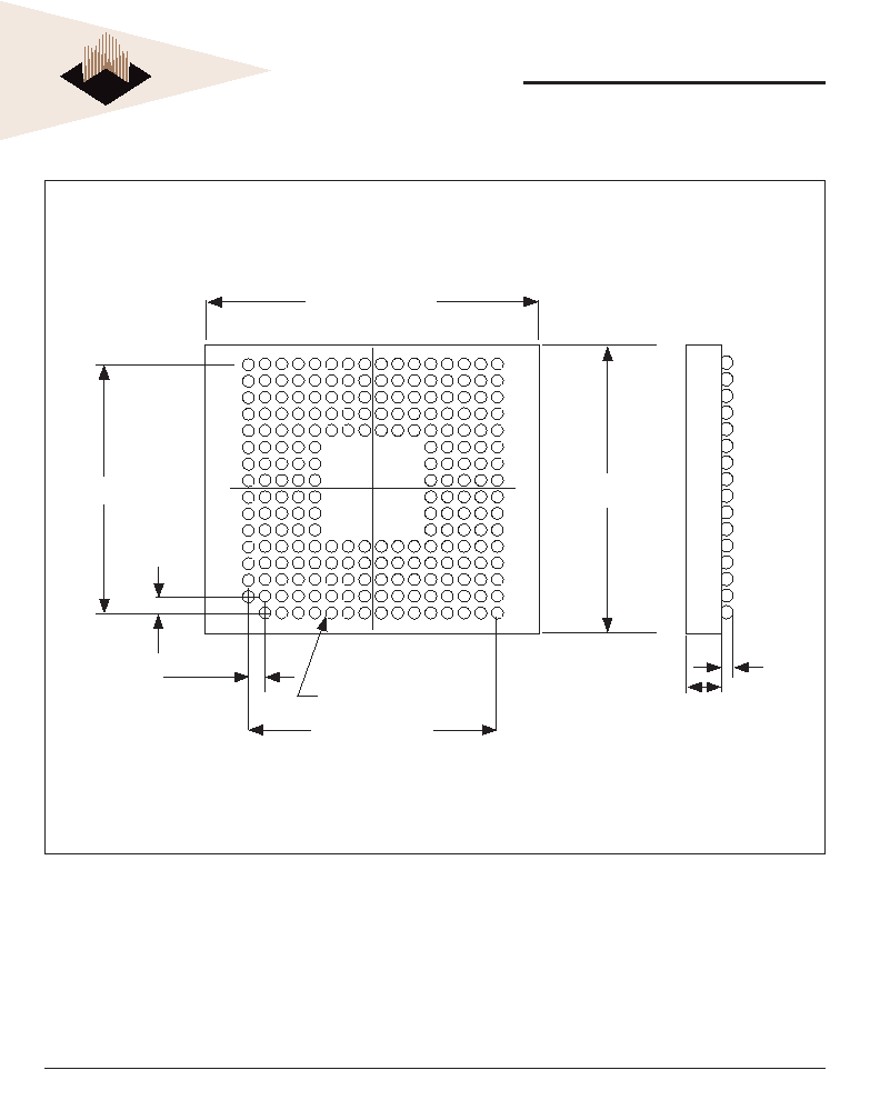
PACKAGE DIMENSION: 219 PLASTIC BALL GRID ARRAY (PBGA), 32mm x 25mm
ALL LINEAR DIMENSIONS ARE MILLIMETERS AND PARENTHETICALLY IN INCHES
Bottom View
32.1 (1.264) MAX
1 2 3 4 5 6 7 8 9 10 11
12
13
14
15
16
T
R
P
N
M
L
K
J
H
G
F
E
D
C
B
A
25.1 (0.988)
MAX
19.05 (0.750)
NOM
1.27 (0.050)
NOM
19.05 (0.750) NOM
2.96 (0.116)
MAX
0.61
(0.024)
NOM
219 x ÿ 0.762 (0.030) NOM
ADVANCED
15
White Electronic Designs Corporation ∑ (602) 437-1520 ∑ www.wedc.com
White Electronic Designs
January 2005
Rev. 1
W364M72V-XSBX
ORDERING INFORMATION
WHITE ELECTRONIC DESIGNS CORP.
SDRAM
CONFIGURATION, 64M x 72
3.3V Power Supply
FREQUENCY (MHz)
100 = 100MHz
125 = 125MHz
ES = Non-qualifi ed product
1
PACKAGE:
SB = 219 Plastic Ball Grid Array (PBGA), 32mm x 25mm
DEVICE GRADE:
M
= Mil
i tary
-55∞C to +125∞C
I = In
dus tri al -40∞C
to
+85∞C
C = Com
mer cial 0∞C
to
+70∞C
Blank = No temperature range specifi ed for 'ES' Non-qualifi ed product.
W 3 64M 72 V - XXX SB X
Note 1: W364M72V-ESSB is only available product until completion of qualifi cation.
ADVANCED

16
White Electronic Designs Corporation ∑ (602) 437-1520 ∑ www.wedc.com
White Electronic Designs
January 2005
Rev. 1
W364M72V-XSBX
Document Title
64M x 72 SDRAM Multi-Chip Package, 32mm x 25mm
Revision History
Rev #
History
Release Date
Status
Rev 0
Initial Release
May 2004
Advanced
Rev 1
Changes (Pg. 1, 5-15)
1.1 Added additional product data
January 2005
Advanced
ADVANCED