February 2002
Rev. 0
W3DG6430V-D2
1
White Electronic Designs
White Electronic Designs Corporation ∑ (602) 437-1520 ∑ www.wedc.com
PRELIMINARY*
256MB - 32M x 64 BUFFERED SDRAM MODULE
DESCRIPTION
The W3DG6430V is a 32M x 64 synchronous DRAM
module which consists of sixteen 32Mx4 SDRAM
components in TSOP II package, three very high speed
buffers for reduced input capacitance, and one 2K
EEPROM in an 8 pin TSSOP package for Serial Presence
Detect which are mounted on a 168 pin DIMM multilayer
FR4 Substrate.
* This product is not fully qualifi ed or characterized and is subject to change without
notice.
FEATURES
Burst
Mode
Operation
Auto and Self Refresh capability
LVTTL compatible inputs and outputs
Serial
Presence
Detect
with
EEPROM
Fully synchronous: All signals are registered on the positive
edge of the system clock
Programmable Burst Lengths: 1, 2, 4, 8 or Full Page
3.3V ± 0.3V Power Supply
168 pin DIMM JEDEC
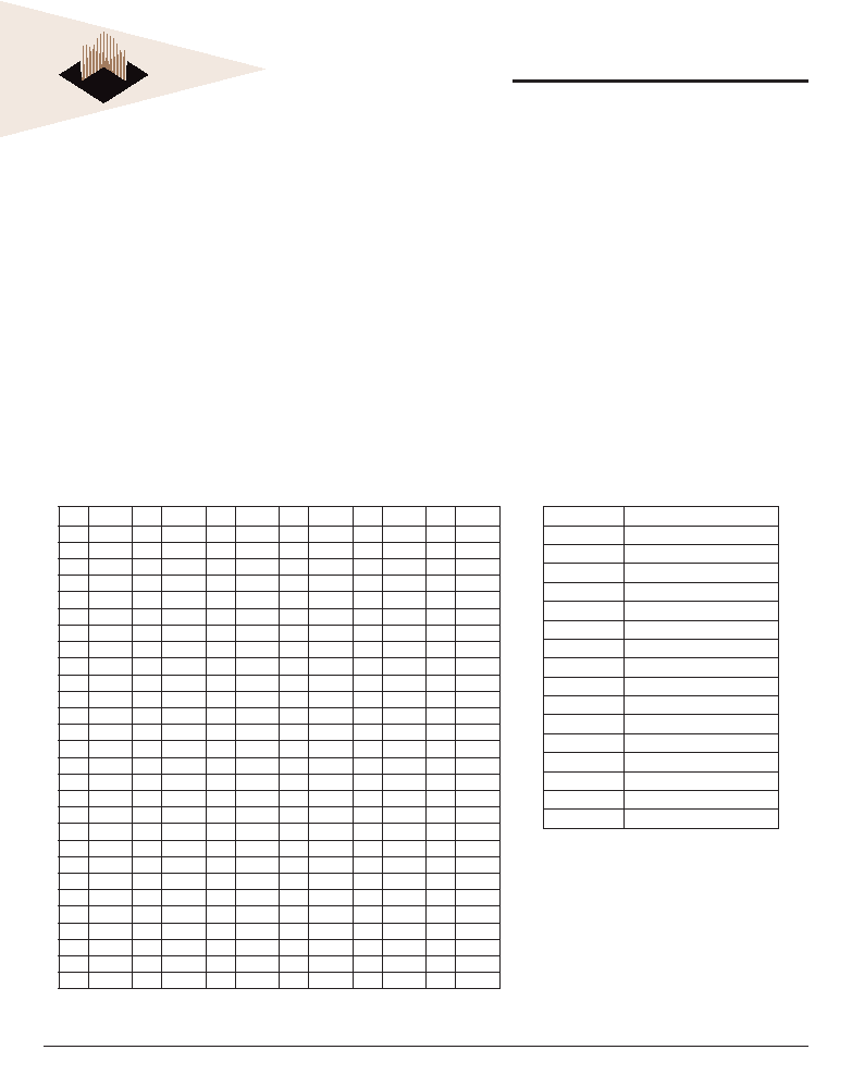
PIN CONFIGURATIONS (FRONT SIDE/BACK SIDE)
Pin
Front
Pin
Front
Pin
Front
Pin
Back
Pin
Back
Pin
Back
1
V
SS
29
DQM1
57
DQ18
85
V
SS
113
DQM5
141
DQ50
2
DQ0
30
CS0#
58
DQ19
86
DQ32
114
NC
142
DQ51
3
DQ1
31
DNU
59
V
CC
87
DQ33
115
RAS#
143
V
CC
4
DQ2
32
V
SS
60
DQ20
88
DQ34
116
V
SS
144
DQ52
5
DQ3
33
A0
61
NC
89
DQ35
117
A1
145
NC
6
V
CC
34
A2
62
NC
90
V
CC
118
A3
146
NC
7
DQ4
35
A4
63
NC
91
DQ36
119
A5
147
NC
8
DQ5
36
A6
64
V
SS
92
DQ37
120
A7
148
V
SS
9
DQ6
37
A8
65
DQ21
93
DQ38
121
A9
149
DQ53
10
DQ7
38
A10/AP
66
DQ22
94
DQ39
122
BA0
150
DQ54
11
DQ8
39
BA1
67
DQ23
95
DQ40
123
A11
151
DQ55
12
V
SS
40
V
CC
68
V
SS
96
V
SS
124
V
CC
152
V
SS
13
DQ9
41
V
CC
69
DQ24
97
DQ41
125
CLK1
153
DQ56
14
DQ10
42
CLK0
70
DQ25
98
DQ42
126
NC
154
DQ57
15
DQ11
43
V
SS
71
DQ26
99
DQ43
127
V
SS
155
DQ58
16
DQ12
44
DNU
72
DQ27
100
DQ44
128
CKE0
156
DQ59
17
DQ13
45
CS2#
73
V
CC
101
DQ45
129
NC
157
V
CC
18
V
CC
46
DQM2
74
DQ28
102
V
CC
130
DQM6
158
DQ60
19
DQ14
47
DQM3
75
DQ29
103
DQ46
131
DQM7
159
DQ61
20
DQ15
48
DNU
76
DQ30
104
DQ47
132
NC
160
DQ62
21
NC
49
V
CC
77
DQ31
105
NC
133
V
CC
161
DQ63
22
NC
50
NC
78
V
SS
106
NC
134
NC
162
V
SS
23
V
SS
51
NC
79
CK2
107
V
SS
135
NC
163
CLK3
24
NC
52
NC
80
NC
108
NC
136
NC
164
NC
25
NC
53
NC
81
NC
109
NC
137
NC
165
SA0
26
V
CC
54
V
SS
82
**SDA
110
V
CC
138
V
SS
166
SA1
27
WE#
55
DQ16
83
**SCL
111
CAS#
139
DQ48
167
SA2
28
DQM0
56
DQ17
84
V
CC
112
DQM4
140
DQ49
168
V
CC
PIN NAMES
A0 ≠ A11
Address input (Multiplexed)
BA0-1
Select Bank
DQ0-63
Data Input/Output
CLK0,CLK3
Clock input
CKE0
Clock Enable input
CS0#-CS2# Chip
select
Input
RAS#
Row Address Strobe
CAS#
Column Address Strobe
WE#
Write Enable
DQM0-7
DQM
V
CC
Power Supply (3.3V)
V
SS
Ground
SDA
Serial data I/O
SCL
Serial clock
DNU
Do not use
NC
No Connect
SA0-SA2
Address in EEPROM
** These pins should be NC in the system which does
not support SPD.

February 2002
Rev. 0
W3DG6430V-D2
2
White Electronic Designs
White Electronic Designs Corporation ∑ (602) 437-1520 ∑ www.wedc.com
PRELIMINARY
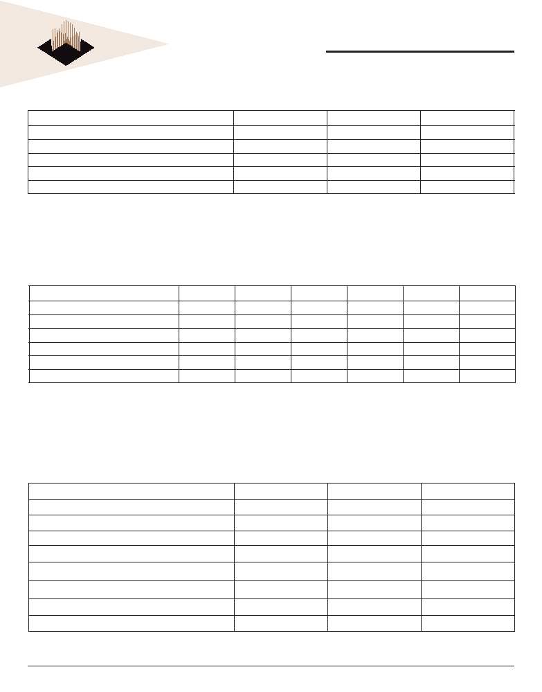
FUNCTIONAL BLOCK DIAGRAM
BA0, BA1, A0 - A11
CS0#
CAS#
RAS#
WE#
CKE0
CS2#
DQ0-3
DQMB0
U1
DQ
DQMB
U3
DQ
DQMB
U2
DQ
DQMB
U4
DQ
DQMB
U7
DQ
DQMB
U5
DQ
DQMB
U6
DQ
DQMB
A
CS#
CAS#
RAS#
W#
CKE
A
CS#
CAS#
RAS#
W#
CKE
A
CS#
CAS#
RAS#
W#
CKE
A
CS#
CAS#
RAS#
W#
CKE
A
CS#
CAS#
RAS#
W#
CKE
A
CS#
CAS#
RAS#
W#
CKE
A
CS#
CAS#
RAS#
W#
CKE
A
CS#
CAS#
RAS#
W#
CKE
A
CS#
CAS#
RAS#
W#
CKE
U8
DQ
DQMB
DQ4-7
DQMB0
DQ8-11
DQMB1
DQ12-15
DQMB1
DQ16-19
DQMB2
DQ20-23
DQMB2
DQ24-27
DQMB3
DQ28-31
DQMB3
U9
DQ
DQMB
U11
DQ
DQMB
U10
DQ
DQMB
U12
DQ
DQMB
U13
DQ
DQMB
U15
DQ
DQMB
U14
DQ
DQMB
U16
DQ
DQMB
DQ60-63
DQMB7
DQ56-59
DQMB7
DQ52-55
DQMB6
DQ48-51
DQMB6
DQ44-47
DQMB5
DQ40-43
DQMB5
DQ36-39
DQMB4
DQ32-35
DQMB4
CLOCK WIRING
INPUT
SDRAMS
CK0
CK1
CK2
CK3
4 SDRAMS
4 SDRAMS
4 SDRAMS
4 SDRAMS
SERIAL PD
SCL
SDA
A0 A1 A2
SA0
SA1
SA2
A
CS#
CAS#
RAS#
W#
CKE
A
CS#
CAS#
RAS#
W#
CKE
A
CS#
CAS#
RAS#
W#
CKE
A
CS#
CAS#
RAS#
W#
CKE
A
CS#
CAS#
RAS#
W#
CKE
A
CS#
CAS#
RAS#
W#
CKE
A
CS#
CAS#
RAS#
W#
CKE
NOTE: A0-A11, BA0-BA1, WE, RAS, CAS, CS0, CS2, CKE0 are buffered,
not registered. 10 ohm registors are in series with all DQ's.
February 2002
Rev. 0
W3DG6430V-D2
3
White Electronic Designs
White Electronic Designs Corporation ∑ (602) 437-1520 ∑ www.wedc.com
PRELIMINARY
ABSOLUTE MAXIMUM RATINGS
Parameter
Symbol
Value
Units
Voltage on any pin relative to V
SS
V
IN
, V
OUT
-1.0 ~ 4.6
V
Voltage on V
CC
supply relative to V
SS
V
CC
, V
CCQ
-1.0 ~ 4.6
V
Storage Temperature
T
STG
-55 ~ +150
∞C
Power Dissipation
P
D
8
W
Short Circuit Current
I
OS
50
mA
Note: Permanent device damage may occur if "ABSOLUTE MAXIMUM RATINGS" are exceeded.
Functional operation should be restricted to recommended operating condition.
Exposure to higher than recommended voltage for extended periods of time could affect device reliability.
RECOMMENDED DC OPERATING CONDITIONS
Voltage Referenced to: V
SS
= 0V, 0∞C T
A
70∞C
Parameter
Symbol
Min
Typ
Max
Unit
Note
Supply Voltage
V
CC
3.0
3.3 3.6
V
Input High Voltage
V
IH
2.0
3.0
V
CC
+0.3
V
Input Low Voltage
V
IL
-0.3
--
0.8
V
Output High Voltage
V
OH
2.4
--
--
V
I
OH
= -2mA
Output Low Voltage
V
OL
--
--
0.4
V
I
OL
= -2mA
Input Leakage Current
I
LI
-20
--
20
A
1
Note: 1. Any input 0V
V
IN
V
CC
Input leakage currents include Hi-Z output leakage for all bi-directional buffers with Tri-State outputs.
CAPACITANCE
T
A
= 23∞C, f = 1MHz, V
CC
= 3.3V, V
REF
=1.4V ± 200mV
Parameter
Symbol
Max
Unit
Input Capacitance (A0-A11)
C
IN1
20
pF
Input Capacitance (RAS#,CAS#,WE#)
C
IN2
20
pF
Input Capacitance (CKE0)
C
IN3
20
pF
Input Capacitance (CLK0,CLK2)
C
IN4
13
pF
Input Capacitance (CS0#,CS2#)
C
IN5
15
pF
Input Capacitance (DQM0-DQM7)
C
IN6
10
pF
Input Capacitance (BA0-BA1)
C
IN7
20
pF
Data input/output capacitance (DQ0-DQ63)
C
OUT
12
pF

February 2002
Rev. 0
W3DG6430V-D2
4
White Electronic Designs
White Electronic Designs Corporation ∑ (602) 437-1520 ∑ www.wedc.com
PRELIMINARY
OPERATING CURRENT CHARACTERISTICS
V
CC
= 3.3V, 0∞C T
A
70∞C
Parameters
Symbol
Conditions
Versions
Units
Note
100
Operating Current
(One bank active)
I
CC1
Burst Length = 1
t
RC
t
RC
(min)
I
OL
= 0mA
1700
mA
1
Precharge Standby Current
in Power Down Mode
I
CC2P
CKE V
IL
(max), t
CC
= 10ns
40
mA
I
CC2PS
CKE & CK V
IL
(max), t
CC
=
40
mA
Precharge Standby Current
in Non-Power Down Mode
I
CC2N
CKE V
IH
(min), CS V
IH
(min), t
CC
=10ns
Input signals are charged one time during 20
350
mA
I
CC2NS
CKE V
IH
(min), CK V
IL
(max), t
CC
=
Input signals are stable
180
mA
Active standby current in power-
down mode
I
CC3P
CKE V
IL
(max), t
CC
= 10ns 90
mA
I
CC3PS
CKE & CK V
IL
(max), t
CC
=
90
Active standby in current non power-
down mode
I
CC3N
CKE V
IH
(min), CS V
IH
(min), t
CC
= 10ns
Input signals are charged one time during 20ns
500
mA
I
CC3NS
CKE V
IH
(min), CK V
IL
(max), t
CC
=
input signals are stable
500
mA
Operating current (Burst mode)
I
CC4
Io = mA
Page burst
4 Banks activated
t
CCD
= 2CK
1700
mA
1
Refresh current
I
CC5
t
RC
t
RC
(min)
3300
mA
2
Self refresh current
I
CC6
CKE 0.2V
40
mA
Notes: 1. Measured with outputs open.
2. Refresh period is 64ms.
3. Unless otherwise noticed, input swing level is CMOS (V
IH
/V
IL
= V
CC
/V
SSQ
)

February 2002
Rev. 0
W3DG6430V-D2
5
White Electronic Designs
White Electronic Designs Corporation ∑ (602) 437-1520 ∑ www.wedc.com
PRELIMINARY
AC CHARACTERISTICS
133MHz component timing
Paramater
Symbol
Min
Max
Units
Notes
Access time from CLK
CL = 2
t
AC
5.4
ns
Address hold time
t
AH
0.8
ns
Address setup time
t
AS
1.5
ns
CLK high level width
t
CH
2.5
ns
CLK low level width
t
CL
2.5
ns
Clock cycle time
CL = 2
t
CK
7.5
ns
1
CKE hold time
t
CKH
0.8
ns
CKE setup time
t
CKS
1.5
ns
CS, RAS, CAS, WE, DQM hold time
t
CMH
0.8
ns
CS, RAS, CAS, WE, DQM setup time
t
CMS
1.5
ns
Data-in hold time
t
DH
0.8
ns
Data-in setup time
t
DS
1.5
ns
Data-out high-impedance time
CL = 2
t
HZ
5.4
ns
2
Data-out low-impedance time
t
LZ
1
ns
Data-out hold time (load)
t
OH
3
ns
Data-out hold time (no load)
t
N
1.8
ns
3
Active to Precharge command
t
RAS
37
120,000
ns
Active to Active command period
t
RC
60
ns
Active to Read or Write delay
t
RCD
15
ns
Refresh period
t
REF
64
ms
Auot refresh period
t
RFC
66
ns
Precharge command period
t
RP
15
ns
Active bank a to Active bank b command
t
RRD
14
ns
Transition time
t
T
0.3
1.2
ns
4
Write recovery time
t
WR
1 CLK + 7ns
ns
5
ns
6
Exit Self Refresh to Active command
t
XSR
67
ns
7
Notes:
1. The clock frequency must remain constant ( stable clock is defi ned as a signal cycling within
timing constraints specifi ed for the clock pin) during access or precharge states (READ,
WRITE, including WR and Precharge commands). CKE may be used to reduce the data rate.
2. t
HZ
defi nes the time at which the output achieves the open circuit condition; it is not a reference
to V
OH
or V
OL
. The last valid data element will meet t
OH
before going High-Z.
3. Paramater guaranteed by design
4. AC characteristics assume t
T
= 1ns
5. Auto precharge mode only) The precharge timing budget ( t
RP
) begins 7ns after the fi rst clock
delay, after the last Write is executed.
6. Precharge mode only.
7. CLK must be toggled a minimum of two times during this period.
MODULE AC CHARACTERISTIC
Symbol
Min
Max
Units
Notes
Address hold time
AH
0
ns
Address setup time
AS
4.5
ns
CS, RAS, CAS, WE, DQM hold time
CMH
0
ns
CS, RAS, CAS, WE, DQM setup time
CMS
4.5
ns
February 2002
Rev. 0
W3DG6430V-D2
6
White Electronic Designs
White Electronic Designs Corporation ∑ (602) 437-1520 ∑ www.wedc.com
PRELIMINARY
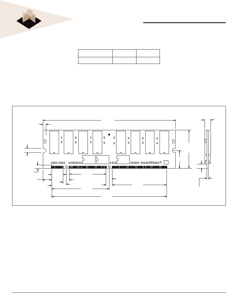
ALL DIMENSIONS ARE IN INCHES
5.250
0.125 (2X)
0.157 (2X)
1.500
MAX.
0.700
0.170 MAX.
0.050 ± 0.004
0.157
MIN.
2.150
0.250
1.450
0.250
2.275
4.550
0.575
0.450
0.000
0.349
0.143
0.000
PACKAGE DIMENSIONS
ORDERING INFORMATION
Part Number
Speed
CAS Latency
W3DG6430V10D2
100MHz
CL=2