
W3DG6433V-JD1
1
White Electronic Designs Corporation ∑ (602) 437-1520 ∑ www.wedc.com
White Electronic Designs
March 2005
Rev. 4
256MB ≠ 32Mx64 SDRAM, UNBUFFERED
FEATURES
Burst Mode Operation
Auto and Self Refresh capability
LVTTL compatible inputs and outputs
Serial Presence Detect with EEPROM
Fully synchronous: All signals are registered on the positive
edge of the system clock
Programmable Burst Lengths: 1, 2, 4, 8 or Full Page
3.3V± 0.3V Power Supply
144
Pin
SO-DIMM
JEDEC
∑ JD1: 31.75 (1.25")
NOTE: Consult factory for availability of:
∑
Lead-Free
Products
∑ Vendor source control options
∑ Industrial temperature option
DESCRIPTION
The W3DG6433V is a 32Mx64 synchronous DRAM module
which consists of four 32Mx16 SDRAM components
in TSOP II package, and one 2Kb EEPROM in an 8
pin TSSOP package for Serial Presence Detect which
are mounted on a 144 pin SO-DIMM multilayer FR4
Substrate.
* This product is subject to change without notice.
PIN NAMES
A0 ≠ A12
Address Input (Multiplexed)
BA0-1
Select Bank
DQ0-63
Data Input/Output
CLK0
Clock Input
CKE0
Clock Enable Input
CS0#
Chip Select Input
RAS#
Row Address Strobe
CAS#
Column Address Strobe
WE#
Write Enable
DQMB0-7
DQM
V
CC
Power Supply (3.3V)
V
SS
Ground
SDA
Serial Data I/O
SCL
Serial Clock
DNU
Do Not Use
NC
No Connect
** These pins should be NC in the system which
does not support SPD.
PIN CONFIGURATIONS (FRONT SIDE/BACK SIDE)
PINOUT
PIN
FRONT
PIN
BACK
PIN
FRONT
PIN
BACK
PIN
BACK
PIN
BACK
1
V
SS
2
V
SS
49
DQ13
50
DQ45
97
DQ22
98
DQ54
3
DQ0
4
DQ32
51
DQ14
52
DQ46
99
DQ23
100
DQ55
5
DQ1
6
DQ33
53
DQ15
54
DQ47
101
V
CC
102
V
CC
7
DQ2
8
DQ34
55
V
SS
56
V
SS
103
A6
104
A7
9
DQ3
10
DQ35
57
NC
58
NC
105
A8
106
BA0
11
V
CC
12
V
CC
59
NC
60
NC
107
V
SS
108
V
SS
13
DQ4
14
DQ36
61
CLK0
62
CKE0
109
A9
110
BA1
15
DQ5
16
DQ37
63
V
CC
64
V
CC
111
A10/AP
112
A11
17
DQ6
18
DQ38
65
RAS#
66
CAS#
113
V
CC
114
V
CC
19
DQ7
20
DQ39
67
WE#
68
NC
115
DQMB2
116
DQMB6
21
V
SS
22
V
SS
69
CS0#
70
A12
117
DQMB3
118
DQMB7
23
DQMB0
24
DQMB4
71
NC
72
NC
119
V
SS
120
V
SS
25
DQMB1
26
DQMB5
73
DNU
74
NC
121
DQ24
122
DQ56
27
V
CC
28
V
CC
75
V
SS
76
V
SS
123
DQ25
124
DQ57
29
A0
30
A3
77
NC
78
NC
125
DQ26
126
DQ58
31
A1
32
A4
79
NC
80
NC
127
DQ27
128
DQ59
33
A2
34
A5
81
V
CC
82
V
CC
129
V
CC
130
V
CC
35
V
SS
36
V
SS
83
DQ16
84
DQ48
131
DQ28
132
DQ60
37
DQ8
38
DQ40
85
DQ17
86
DQ49
133
DQ29
134
DQ61
39
DQ9
40
DQ41
87
DQ18
88
DQ50
135
DQ30
136
DQ62
41
DQ10
42
DQ42
89
DQ19
90
DQ51
137
DQ31
138
DQ63
43
DQ11
44
DQ43
91
V
SS
92
V
SS
139
V
SS
140
V
SS
45
V
CC
46
V
CC
93
DQ20
94
DQ52
141
SDA**
142
SCL**
47
DQ12
48
DQ44
95
DQ21
96
DQ53
143
V
CC
144
V
CC

W3DG6433V-JD1
2
White Electronic Designs Corporation ∑ (602) 437-1520 ∑ www.wedc.com
White Electronic Designs
March 2005
Rev. 4
FUNCTIONAL BLOCK DIAGRAM
V
CC
Vss
To all SDRAMs
A0 ~ A12
CKE0
RAS#
CAS#
WE#
SDRAM
SDRAM
SDRAM
SDRAM
SDRAM
SDRAM
SDRAM
CLK0
SDRAM
SDRAM
Serial PD
SDA
SCL
SA1 SA2
SA0
WP
47K
10
10
CS0#
DQMB0
DQMB1
DQ0
DQ1
DQ2
DQ3
DQ4
DQ5
DQ6
DQ7
DQ0
DQ1
DQ2
DQ3
DQ4
DQ5
DQ6
DQ7
DQ8
DQ9
DQ10
DQ11
DQ12
DQ13
DQ14
DQ15
DQ8
DQ9
DQ10
DQ11
DQ12
DQ13
DQ14
DQ15
LDQM CS#
UDQM
DQ0
DQ1
DQ2
DQ3
DQ4
DQ5
DQ6
DQ7
U2
DQ32
DQ33
DQ34
DQ35
DQ36
DQ37
DQ38
DQ39
DQ8
DQ9
DQ10
DQ11
DQ12
DQ13
DQ14
DQ15
DQ40
DQ41
DQ42
DQ43
DQ44
DQ45
DQ46
DQ47
LDQM CS#
UDQM
DQMB2
DQMB3
DQ0
DQ1
DQ2
DQ3
DQ4
DQ5
DQ6
DQ7
DQ16
DQ17
DQ18
DQ19
DQ20
DQ21
DQ22
DQ23
DQ8
DQ9
DQ10
DQ11
DQ12
DQ13
DQ14
DQ15
DQ24
DQ25
DQ26
DQ27
DQ28
DQ29
DQ30
DQ31
LDQM CS#
UDQM
DQMB7
DQ0
DQ1
DQ2
DQ3
DQ4
DQ5
DQ6
DQ7
DQ48
DQ49
DQ50
DQ51
DQ52
DQ53
DQ54
DQ55
DQ8
DQ9
DQ10
DQ11
DQ12
DQ13
DQ14
DQ15
DQ56
DQ57
DQ58
DQ59
DQ60
DQ61
DQ62
DQ63
LDQM CS#
UDQM
DQMB4
DQMB5
DQMB6
BA0 & 1
SDRAM
Note: All resistor values are 10 ohms unless otherwise specifi ed.

W3DG6433V-JD1
3
White Electronic Designs Corporation ∑ (602) 437-1520 ∑ www.wedc.com
White Electronic Designs
March 2005
Rev. 4
ABSOLUTE MAXIMUM RATINGS
Parameter
Symbol
Value
Units
Voltage on any pin relative to V
SS
V
IN
, V
OUT
-1.0 ~ 4.6
V
Voltage on V
CC
supply relative to V
SS
V
CC
, V
CCQ
-1.0 ~ 4.6
V
Storage Temperature
T
STG
-55 ~ +150
∞C
Power Dissipation
P
D
4 W
Short Circuit Current
I
OS
50
mA
Note:
Permanent device damage may occur if "ABSOLUTE MAXIMUM RATINGS" are exceeded.
Functional operation should be restricted to recommended operating condition.
Exposure to higher than recommended voltage for extended periods of time could affect device reliability.
RECOMMENDED DC OPERATING CONDITIONS
Voltage Referenced to: V
SS
= 0V, T
A
= 0∞C to +70∞C
Parameter
Symbol
Min
Typ
Max
Unit
Note
Supply Voltage
V
CC
3.0
3.3 3.6
V
Input High Voltage
V
IH
2.0
3.0
V
CCQ+0.3
V
1
Input Low Voltage
V
IL
-0.3
--
0.8
V
2
Output High Voltage
V
OH
2.4
--
--
V
I
OH
= -2mA
Output Low Voltage
V
OL
--
--
0.4
V
I
OL
= -2mA
Input Leakage Current
I
LI
-10
--
10
µA
3
Note:
1. V
IH
(max) = 5.6V AC. The overshoot voltage duration is 3ns.
2. V
IL
(min) = -2.0V AC. The undershoot voltage duration is 3ns.
3.
Any input 0V V
IN
V
CCQ
Input leakage currents include Hi-Z output leakage for all bi-directional buffers with Tri-State outputs.
CAPACITANCE
T
A
= 25∞C, f = 1MHz, V
CC
= 3.3V, V
REF
= 1.4V ± 200mV
Parameter
Symbol
Max
Unit
Input Capacitance (A0-A12)
C
IN1
21
pF
Input Capacitance (RAS#,CAS#,WE#)
C
IN2
21
pF
Input Capacitance (CKE0)
C
IN3
21
pF
Input Capacitance (CLK0)
C
IN4
16
pF
Input Capacitance (CS0#)
C
IN5
21
pF
Input Capacitance (DQM0-DQM7)
C
IN6
11
pF
Input Capacitance (BA0-BA1)
C
IN7
21
pF
Data Input/Output Capacitance (DQ0-DQ63)
C
OUT
9
pF

W3DG6433V-JD1
4
White Electronic Designs Corporation ∑ (602) 437-1520 ∑ www.wedc.com
White Electronic Designs
March 2005
Rev. 4
OPERATING CURRENT CHARACTERISTICS
V
CC
= 3.3V, 0∞C
T
A
+70∞C
Version
Parameter
Symbol
Conditions
133
100
Units
Note
Operating Current
(One bank active)
I
CC1
Burst Length = 1
t
RC
t
RC
(min)
I
OL
= 0mA
440
440
mA
1
Precharge Standby Current
in Power Down Mode
I
CC2P
CKE
V
IL
(max), t
CC
= 10ns
14
mA
Active Standby Current in
Non-Power Down Mode
I
CC3N
CKE
V
IH
(min), CS
V
IH
(min), tcc = 10ns Input
signals are changed one time during 20ns
180
mA
Operating Current (Burst mode)
I
CC4
Io = mA
Page burst
4 Banks activated
t
CCD
= 2CK
520
520
mA
1
Refresh Current
I
CC5
t
RC
t
RC
(min)
980
980
mA
2
Self Refresh Current
I
CC6
CKE
0.2V
24
mA
Notes:
1.
Measured with outputs open.
2.
Refresh period is 64ms.

W3DG6433V-JD1
5
White Electronic Designs Corporation ∑ (602) 437-1520 ∑ www.wedc.com
White Electronic Designs
March 2005
Rev. 4
AC OPERATING TEST CONDITIONS
V
CC
= 3.3V ± 0.3V, 0 T
A
70∞C
Parameter
Value
Unit
AC input levels (V
IH
/V
IL
)
2.4/0.4
V
Input timing measurement reference level
1.4
V
Input rise and fall time
t
R
/t
F
= 1/1
ns
Output timing measurement reference level
1.4
V
OPERATING AC PARAMETER
(AC operating conditions unless otherwise noted)
Parameter
Symbol
Version
Unit
Note
7.5, 10
Row active to row active delay
t
RRD
(min)
15
ns
1
RAS# to CAS# delay
t
RCD
(min)
20
ns
1
Row precharge time
t
RP
(min)
20
ns
1
Row active time
t
RAS
(min)
45
ns
1
t
RAS
(max)
100
us
Row cycle time
t
RC
(min)
65
ns
1
Last data in to row precharge
t
RDL
(min)
2
CLK
2
Last data in to Active delay
t
DAL
(min)
2 CLK + t
RP
--
Last data in to new col. address delay
t
CDL
(min)
1
CLK
2
Last data in to burst stop
t
BDL
(min)
1
CLK
2
Col. address to col. address delay
t
CCD
(min)
1
CLK
3
Number of valid output data
CAS latency=3
2
ea
4
CAS latency=2
1
Notes :
1.
The minimum number of clock cycles is determined by dividing the minimum time required with clock cycle time and then rounding off to the next higher integer.
2.
Minimum delay is required to complete write.
3.
All parts allow every cycle column address change.
4.
In case of row precharge interrupt, auto precharge and read burst stop.

W3DG6433V-JD1
6
White Electronic Designs Corporation ∑ (602) 437-1520 ∑ www.wedc.com
White Electronic Designs
March 2005
Rev. 4
PART NUMBERING GUIDE
W 3 D G 64 33 V xxx JD1 x F/G
WEDC
SDRAM MEMORY
SINGLE DATA RATE
GOLD
DEPTH x64
DENSITY
3.3 Volts
SPEED (MHz)
PACKAGE
COMPONENT VENDOR
NAME
(M = Micron)
(S = Samsung)
F = LEAD-FREE,
G = RoHS COMPLIANT
W3DG6433V-JD1
7
White Electronic Designs Corporation ∑ (602) 437-1520 ∑ www.wedc.com
White Electronic Designs
March 2005
Rev. 4
NOTES:
∑ Consult Factory for availability of Lead-Free products. (F = Lead-Free, G = RoHS Compliant)
∑ Product specifi c part numbers are available for source control if needed, please consult factory for the correct part
number if a specifi c component vendor is preferred. Please add "-M" for Micron or "-S" for Samsung to the back of the
part number for the specifi c component vendor preferred.
∑ Consult factory for availability of industrial temperature (-40∞C to 85∞C) option
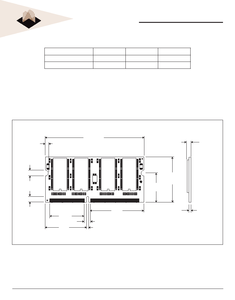
Ordering Information
Speed
CAS Latency
Height*
W3DG6433V10JD1
100MHz
CL=2
31.75 (1.25")
W3DG6433V75JD1
133MHz
CL=3
31.75 (1.25")
PACKAGE DIMENSIONS FOR JD1
31.75
(1.25)
Max
3.99
(0.157)
4.00
(0.157)
2.01 (0.079 Min)
67.59
(2.661 Max)
32.79
(1.291)
4.60 (0.181)
1.50 (0.059)
28.2
(1.112)
23.14
(0.913)
20.00
(0.787)
2.54
(0.10)
MAX.
9.91
(0.039)
(± 0.004)
PACKAGE DIMENSIONS FOR JD1
* ALL DIMENSIONS ARE IN MILLIMETERS AND (INCHES).

W3DG6433V-JD1
8
White Electronic Designs Corporation ∑ (602) 437-1520 ∑ www.wedc.com
White Electronic Designs
March 2005
Rev. 4
Document Title
256MB ≠ 32Mx64 SDRAM UNBUFFERED
Revision History
Rev #
History
Release Date
Status
Rev 0
Created
11-01
Advanced
Rev 1
1.1 Removed "ED" from part number
1.2 Updated CAP and I
DD
specs
6-04
Preliminary
Rev 2
2.1 Updated block diagram
2.2 Updated package dimensions
2.3 Added lead-free and RoHS notes
2.4 Added source control options
2.5 Added industrial temperature option
2.6 Added AC Specs
1-05
Preliminary
Rev 3
3.1 Updated ICC Specs
3.2 Move from Preliminary to Final
1-05
Final
Rev 4
4.1 Redesigned PCB to handle series resistors and to meet
JEDEC
4.2
Package height changed from 1.10" to 1.25"
4.3 Added solder mask for short protection
4.4
Changed package designation from D1 to JD1
4.5 Added part number matrix
4-05
Final