W3DG7266V-D2
1
White Electronic Designs Corporation ∑ (602) 437-1520 ∑ www.wedc.com
White Electronic Designs
May 2005
Rev. 3
White Electronic Designs Corp. reserves the right to change products or specifi cations without notice.
PRELIMINARY*
512MB ≠ 64Mx72 SDRAM, REGISTER and SPD, w/PLL
DESCRIPTION
The W3DG7266V is a 64Mx72 synchronous DRAM
module which consists of nine 64Mx8 SDRAM components
in TSOP II package, two 18 bit Drive ICs for input control
signal and one 2Kb EEPROM in an 8 pin TSSOP package
for Serial Presence Detect which are mounted on a 168
pin DIMM mul ti lay er FR4 Substrate.
* This product is under development, is not qualifi ed or characterized and is subject to
change without notice.
NOTE: Consult factory for availability of:
∑
Lead-Free
Products
∑ Vendor source control options
∑ Industrial temperature option
FEATURES
Burst
Mode
Operation
Auto and Self Refresh capability
LVTTL compatible inputs and outputs
Serial Presence Detect with EEPROM
Fully synchronous: All signals are registered on the positive
edge of the system clock
Programmable Burst Lengths: 1, 2, 4, 8 or Full Page
3.3V
± 0.3V Power Supply
168 Pin DIMM JEDEC
∑ PCB: 30.49mm (1.20") MAX
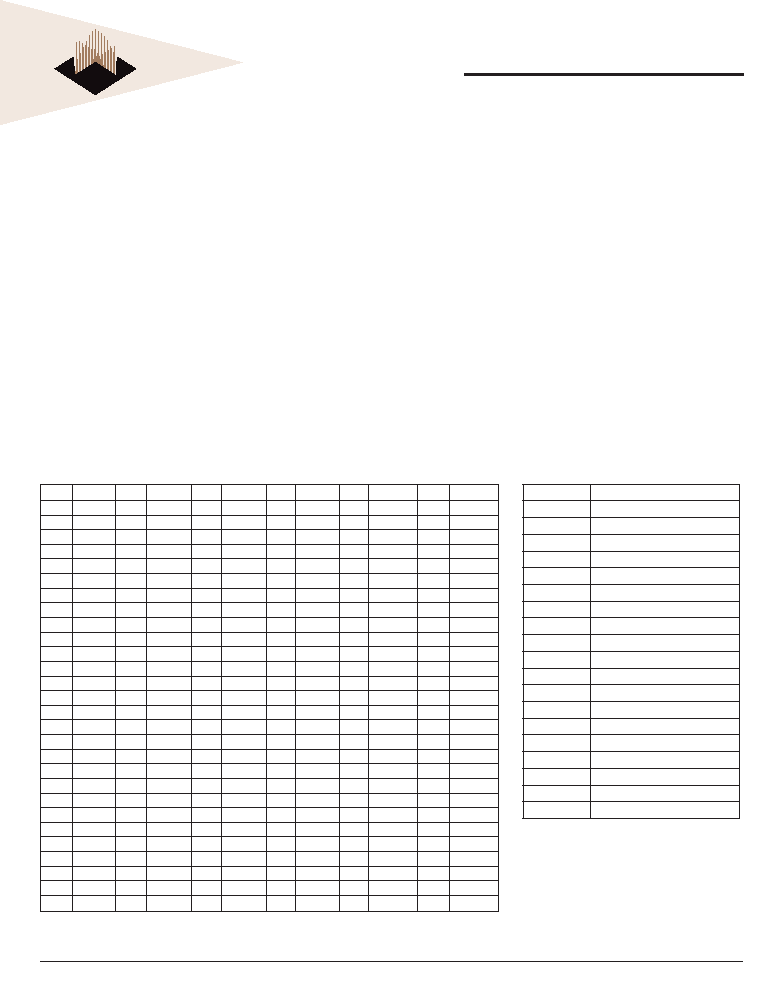
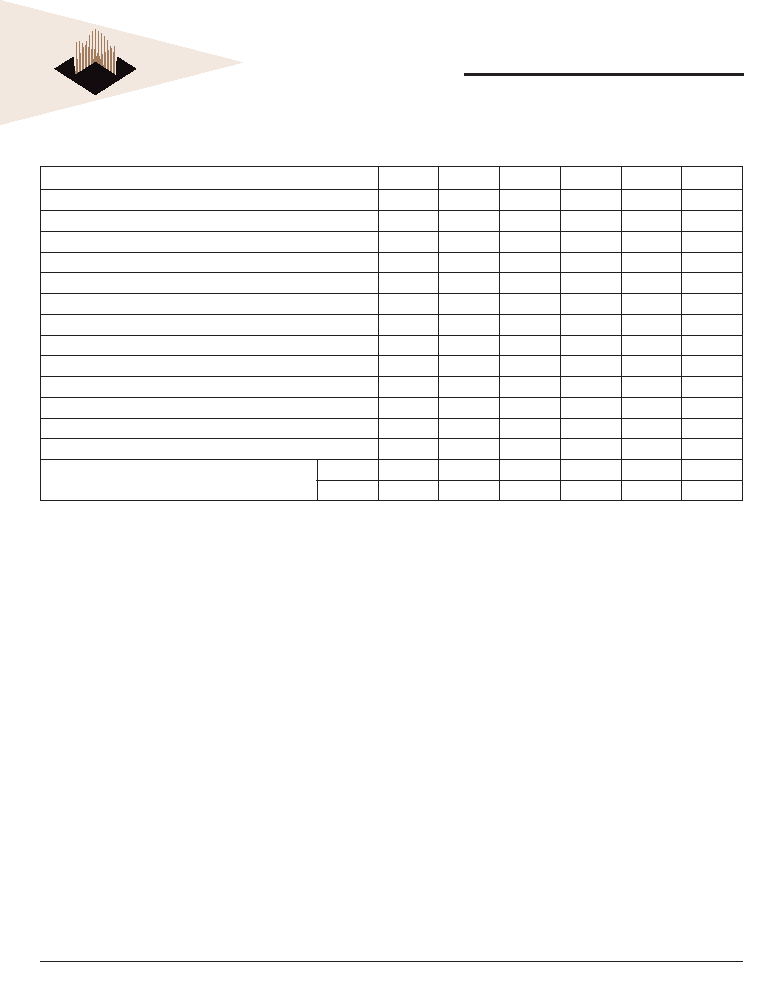
PIN NAMES
A0 ≠ A12
Address Input (Multiplexed)
BA0-1
Select Bank
DQ0-63
Data Input/Output
CB0-7
Check Bit (Data-In/Data-Out)
CK0
Clock Input
CKE0
Clock Enable Input
CS0#, CS2#
Chip Select Input
RAS#
Row Address Strobe
CAS#
Column Address Strobe
WE#
Write Enable
DQM0-7
DQM
V
CC
Power Supply (3.3V)
V
SS
Ground
*V
REF
Power Supply for Reference
REGE
Register Enable
SDA
Serial Data I/O
SCL
Serial Clock
SA0-2
Address in EEPROM
DNU
Do Not Use
NC
No Connect
* These pins are not used in this module.
** These pins should be NC in the system which does
not support SPD.
PIN CONFIGURATIONS (FRONT SIDE/BACK SIDE)
PIN
FRONT
PIN
BACK
PIN
FRONT
PIN
BACK
PIN
BACK
PIN
BACK
1
V
SS
29
DQM1
57
DQ18
85
V
SS
113
DQM5
141
DQ50
2
DQ0
30
CS0#
58
DQ19
86
DQ32
114
*CS1#
142
DQ51
3
DQ1
31
DNU
59
V
CC
87
DQ33
115
RAS#
143
V
CC
4
DQ2
32
V
SS
60
DQ20
88
DQ34
116
V
SS
144
DQ52
5
DQ3
33
A0
61
NC
89
DQ35
117
A1
145
NC
6
V
CC
34
A2
62
*V
REF
90
V
CC
118
A3
146
*V
REF
7
DQ4
35
A4
63
*CKE1
91
DQ36
119
A5
147
REGE
8
DQ5
36
A6
64
V
SS
92
DQ37
120
A7
148
V
SS
9
DQ6
37
A8
65
DQ21
93
DQ38
121
A9
149
DQ53
10
DQ7
38
A10/AP
66
DQ22
94
DQ39
122
BA0
150
DQ54
11
DQ8
39
BA1
67
DQ23
95
DQ40
123
A11
151
DQ55
12
V
SS
40
V
CC
68
V
SS
96
V
SS
124
V
CC
152
V
SS
13
DQ9
41
V
CC
69
DQ24
97
DQ41
125
*CK1
153
DQ56
14
DQ10
42
CK0
70
DQ25
98
DQ42
126
A12
154
DQ57
15
DQ11
43
V
SS
71
DQ26
99
DQ43
127
V
SS
155
DQ58
16
DQ12
44
DNU
72
DQ27
100
DQ44
128
CKE0
156
DQ59
17
DQ13
45
CS2#
73
V
CC
101
DQ45
129
*CS3#
157
V
CC
18
V
CC
46
DQM2
74
DQ28
102
V
CC
130
DQM6
158
DQ60
19
DQ14
47
DQM3
75
DQ29
103
DQ46
131
DQM7
159
DQ61
20
DQ15
48
DNU
76
DQ30
104
DQ47
132
*A13
160
DQ62
21
CB0
49
V
CC
77
DQ31
105
CB4
133
V
CC
161
DQ63
22
CB1
50
NC
78
V
SS
106
CB5
134
NC
162
V
SS
23
V
SS
51
NC
79
*CK2
107
V
SS
135
NC
163
*CK3
24
NC
52
CB2
80
NC
108
NC
136
CB6
164
NC
25
NC
53
CB3
81
NC
109
NC
137
CB7
165
**SA0
26
V
CC
54
V
SS
82
**SDA
110
V
CC
138
V
SS
166
**SA1
27
WE#
55
DQ16
83
**SCL
111
CAS#
139
DQ48
167
*SA2
28
DQM0
56
DQ17
84
V
CC
112
DQM4
140
DQ49
168
V
CC
W3DG7266V-D2
2
White Electronic Designs Corporation ∑ (602) 437-1520 ∑ www.wedc.com
White Electronic Designs
May 2005
Rev. 3
White Electronic Designs Corp. reserves the right to change products or specifi cations without notice.
PRELIMINARY
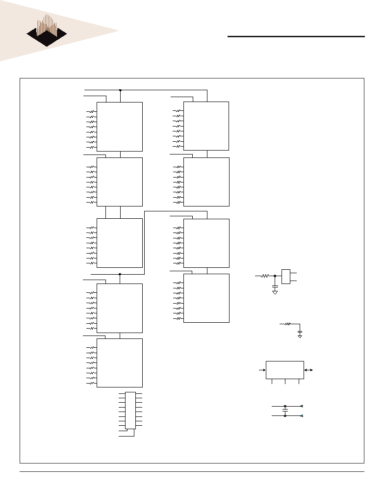
FUNCTIONAL BLOCK DIAGRAM
REGE
PCK
DQMB3
DQMB2
DQ0
DQ1
DQ2
DQ3
DQM
I/O 0
I/O 1
I/O 2
I/O 3
DQMB0
DQ4
DQ5
DQ6
DQ7
I/O 4
I/O 5
I/O 6
I/O 7
DQ8
DQ9
DQ10
DQ11
DQM
I/O 0
I/O 1
I/O 2
I/O 3
DQ12
DQ13
DQ14
DQ15
I/O 4
I/O 5
I/O 6
I/O 7
DQ16
DQ17
DQ18
DQ19
DQM
I/O 0
I/O 1
I/O 2
I/O 3
DQ20
DQ21
DQ22
DQ23
I/O 4
I/O 5
I/O 6
I/O 7
DQ24
DQ25
DQ26
DQ27
DQM
I/O 0
I/O 1
I/O 2
I/O 3
DQ28
DQ29
DQ30
DQ31
I/O 4
I/O 5
I/O 6
I/O 7
DQ40
DQ41
DQ42
DQ43
DQM
I/O 0
I/O 1
I/O 2
I/O 3
DQMB4
DQ44
DQ45
DQ46
DQ47
I/O 4
I/O 5
I/O 6
I/O 7
DQ48
DQ49
DQ50
DQ51
DQM
I/O 0
I/O 1
I/O 2
I/O 3
DQ52
DQ53
DQ54
DQ55
I/O 4
I/O 5
I/O 6
I/O 7
DQ56
DQ57
DQ58
DQ59
DQM
I/O 0
I/O 1
I/O 2
I/O 3
DQ60
DQ61
DQ62
DQ63
I/O 4
I/O 5
I/O 6
I/O 7
CB0
CB1
CB2
CB3
DQM
I/O 0
I/O 1
I/O 2
I/O 3
CB4
CB5
CB6
CB7
I/O 4
I/O 5
I/O 6
I/O 7
DQMB1
DQ32
DQ33
DQ34
DQ35
DQM
I/O 0
I/O 1
I/O 2
I/O 3
DQ36
DQ37
DQ38
DQ39
I/O 4
I/O 5
I/O 6
I/O 7
DQMB5
DQMB6
DQMB7
#
CS0#
CS
CS
CS
CS
CS
CS
CS
CS
CS
CS2#
V
CC
V
SS
SDRAM
SDRAM
* Wire per Clock Loading Table/Wiring Diagrams
NOTE: DQ wiring may differ than described in
this drawing, however DQ/DQMB/CKE/S
relationships must be maintained as shown.
CS0# - CS2#
DQMB0 - DQMB7
BA0 - BA1
A0 - A12
RAS#
CAS#
CKE0
WE#
RCS0# - RCS2#
RDQMB0 - RDQMB7
RRAS#: SDRAMS
RCAS#: SDRAMS
RCKE0: SDRAMS
RWE#: SDRAMS
R
E
G
I
S
T
E
R
RBA0 - RBA1: SDRAMS
RA0 - RA12: SDRAMS
A0
SERIAL PD
A1
A2
SA0
SA1
SA2
SCL
CK1-CK3
SDA
12pF
12pF
10ohm
10ohm
PLL
PLL
CK0
SDRAM
10 ohm
REGISTER
12pF
12pF
NOTE: All resistor values are 10 ohms.
W3DG7266V-D2
3
White Electronic Designs Corporation ∑ (602) 437-1520 ∑ www.wedc.com
White Electronic Designs
May 2005
Rev. 3
White Electronic Designs Corp. reserves the right to change products or specifi cations without notice.
PRELIMINARY
ABSOLUTE MAXIMUM RATINGS
Parameter
Symbol
Value
Units
Voltage on any pin relative to V
SS
V
IN
, V
OUT
-1.0 ~ 4.6
V
Voltage on V
CC
supply relative to V
SS
V
CC
, V
CCQ
-1.0 ~ 4.6
V
Storage Temperature
T
STG
-55 ~ +150
∞C
Power Dissipation
P
D
18
W
Short Circuit Current
I
OS
50
mA
Note: Permanent device damage may occur if "ABSOLUTE MAXIMUM RATINGS" are exceeded.
Functional operation should be restricted to recommended operating condition.
Exposure to higher than recommended voltage for extended periods of time could affect device reliability.
RECOMMENDED DC OPERATING CONDITIONS
Voltage Referenced to: V
SS
= 0V, 0∞C T
A
70∞C
Parameter
Symbol
Min
Typ
Max
Unit
Note
Supply Voltage
V
CC
3.0
3.3 3.6
V
Input High Voltage
V
IH
2.0
3.0
V
CCQ
+0.3
V
1
Input Low Voltage
V
IL
-0.3
--
0.8
V
2
Output High Voltage
V
OH
2.4
--
--
V
I
OH
= -2mA
Output Low Voltage
V
OL
--
--
0.4
V
I
OL
= -2mA
Input Leakage Current
I
LI
-10
--
10
A
3
Note: 1. V
IH
(max)= 5.6V AC. The overshoot voltage duration is
3ns.
2. V
IL
(min)= -2.0V AC. The undershoot voltage duration is
3ns.
3. Any input 0V V
IN
V
CCQ
Input leakage currents include Hi-Z output leakage for all bi-directional buffers with Tri-State outputs.
CAPACITANCE
T
A
= 25 ∞C, f = 1MHz, V
CC
= 3.3V, V
REF
= 1.4V ± 200mV
Parameter
Symbol
Max
Unit
Input Capacitance (A0-A11)
C
IN1
9
pF
Input Capacitance (RAS#,CAS#,WE#)
C
IN2
9
pF
Input Capacitance (CKE0)
C
IN3
9
pF
Input Capacitance (CLK0)
C
IN4
6
pF
Input Capacitance (CS0#,CS2#)
C
IN5
9
pF
Input Capacitance (DQM0-DQM7)
C
IN6
7
pF
Input Capacitance (BA0-BA1)
C
IN7
9
pF
Data input/output capacitance (DQ0-DQ63)
C
OUT
9
pF
Data input/output capacitance (CB0-CB7)
C
OUT1
9
pF
W3DG7266V-D2
4
White Electronic Designs Corporation ∑ (602) 437-1520 ∑ www.wedc.com
White Electronic Designs
May 2005
Rev. 3
White Electronic Designs Corp. reserves the right to change products or specifi cations without notice.
PRELIMINARY
OPERATING CURRENT CHARACTERISTICS
V
CC
= 3.3V, 0∞C
T
A
70∞C
Parameters
Symbol
Conditions
Versions
Units
Note
133/100
Operating Current
(One bank active)
I
CC1
Burst Length = 1
t
RC
t
RC
(min)
I
OL
= 0mA
1080
mA
1
Standby Current
in Power Down Mode
I
CC2
C
KE
V
IL
(max), t
CC
= 10ns
32
mA
Active standby in current non power-down
mode
I
CC3
C
KE
V
IH
(min), CS V
IH
(min), t
CC
= 10ns
Input signals are charged one time during 20ns
405
mA
Operating current (Burst mode)
I
CC4
Io = mA
Page burst
4 Banks activated
t
CCD
= 2CLK
1125
mA
1
Refresh current
I
CC5
t
RC
t
RC
(min)
2295
mA
2
Self refresh current
I
CC6
C
KE
0.2V
54
mA
Notes: 1. Measured with outputs open.
2. Refresh period is 64ms.

W3DG7266V-D2
5
White Electronic Designs Corporation ∑ (602) 437-1520 ∑ www.wedc.com
White Electronic Designs
May 2005
Rev. 3
White Electronic Designs Corp. reserves the right to change products or specifi cations without notice.
PRELIMINARY
ELECTRICAL CHARACTERISTICS AND RECOMMENDED AC OPERATING CONDITIONS
V
CC
, V
CCQ
= +3.3V ±0.3V
AC CHARACTERISTICS
SYMBOL
7
7.5
10
UNITS
NOTE
PARAMETER
MIN
MAX
MIN
MAX
MIN
MAX
Access timefrom CLK (pos.edge)
CL = 3
t
AC(3)
5.4
5.4
6
ns
27
CL = 2
t
AC(2)
5.4
6
6
ns
Address hold time
t
AH
0.8
0.8
1
ns
Address setup time
t
AS
1.5
1.5
2
ns
CLK high-level width
t
CH
2.5
2.5
3
ns
CLK low-level width
t
CL
2.5
2.5
3
ns
Clock cycle time
CL = 3
t
CK(3)
7
7.5
8
ns
23
CL = 2
t
CK(2)
7.5
10
10
ns
23
CKE hold time
t
CKH
0.8
0.8
1
ns
CKE setup time
t
CKS
1.5
1.5
2
ns
CS#, RAS#, CAS#, WE#, DQM hold time
t
CMH
0.8
0.8
1
ns
CS#, RAS#, CAS#, WE#, DQM setup time
t
CMS
1.5
1.5
2
ns
Data-in hold time
t
DH
0.8
0.8
1
ns
Data-in setup time
t
DS
1.5
1.5
2
ns
Data-out high-impedance time
CL = 3
t
HZ(3)
5.4
5.4
6
ns
10
CL = 2
t
HZ(2)
5.4
6
6
ns
10
Data-out low-impedance time
t
LZ
1
1
1
ns
Data-out hold time (load)
t
OH
2.7
2.7
2.7
ns
Data-out hold time (no load)
t
OHN
1.8
1.8
1.8
ns
28
ACTIVE to PRECHARGE command
t
RAS
37
120,000
44
120,000
50
120,000
ns
ACTIVE to ACTIVE command period
t
RC
60
66
66
ns
ACTIVE to READ or WRITE delay
t
RCD
15
20
20
ns
Refresh period
t
REF
64
64
64
ms
AUTOREFRESH period
t
RFC
66
66
66
ns
PRECHARGE command period
t
RP
15
20
20
ns
ACTIVE bank a to ACTIVE bank b command
t
RRD
14
15
15
ns
Transition time
t
T
0.3
1.2
0.3
1.2
0.3
1.2
ns
7
WRITE recovery time
t
WR
1 CLK
+
7ns
1 CLK
+
7.5ns
1 CLK
+
7.5ns
24
14
15
15
ns
25
Exit SELF REFRESH to ACTIVE command
t
XSR
67
75
80
ns
20
W3DG7266V-D2
6
White Electronic Designs Corporation ∑ (602) 437-1520 ∑ www.wedc.com
White Electronic Designs
May 2005
Rev. 3
White Electronic Designs Corp. reserves the right to change products or specifi cations without notice.
PRELIMINARY
AC FUNCTIONAL CHARACTERISTICS
V
CC
, V
CCQ
= +3.3V ±0.3V
PARAMETER
SYMBOL
7
7.5
10
UNITS
NOTES
READ/WRITE command to READ/WRITE command
t
CCD
1
1
1
t
CK
17
CKE to clock disable or power-down entry mode
t
CKED
1
1
1
t
CK
14
CKE to clock enable or power-down exit setup mode
t
PED
1
1
1
t
CK
14
DQM to input data delay
t
DQD
0
0
0
t
CK
17
DQM to data mask during WRITEs
t
DQM
0
0
0
t
CK
17
DQMto data high-impedance during READs
t
DQZ
2
2
2
t
CK
17
WRITE command to input data delay
t
DWD
0
0
0
t
CK
17
Data-into ACTIVE command
t
DAL
4
5
5
t
CK
15, 21
Data-into PRECHARGE command
t
DPL
2
2
2
t
CK
16, 21
Last data-in to burst STOP command
t
BDL
1
1
1
t
CK
17
Last data-in to new READ/WRITE command
t
CDL
1
1
1
t
CK
17
Lastdata-into PRECHARGE command
t
RDL
2
2
2
t
CK
16, 21
LOADMODEREGISTER command to ACTIVE or REFRESH command
t
MRD
2
2
2
t
CK
26
Data-out to high-impedance from PRECHARGE command
CL = 3
t
ROH(3)
3
3
3
t
CK
17
CL = 2
t
ROH(2)
2
2
2
t
CK
17

W3DG7266V-D2
7
White Electronic Designs Corporation ∑ (602) 437-1520 ∑ www.wedc.com
White Electronic Designs
May 2005
Rev. 3
White Electronic Designs Corp. reserves the right to change products or specifi cations without notice.
PRELIMINARY
Notes
1.
All voltages referenced to V
SS
.
2.
This parameter is sampled. V
CC
, V
CCQ
= +3.3V; T
A
= 25∞C; pin under test biased
at 1.4V; f = 1 MHz.
3. I
DD
is dependent on output loading and cycle rates. Specifi ed values are obtained
with mini-mum cycle time and the outputs open.
4.
Enables on-chip refresh and address counters.
5.
The minimum specifi cations are used only to indicate cycle time at which proper
operation over the full temperature range is ensured.
6.
An initial pause of 100µs is required after power-up, followed by two AUTO
REFRESH commands, before proper device operation is ensured. (V
CC
and V
CCQ
must be powered up simultaneously. V
SS
and V
SSQ
must be at same potential.)
The two AUTO REFRESH command wake-ups should be repeated any time the
tREF refresh requirement is exceeded.
7.
AC characteristics assume t
T
= 1ns.
8.
In addition to meeting the transition rate specifi cation, the clock and CKE must
transit between V
IH
and V
IL
(or between V
IL
and V
IH
) in a mono-tonic manner.
9.
Outputs measured at 1.5V with equivalent load:
Q
50pF
10. t
HZ
defi nes the time at which the output achieves the open circuit condition; it is
not a reference to V
OH
or V
OL
. The last valid data element will meet t
OH
before
going High-Z.
11.
AC timing and I
DD
tests have V
IL
= 0V and V
IH
= 3V with timing referenced to 1.5V
crossover point. If the input transition time is longer than 1ns, then the timing is
referenced at V
IL
(MAX) and V
IH
(MIN) and no longer at the 1.5V crossover point.
12.
Other input signals are allowed to transition no more than once every two clocks
and are other-wise at valid V
IH
or V
IL
levels.
13. I
DD
specifi cations are tested after the device is properly initialized.
14.
Timing actually specifi ed by t
CKS
; clock(s) specifi ed as a reference only at
minimum cycle rate.
15.
Timing actually specifi ed by t
WR
plus t
RP
; clock(s) specifi ed as a reference only at
minimum cycle rate.
16.
Timing actually specifi ed by t
WR
.
17.
Required clocks are specifi ed by JEDEC functionality and are not dependent on
any timing parameter.
18. The
I
DD
current will increase or decrease proportionally according to the amount
of frequency alteration for the test condition.
19.
Address transitions average one transition every two clocks.
20.
CLK must be toggled a minimum of two times during this period.
21.
Based on t
CK
= 10ns for 10, and t
CK
= 7.5ns for 7 and 7.5.
22. V
IH
overshoot: V
IH
(MAX) = V
CCQ
+ 2V for a pulse width 3ns, and the pulse
width cannot be greater than one third of the cycle rate. V
IL
under-shoot: V
IL
(MIN) = -2V for a pulse width 3ns.
23.
The clock frequency must remain constant (stable clock is defi ned as a signal
cycling within timing constraints specifi ed for the clock pin) during access or
precharge states (READ, WRITE, including t
WR
, and PRECHARGE commands).
CKE may be used to reduce the data rate.
24.
Auto precharge mode only. The precharge timing budget (t
RP
) begins 7ns for 7;
7.5ns for 7.5 and 7.5ns for 10 after the fi rst clock delay, after the last WRITE is
executed. May not exceed limit set for precharge mode.
25. Precharge
mode
only.
26.
JEDEC and PC133, PC100 specify three clocks.
27. t
AC
for 7/7.5 at CL = 3 with no load is 4.6ns and is guaranteed by design.
28.
Parameter guaranteed by design.
W3DG7266V-D2
8
White Electronic Designs Corporation ∑ (602) 437-1520 ∑ www.wedc.com
White Electronic Designs
May 2005
Rev. 3
White Electronic Designs Corp. reserves the right to change products or specifi cations without notice.
PRELIMINARY
17.78
(0.700)
30.48
(1.20)
MAX.
3.99
(0.157)
MIN.
1.27 ± 0.10
(0.050 ± 0.004)
MEASURED AFTER
PLATING
OVER FINGERS.
4.32
(0.170)
MAX.
133.48 (5.255)
MAX.
SEE NOTE 1
54.61
(2.150)
6.35
(0.250)
115.57
(4.550)
42.19
(1.661)
36.83
(1.450)
6.35
(0.250)
3.18
(0.125)
(2X)
15.60
(0.614)
11.43
(0.450)
3.99
(0.157)
(2X)
ALL DIMENSIONS ARE IN MILLIMETERS AND (INCHES)
PACKAGE DIMENSIONS
ORDERING INFORMATION FOR D2
Part Number
Speed
CAS Latency
Height*
W3DG7266V10D2
100MHz
CL=2
30.48 (1.20")
W3DG7266V7D2
133MHz
CL=2
30.48 (1.20")
W3DG7266V75D2
133MHz
CL=3
30.48 (1.20")
NOTES:
∑ Consult Factory for availability of Lead-Free products. (F = Lead-Free, G = RoHS Compliant)
∑ Vendor specifi c part numbers are used to provide memory components source control. The place holder for this is
shown as lower case "x" in the part numbers above and is to be replaced with the respective vendors code. Consult
factory for qualifi ed sourcing options. (M = Micron, S = Samsung & consult factory for others)
∑ Consult factory for availability of industrial temperature (-40∞C to 85∞C) option

W3DG7266V-D2
9
White Electronic Designs Corporation ∑ (602) 437-1520 ∑ www.wedc.com
White Electronic Designs
May 2005
Rev. 3
White Electronic Designs Corp. reserves the right to change products or specifi cations without notice.
PRELIMINARY
Document Title
512MB ≠ 64Mx72 SDRAM, REGISTER and SPD, w/PLL
Revision History
Rev #
History
Release Date
Status
Rev A
Create
2-21-02
Advanced
Rev 1
1.1 Updated CAP and I
DD
Specs
1.2 Removed "ED" from part number
1.3 Added new title page
1.4 Moved from Advanced to Preliminary
8-2004
Preliminary
Rev 2
2.1 Added AC specs
3.2 Provided lead-free and RoHS notes
2.3 Added source control notes
2.4 Added industiral temperature note
2-05
Preliminary
Rev 3
3.1 Updated CAP specs
3.2 Updated I
DD
specs
5-05
Preliminary