1
White Electronic Designs Corporation ∑ (602) 437-1520 ∑ www.wedc.com
White Electronic Designs
W3EG72128S-AD4
-BD4
August 2005
Rev. 3
PRELIMINARY*
OPERATING FREQUENCIES
DDR333 @CL=2.5
DDR266 @CL=2
DDR266 @CL=2.5
DDR200 @CL=2
Clock Speed
166MHz
133MHz
133MHz
100MHz
CL-t
RCD
-t
RP
2.5-3-3
2-2-2
2.5-3-3
2-2-2
1GB ≠ 2x64Mx72 DDR SDRAM UNBUFFERED ECC w/PLL
FEATURES
Double-data-rate
architecture
DDR200, DDR266 and DDR333
Bi-directional data strobes (DQS)
Differential clock inputs (CK & CK#)
Programmable Read Latency 2,2.5 (clock)
Programmable Burst Length (2,4,8)
Programmable Burst type (sequential & interleave)
Edge aligned data output, center aligned data input
Auto and self refresh
Serial presence detect
Dual
Rank
Power supply: 2.5V ± 0.20V
JEDEC standard 200 pin SO-DIMM package
∑ Package height options:
AD4: 35.5 mm (1.38") and
BD4: 31.75 mm (1.25")
NOTE: Consult factory for availability of:
∑ RoHS compliant products
∑ Vendor source control options
∑ Industrial temperature option
DESCRIPTION
The W3EG72128S is a 2x64Mx72 Double Data Rate
SDRAM memory module based on 512Mb DDR SDRAM
components. This module consists of eighteen 64Mx8 bit
DDR SDRAMs in 66 pin TSOP packages mounted on a
200 pin FR4 substrate.
Synchronous design allows precise cycle control with the
use of system clock. Data I/O transactions are possible on
both edges and Burst Lengths allow the same device to be
useful for a variety of high bandwidth, high performance
memory system ap pli ca tions.
* This product is under development, is not qualifi ed or characterized and is subject to
change without notice.
2
White Electronic Designs Corporation ∑ (602) 437-1520 ∑ www.wedc.com
White Electronic Designs
W3EG72128S-AD4
-BD4
August 2005
Rev. 3
PRELIMINARY
PIN#
SYMBOL
PIN#
SYMBOL
PIN#
SYMBOL
PIN#
SYMBOL
1
V
REF
51
V
SS
101
A9
151
DQ42
2
V
REF
52
V
SS
102
A8
152
DQ46
3
V
SS
53
DQ19
103
V
SS
153
DQ43
4
V
SS
54
DQ23
104
V
SS
154
DQ47
5
DQ0
55
DQ24
105
A7
155
V
CC
6
DQ4
56
DQ28
106
A6
156
V
CC
7
DQ1
57
V
CC
107
A5
157
V
CC
8
DQ5
58
V
CC
108
A4
158
NC
9
V
CC
59
DQ25
109
A3
159
V
SS
10
V
CC
60
DQ29
110
A2
160
NC
11
DQS0
61
DQS3
111
A1
161
V
SS
12
DQM0
62
DQM3
112
A0
162
V
SS
13
DQ2
63
V
SS
113
V
CC
163
DQ48
14
DQ6
64
V
SS
114
V
CC
164
DQ52
15
V
SS
65
DQ26
115
A10/AP
165
DQ49
16
V
SS
66
DQ30
116
BA1
166
DQ53
17
DQ3
67
DQ27
117
BA0
167
V
CC
18
DQ7
68
DQ31
118
RAS#
168
V
CC
19
DQ8
69
V
CC
119
WE#
169
DQS6
20
DQ12
70
V
CC
120
CAS#
170
DQM6
21
V
CC
71
CB0
121
CS0#
171
DQ50
22
V
CC
72
CB4
122
CS1#
172
DQ54
23
DQ9
73
CB1
123
NC
173
V
SS
24
DQ13
74
CB5
124
NC
174
V
SS
25
DQS1
75
V
SS
125
V
SS
175
DQ51
26
DQM1
76
V
SS
126
V
SS
176
DQ55
27
V
SS
77
DQS8
127
DQ32
177
DQ56
28
V
SS
78
DQM8
128
DQ36
178
DQ60
29
DQ10
79
NC
129
DQ33
179
V
CC
30
DQ14
80
CB6
130
DQ37
180
V
CC
31
DQ11
81
V
CC
131
V
CC
181
DQ57
32
DQ15
82
V
CC
132
V
CC
182
DQ61
33
V
CC
83
CB3
133
DQS4
183
DQS7
34
V
CC
84
CB7
134
DQM4
184
DQM7
35
CK0
85
NC
135
DQ34
185
V
SS
36
V
CC
86
NC
136
DQ38
186
V
SS
37
CK0#
87
V
SS
137
V
SS
187
DQ58
38
V
SS
88
V
SS
138
V
SS
188
DQ62
39
V
SS
89
NC
139
DQ35
189
DQ59
40
V
SS
90
V
SS
140
DQ39
190
DQ63
41
DQ16
91
NC
141
DQ40
191
V
CC
42
DQ20
92
V
CC
142
DQ44
192
V
CC
43
DQ17
93
V
CC
143
V
CC
193
SDA
44
DQ21
94
V
CC
144
V
CC
194
SA0
45
V
CC
95
CKE1
145
DQ41
195
SCL
46
V
CC
96
CKE0
146
DQ45
196
SA1
47
DQS2
97
NC
147
DQS5
197
V
CCSPD
48
DQM2
98
NC
148
DQM5
198
SA2
49
DQ18
99
A12
149
V
SS
199
V
CCID
50
DQ22
100
A11
150
V
SS
200
NC
PIN CONFIGURATION
A0-A12
Address input (Multiplexed)
BA0-BA1
Bank Select Address
DQ0-DQ63
Data Input/Output
DQS0-DQS8
Data Strobe Input/Output
CK0
Clock Input
CK0#
Clock Input
CKE0, CKE1
Clock Enable input
CS0#, CS1#
Chip Select Input
RAS#
Row Address Strobe
CAS#
Column Address Strobe
WE#
Write Enable
DQM0-DQM8
Data-In Mask
V
CC
Power Supply (2.5V)
V
SS
Ground
V
REF
Power Supply for Reference
V
CCSPD
Serial EEPROM Power Supply
(2.3V to 3.6V)
SDA
Serial data I/O
SCL
Serial clock
SA0-SA2
Address in EEPROM
V
CCID
V
CC
Indentifi cation Flag
NC
No Connect
PIN NAMES
3
White Electronic Designs Corporation ∑ (602) 437-1520 ∑ www.wedc.com
White Electronic Designs
W3EG72128S-AD4
-BD4
August 2005
Rev. 3
PRELIMINARY
FUNCTIONAL BLOCK DIAGRAM
DQS2
DQM2
DQ8
DQ9
DQ10
DQ11
DQ12
DQ13
DQ14
DQ15
DQ0
DQ1
DQ2
DQ3
DQ4
DQ5
DQ6
DQ7
DM
CS#
DQS
CS#
DQS3
DQM3
DQ16
DQ17
DQ18
DQ19
DQ20
DQ21
DQ22
DQ23
DQ0
DQ1
DQ2
DQ3
DQ4
DQ5
DQ6
DQ7
DM
CS#
DQS
CS#
DQS8
DQM8
DQ24
DQ25
DQ26
DQ27
DQ28
DQ29
DQ30
DQ31
DQ0
DQ1
DQ2
DQ3
DQ4
DQ5
DQ6
DQ7
DM
CS#
DQS
CS#
CB0
CB1
CB2
CB3
CB4
CB5
CB6
CB7
DQ0
DQ1
DQ2
DQ3
DQ4
DQ5
DQ6
DQ7
DM
CS#
DQS
CS#
DQS1
DQM1
DQ0
DQ1
DQ2
DQ3
DQ4
DQ5
DQ6
DQ7
DQ0
DQ1
DQ2
DQ3
DQ4
DQ5
DQ6
DQ7
DM
CS#
DQS
CS#
DQS5
DQM5
DQ32
DQ33
DQ34
DQ35
DQ36
DQ37
DQ38
DQ39
DQ0
DQ1
DQ2
DQ3
DQ4
DQ5
DQ6
DQ7
DM
CS#
DQS
CS#
DQS6
DQM6
DQ40
DQ41
DQ42
DQ43
DQ44
DQ45
DQ46
DQ47
DQ0
DQ1
DQ2
DQ3
DQ4
DQ5
DQ6
DQ7
DM
CS#
DQS
CS#
DQS7
DQM7
DQ48
DQ49
DQ50
DQ51
DQ52
DQ53
DQ54
DQ55
DQ0
DQ1
DQ2
DQ3
DQ4
DQ5
DQ6
DQ7
DM
CS#
DQS
CS#
DQ56
DQ57
DQ58
DQ59
DQ60
DQ61
DQ62
DQ63
DQ0
DQ1
DQ2
DQ3
DQ4
DQ5
DQ6
DQ7
DM
CS#
DQS
CS#
CS1#
CS0#
DQS0
DQM0
DQS4
DQM4
RAS#
RAS#
CAS#
CAS#
BA0-BA1
BA0-BA1
WE#
WE#
A0-A12
A0-A12
CKE0
CKE0
CKE1
CKE1
RAS: DDR SDRAMs
RAS: DDR SDRAMs
CAS: DDR SDRAMs
CAS: DDR SDRAMs
BA0-BA1: DDR SDRAMs
BA0-BA1: DDR SDRAMs
WE: DDR SDRAMs
WE: DDR SDRAMs
A0-A12: DDR SDRAMs
A0-A12: DDR SDRAMs
CKE0: DDR SDRAMs
CKE0: DDR SDRAMs
CKE1: DDR SDRAMs
CKE1: DDR SDRAMs
SERIAL PD
SCL
SDA
A0
A1
A2
SA0
SA1
SA2
DDR SDRAM
DDR SDRAM
DDR SDRAM
DDR SDRAM
V
CC
CC
GND
GND
120
PLL
PLL
V
CC
CK0
CLK0/CLK0#
CLK1/CLK1#
CLK2/CLK2#
CLK3/CLK3#
CK0#
CK0A
CK0A#
FEEDBACK
Note: All datalines are terminated through a 22 ohms series resistor.
4
White Electronic Designs Corporation ∑ (602) 437-1520 ∑ www.wedc.com
White Electronic Designs
W3EG72128S-AD4
-BD4
August 2005
Rev. 3
PRELIMINARY
ABSOLUTE MAXIMUM RATINGS
Parameter
Symbol
Value
Units
Voltage on any pin relative to V
SS
V
IN
, V
OUT
-0.5 to 3.6
V
Voltage on V
CC
supply relative to V
SS
V
CC
, V
CCQ
-1.0 to 3.6
V
Storage Temperature
T
STG
-55 to +150
∞C
Power Dissipation
P
D
9
W
Short Circuit Current
I
OS
50
mA
Note:
Permanent device damage may occur if "ABSOLUTE MAXIMUM RATINGS" are exceeded.
Functional operation should be restricted to recommended operating condition.
Exposure to higher than recommended voltage for extended periods of time could affect device reliability.
DC CHARACTERISTICS
0∞C
T
A
70∞C, V
CC
= 2.5V ± 0.2V
CAPACITANCE
T
A
= 25∞C, f = 1MHz, V
CC
= 3.3V, V
REF
=1.4V ± 200mV
Parameter
Symbol
Min
Max
Unit
Supply Voltage
V
CC
2.3
2.7
V
Supply Voltage
V
CCQ
2.3
2.7
V
Reference Voltage
V
REF
V
CCQ/2
- 50mV
V
CCQ/2
+ 50mV
V
Termination Voltage
V
TT
V
REF
- 0.04
V
REF
+ 0.04
V
Input High Voltage
V
IH
V
REF
+ 0.15
V
CCQ
+ 0.3
V
Input Low Voltage
V
IL
-0.3
V
REF
- 0.15
V
Output High Voltage
V
OH
V
TT
+ 0.76
--
V
Output Low Voltage
V
OL
--
V
TT
- 0.76
V
Parameter
Symbol
Max
Unit
Input Capacitance (A0-A12)
C
IN1
56
pF
Input Capacitance (RAS#, CAS#, WE#)
C
IN2
56
pF
Input Capacitance (CKE0)
C
IN3
29
pF
Input Capacitance (CK0,CK0#)
C
IN4
5.5
pF
Input Capacitance (CS0#)
C
IN5
29
pF
Input Capacitance (DQM0-DQM8)
C
IN6
13
pF
Input Capacitance (BA0-BA1)
C
IN7
56
pF
Data input/output capacitance (DQ0-DQ63)(DQS)
C
OUT
13
pF

5
White Electronic Designs Corporation ∑ (602) 437-1520 ∑ www.wedc.com
White Electronic Designs
W3EG72128S-AD4
-BD4
August 2005
Rev. 3
PRELIMINARY
IDD SPECIFICATIONS AND TEST CONDITIONS
Recommended operating conditions, 0∞C
T
A
70∞C, V
CCQ
= 2.5V ± 0.2V, V
CC
= 2.5V ± 0.2V
Parameter
Symbol Conditions
DDR333@CL=2.5
Max
DDR266@CL=2
Max
DDR266@CL=2.5
Max
DDR200@CL=2
Max
Units
Operating Current
I
DD0
One device bank; Active - Precharge;
t
RC
=t
RC
(MIN); t
CK
=t
CK
(MIN); DQ,DM
and DQS inputs changing once per
clock cycle; Address and control
inputs changing once every two
cycles.
2620
2620
2620
2620
mA
Operating Current
I
DD1
One device bank; Active-Read-
Precharge; Burst = 2; t
RC
=t
RC
(MIN)
;t
CK
=t
CK
(MIN); Iout = 0mA; Address
and control inputs changing once per
clock cycle.
2890
2890
2890
2890
mA
Precharge Power-
Down Standby Current
I
DD2P
All device banks idle; Power- down
mode; t
CK
=t
CK
(MIN); CKE=(low)
90
90
90
90
mA
Idle Standby Current
I
DD2F
CS# = High; All device banks idle;
t
CK
=t
CK
(MIN); CKE = high; Address
and other control inputs changing
once per clock cycle. Vin = Vref for
DQ, DQS and DM.
1085
1085
1085
1085
mA
Active Power-Down
Standby Current
I
DD3P
One device bank active; Power-down
mode; t
CK
(MIN); CKE=(low)
630
630
630
630
mA
Active Standby Current
I
DD3N
CS# = High; CKE = High; One
device bank; Active-Precharge;
t
RC
=t
RAS
(MAX); t
CK
=t
CK
(MIN); DQ,
DM and DQS inputs changing twice
per clock cycle; Address and other
control inputs changing once per
clock cycle.
1175
1175
1175
1175
mA
Operating Current
I
DD4R
Burst = 2; Reads; Continous burst;
One device bank active;Address
and control inputs changing once
per clock cycle; t
CK
=t
CK
(MIN); Iout
= 0mA.
2935
2935
2935
2935
mA
Operating Current
I
DD4W
Burst = 2; Writes; Continous burst;
One device bank active; Address
and control inputs changing once per
clock cycle; t
CK
=t
CK
(MIN); DQ,DM
and DQS inputs changing twice per
clock cycle.
3025
2845
2845
2845
mA
Auto Refresh Current
I
DD5
t
RC
=t
RC
(MIN)
4060
4060
4060
4060
mA
Self Refresh Current
I
DD6
CKE
0.2V
360
365
365
365
mA
Operating Current
I
DD7A
Four bank interleaving Reads (BL=4)
with auto precharge with t
RC
=t
RC
(MIN); t
CK
=t
CK
(MIN); Address and
control inputs change only during
Active Read or Write commands.
5095
5050
5050
5050
mA

6
White Electronic Designs Corporation ∑ (602) 437-1520 ∑ www.wedc.com
White Electronic Designs
W3EG72128S-AD4
-BD4
August 2005
Rev. 3
PRELIMINARY
I
DD1
: OPERATING CURRENT : ONE BANK
1. Typical
Case
:
V
CC
=2.5V, T=25∞C
2. Worst
Case
:
V
CC
=2.7V, T=10∞C
3. Only one bank is accessed with t
RC
(min), Burst
Mode, Address and Control inputs on NOP edge
are changing once per clock cycle. I
OUT
= 0mA
4. Timing
Patterns
:
∑
DDR200 (100 MHz, CL=2) : t
CK=
10ns, CL2,
BL=4, t
RCD=
2*t
CK
, t
RAS=
5*t
CK
Read : A0 N R0 N N P0 N A0 N - repeat the
same timing with random address changing;
50% of data changing at every burst
∑
DDR266 (133MHz, CL=2.5) : t
CK=
7.5ns,
CL=2.5, BL=4, t
RCD=
3*t
CK
, t
RC=
9*t
CK
, t
RAS=
5*t
CK
Read : A0 N N R0 N P0 N N N A0 N - repeat
the same timing with random address
changing; 50% of data changing at every burst
∑
DDR266 (133MHz, CL=2) : t
CK
=7.5ns, CL=2,
BL=4, t
RCD
=3*t
CK
, t
RC
=9*t
CK
, t
RAS
=5*t
CK
Read : A0 N N R0 N P0 N N N A0 N - repeat
the same timing with random address
changing; 50% of data changing at every burst
∑
DDR333 (166MHz, CL=2.5) : t
CK
=6ns, BL=4,
t
RCD
=10*t
CK
, t
RAS
=7*t
CK
Read : A0 N N R0 N P0 N N N A0 N - repeat
the same timing with random address
changing; 50% of data changing at every burst
I
DD7A
: OPERATING CURRENT : FOUR BANKS
1. Typical
Case
:
V
CC
=2.5V, T=25∞C
2. Worst
Case
:
V
CC
=2.7V, T=10∞C
3. Four banks are being interleaved with t
RC
(min),
Burst Mode, Address and Control inputs on NOP
edge are not changing. Iout=0mA
4. Timing
Patterns
:
∑
DDR200 (100 MHz, CL=2) : t
CK
=10ns, CL2,
BL=4, t
RRD
=2*t
CK
, t
RCD
=3*t
CK
, Read with
Autoprecharge
Read : A0 N A1 R0 A2 R1 A3 R2 A0 R3 A1 R0
- repeat the same timing with random address
changing; 100% of data changing at every
burst
∑
DDR266 (133MHz, CL=2.5) : t
CK
=7.5ns,
CL=2.5, BL=4, t
RRD
=3*t
CK
, t
RCD
=3*t
CK
Read with Autoprecharge
Read : A0 N A1 R0 A2 R1 A3 R2 N R3 A0 N
A1 R0 - repeat the same timing with random
address changing; 100% of data changing at
every burst
∑
DDR266 (133MHz, CL=2) : t
CK
=7.5ns, CL2=2,
BL=4, t
RRD
=2*t
CK
, t
RCD
=2*t
CK
Read : A0 N A1 R0 A2 R1 A3 R2 N R3 A0 N
A1 R0 - repeat the same timing with random
address changing; 100% of data changing at
every burst
∑
DDR333 (166MHz, CL=2.5) : t
CK
=6ns,
BL=4, t
RRD
=3*t
CK
, t
RCD
=3*t
CK
, Read with
Autoprecharge
Read : A0 N A1 R0 A2 R1 A3 R2 N R3 A0 N
A1 R0 - repeat the same timing with random
address changing; 100% of data changing at
every burst
DETAILED TEST CONDITIONS FOR DDR SDRAM I
DD1
& I
DD7A
Legend : A = Activate, R = Read, W = Write, P = Precharge, N = NOP
A (0-3) = Activate Bank 0-3
R (0-3) = Read Bank 0-3

7
White Electronic Designs Corporation ∑ (602) 437-1520 ∑ www.wedc.com
White Electronic Designs
W3EG72128S-AD4
-BD4
August 2005
Rev. 3
PRELIMINARY
DDR SDRAM COMPONENT ELECTRICAL CHARACTERISTICS AND RECOMMENDED
AC OPERATING CONDITIONS
AC CHARACTERISTICS
335
262
265/202
PARAMETER
SYMBOL
MIN
MAX
MIN
MAX
MIN
MAX
UNITS
NOTES
Access window of DQs from CK/CK#
t
AC
-0.70
+0.70
-0.75
+0.75
-0.75
0.75
ns
CK high-level width
t
CH
0.45
0.55
0.45
0.55
0.45
0.55
t
CK
26
CK low-level width
t
CL
0.45
0.55
0.45
0.55
0.45
0.55
t
CK
26
Clock cycle time
CL = 2.5
t
CK (2.5)
6
13
7.5
13
7.5
13
ns
39, 44
CL = 2
t
CK (2)
7.5
13
7.5
13
7.5/10
13
ns
39, 44
DQ and DM input hold time relative to DQS
t
DH
0.45
0.5
0.5
ns
23, 27
DQ and DM input setup time relative to DQS
t
DS
0.45
0.5
0.5
ns
23, 27
DQ and DM input pulse width (for each input)
t
DIPW
1.75
1.75
1.75
ns
27
Access window of DQS from CK/CK#
t
DQSCK
-0.60
+0.60
-0.75
+0.75
-0.75
+0.75
ns
DQS input high pulse width
t
DQSH
0.35
0.35
0.35
t
CK
DQS input low pulse width
t
DQSL
0.35
0.35
0.35
t
CK
DQS-DQ skew, DQS to last DQ valid, per group, per
access
t
DQSQ
0.4
0.5
0.5
ns
22, 23
Write command to fi rst DQS latching transition
t
DQSS
0.75
1.25
0.75
1.25
0.75
1.25
t
CK
DQS falling edge to CK rising - setup time
t
DSS
0.20
0.20
0.2
t
CK
DQS falling edge from CK rising - hold time
t
DSH
0.20
0.20
0.2
t
CK
Half clock period
t
HP
t
CH,
t
CL
t
CH,
t
CL
t
CH,
t
CL
ns
30
Data-out high-impedance window from CK/CK#
t
HZ
+0.70
+0.75
+0.75
ns
16, 36
Data-out low-impedance window from CK/CK#
t
LZ
-0.70
-0.75
-0.75
ns
16, 36
Address and control input hold time (fast slew rate)
t
IHF
0.75
0.90
0.90
ns
12
Address and control input setup time (fast slew rate)
t
ISF
0.75
0.90
0.90
ns
12
Address and control input hold time (slow slew rate)
t
IHS
0.8
1
1
ns
12

8
White Electronic Designs Corporation ∑ (602) 437-1520 ∑ www.wedc.com
White Electronic Designs
W3EG72128S-AD4
-BD4
August 2005
Rev. 3
PRELIMINARY
DDR SDRAM COMPONENT ELECTRICAL CHARACTERISTICS AND RECOMMENDED
AC OPERATING CONDITIONS (Continued)
AC CHARACTERISTICS
335
262
265/202
PARAMETER
SYMBOL
MIN
MAX
MIN
MAX
MIN
MAX
UNITS
NOTES
Address and control input setup time (slow slew rate)
t
ISS
0.8
1
1
ns
12
Address and Control input pulse width (for each input)
t
IPW
2.2
2.2
2.2
ns
LOAD MODE REGISTER command cycle time
t
MRD
12
15
15
ns
DQ-DQS hold, DQS to fi rst DQ to go non-valid, per access
t
QH
t
HP -
t
QHS
t
HP -
t
QHS
t
HP -
t
QHS
ns
22, 23
Data hold skew factor
t
QHS
0.50
0.75
0.75
ns
ACTIVE to PRECHARGE command
t
RAS
42
70,000
40
120,000
40
120,000
ns
30, 47
ACTIVE to READ with Auto precharge command
t
RAP
15
15
20
ns
ACTIVE to ACTIVE/AUTO REFRESH command period
t
RC
60
60
65
ns
AUTO REFRESH command period
t
RFC
72
75
78
ns
42
ACTIVE to READ or WRITE delay
t
RCD
15
15
20
ns
PRECHARGE command period
t
RP
15
15
20
ns
DQS read preamble
t
RPRE
0.9
1.1
0.9
1.1
0.9
1.1
t
CK
37
DQS read postamble
t
RPST
0.4
0.6
0.4
0.6
0.4
0.6
t
CK
37
ACTIVE bank a to ACTIVE bank b command
t
RRD
12
15
15
ns
DQS write preamble
t
WPRE
0.25
0.25
0.25
t
CK
DQS write preamble setup time
t
WPRES
0
0
0
ns
18, 19
DQS write postamble
t
WPST
0.4
0.6
0.4
0.6
0.4
0.6
t
CK
17
Write recovery time
t
WR
15
15
15
ns
Internal WRITE to READ command delay
t
WTR
1
1
1
t
CK
Data valid output window
NA
t
QH -
t
DQSQ
t
QH -
t
DQSQ
t
QH -
t
DQSQ
ns
22
REFRESH to REFRESH command interval
t
REFC
70.3
70.3
70.3
µs
21
Average periodic refresh interval
t
REFI
7.8
7.8
7.8
µs
21
Terminating voltage delay to V
CC
t
VTD
0
0
0
ns
Exit SELF REFRESH to non-READ command
t
XSNR
75
75
75
ns
Exit SELF REFRESH to READ command
t
XSRD
200
200
200
t
CK
9
White Electronic Designs Corporation ∑ (602) 437-1520 ∑ www.wedc.com
White Electronic Designs
W3EG72128S-AD4
-BD4
August 2005
Rev. 3
PRELIMINARY
Notes
1.
All voltages referenced to V
SS
.
2.
Tests for AC timing, I
DD
, and electrical AC and DC characteristics may be
conducted at nominal reference/supply voltage levels, but the related specifi cations
and device operation are guaranteed for the full voltage range specifi ed.
3.
Outputs measured with equivalent load:
Output
Output
(V
(V
OUT
OUT
)
Reference
Reference
Point
Point
50
50
V
TT
TT
30pF
30pF
4.
AC timing and I
DD
tests may use a V
IL
-to-V
IH
swing of up to 1.5V in the test
environment, but input timing is still referenced to V
REF
(or to the crossing point for
CK/CK#), and parameter specifi cations are guaranteed for the specifi ed AC input
levels under normal use conditions. The mini-mum slew rate for the input signals
used to test the device is 1V/ns in the range between V
IL
(AC) and V
IH
(AC).
5.
The AC and DC input level specifi cations are as defi ned in the SSTL_2 Standard
(i.e., the receiver will effectively switch as a result of the signal crossing the AC
input level, and will remain in that state as long as the signal does not ring back
above [below] the DC input LOW [HIGH] level).
6. V
REF
is expected to equal V
CCQ/2
of the transmitting device and to track variations
in the DC level of the same. Peak-to-peak noise (non-common mode) on V
REF
may
not exceed ±2 percent of the DC value. Thus, from V
CCQ/2
, V
REF
is allowed ±25mV
for DC error and an additional ±25mV for AC noise. This measurement is to be
taken at the nearest V
REF
bypass capacitor.
7. V
TT
is not applied directly to the device. V
TT
is a system supply for signal
termination resistors, is expected to be set equal to V
REF
and must track variations
in the DC level of V
REF
.
8. I
DD
is dependent on output loading and cycle rates. Specifi ed values are obtained
with mini-mum cycle time at CL = 2 for 262, and 263, CL = 2.5 for 335 and 265 with
the outputs open.
9.
Enables on-chip refresh and address counters.
10. I
DD
specifi cations are tested after the device is properly initialized, and is averaged
at the defi ned cycle rate.
11. This parameter is sampled. V
CC
= +2.5V ±0.2V, V
CC
Q = +2.5V ±0.2V, V
REF
= VSS,
f = 100 MHz, T
A
= 25∞C, V
OUT
(DC) = V
CCQ/2
, V
OUT
(peak to peak) = 0.2V. DM input
is grouped with I/O pins, refl ecting the fact that they are matched in loading.
12. For slew rates < 1 V/ns and to 0.5 Vns. If the slew rate is < 0.5V/ns, timing
must be derated: t
IS
has an additional 50ps per each 100 mV/ns reduction in slew
rate from 500mV/ns, while t
IH
is unaffected. If the slew rate exceeds 4.5 V/ns,
functionality is uncertain. For 335, slew rates must be 0.5 V/ns.
13. The CK/CK# input reference level (for timing referenced to CK/CK#) is the point at
which CK and CK# cross; the input reference level for signals other than CK/CK# is
V
REF
.
14. Inputs are not recognized as valid until V
REF
stabilizes. Exception: during the period
before V
REF
stabilizes, CKE < 0.3 x V
CCQ
is recognized as LOW.
15. The output timing reference level, as measured at the timing reference point
indicated in Note 3, is V
TT
.
16. t
HZ
and t
LZ
transitions occur in the same access time windows as valid data
transitions. These parameters are not referenced to a specifi c voltage level, but
specify when the device output is no longer driving (HZ) or begins driving (LZ).
17. The intent of the Don't Care state after completion of the postamble is the DQS-
driven signal should either be high, low, or high-Z and that any signal transition
within the input switching region must follow valid input requirements. That is, if
DQS transitions high (above V
IH
DC (MIN) then it must not transition low (below V
IH
DC) prior to t
DQSH
(MIN).
18. This is not a device limit. The device will operate with a negative value, but system
performance could be degraded due to bus turnaround.
19. It is recommended that DQS be valid (HIGH or LOW) on or before the WRITE
command. The case shown (DQS going from High-Z to logic LOW) applies when
no WRITEs were previously in progress on the bus. If a previous WRITE was in
progress, DQS could be HIGH during this time, depending on t
DQSS
.
20. MIN
(t
RC
or t
RFC
) for I
DD
measurements is the smallest multiple of t
CK
that meets
the minimum absolute Value for the respective parameter. t
RAS
(MAX) for I
DD
measurements is the largest multiple of t
CK
that meets the maximum absolute value
for t
RAS
.
21. The refresh period 64ms. This equates to an aver-age refresh rate of 7.8125µs.
However, an AUTO REFRESH command must be asserted at least once every
70.3µs; burst refreshing or posting by the DRAM controller greater than eight
refresh cycles is not allowed.
22. The valid data window is derived by achieving other specifi cations: t
HP
(t
CK
/2),
t
DQSQ
, and t
QH
(t
QH
= t
HP
- t
QHS
). The data valid window derates directly porportional
with the clock duty cycle and a practical data valid window can be derived. The
clock is allowed a maximum duty cycle variation of 45/55, beyon which functionality
is uncertain. Figure 7, Derating Data Valid Window, shows derating curves for duty
cycles ranging between 50/50 and 45/55.
23. Each byte lane has a corresponding DQS.
24. This limit is actually a nominal value and does not result in a fail value. CKE is
HIGH during REFRESH command period (t
RFC
[MIN]) else CKE is LOW (i.e., during
standby).
25. To maintain a valid level, the transitioning edge of the input must:
a. Sustain a constant slew rate from the current AC level through to the target AC
level, V
IL
(AC) or V
IH
(AC).Reach at least the target AC level.
b. After the AC target level is reached, continue to maintain at least the target DC
level, V
IL
(DC) or V
IH
(DC).
26. JEDEC specifi es CK and CK# input slew rate must be 1V/ns (2V/ns
differentially).
27. DQ and DM input slew rates must not deviate from DQS by more than 10 percent.
If the DQ/ DM/DQS slew rate is less than 0.5V/ns, timing must be derated: 50ps
must be added to t
DS
and t
DH
for each 100mv/ns reduction in slew rate. If slew rate
exceeds 4V/ns, functionality is uncertain. For 335, slew rates must be 0.5 V/ns.
28. V
CC
must not vary more than 4 percent if CKE is not active while any bank is active.
29. The clock is allowed up to ±150ps of jitter. Each timing parameter is allowed to vary
by the same amount. t
HP
min is the lesser of t
CL
minimum and t
CH
minimum actually
applied to the device CK and CK# inputs, collectively during bank active.
30. READs and WRITEs with auto precharge are not allowed to be issued until
t
RAS
(MIN) can be satisfi ed prior to the internal precharge command being issued.
31. Any positive glitch must be less than 1/3 of the clock and not more than +400mV or
2.9V, whichever is less. Any negative glitch must be less than 1/3 of the clock cycle
and not exceed either -300mV or 2.2V, whichever is more positive.

10
White Electronic Designs Corporation ∑ (602) 437-1520 ∑ www.wedc.com
White Electronic Designs
W3EG72128S-AD4
-BD4
August 2005
Rev. 3
PRELIMINARY
32. Normal Output Drive Curves:
a. The full variation in driver pull-down current from minimum to maximum process,
temperature and voltage will lie within the outer bounding lines of the V-I curve
of Figure 8, Pull-Down Characteristics.
b. The variation in driver pull-down current within nominal limits of voltage and
temperature is expected, but not guaranteed, to lie within the inner bounding
lines of the V-I curve of Figure 8, Pull-Down Characteristics.
c. The full variation in driver pull-up current from minimum to maximum process,
temperature and voltage will lie within the outer bounding lines of the V-I curve
of Figure 9, Pull-Up Characteristics.
d. The variation in driver pull-up current within nominal limits of voltage and
temperature is expected, but not guaranteed, to lie within the inner bounding
lines of the V-I curve of Figure 9, Pull-Up Characteristics.
e. The full variation in the ratio of the maximum to minimum pull-up and pull-down
current should be between 0.71 and 1.4, for device drain-to-source voltages
from 0.1V to 1.0V, and at the same voltage and temperature.
f. The full variation in the ratio of the nominal pull-up to pull-down current should
be unity ±10 percent, for device drain-to-source volt-ages from 0.1V to 1.0V.
33. The voltage levels used are derived from a mini-mum V
CC
level and the referenced
test load. In practice, the voltage levels obtained from a properly terminated bus will
provide signifi cantly different voltage values.
34. V
IH
overshoot: V
IH
(MAX) = V
CC
Q + 1.5V for a pulse width !5 3ns and the pulse
width can not be greater than 1/3 of the cycle rate. V
IL
undershoot: V
IL
(MIN) =
-1.5V for a pulse width !5 3ns and the pulse width can not be greater than 1/3 of the
cycle rate.
35. V
CC
and V
CC
Q must track each other.
36. t
HZ
(MAX) will prevail over t
DQSCK
(MAX) + t
RPST
(MAX) condition. t
LZ
(MIN) will
prevail over t
DQSCK
(MIN) + t
RPRE
(MAX) condition.
37. t
RPST
end point and t
RPRE
begin point are not referenced to a specifi c voltage level
but specify when the device output is no longer driving (t
RPST
), or begins driving
(t
RPRE
).
38. During Initialization, V
CCQ
, V
TT
, and V
REF
must be equal to or less than V
CC
+ 0.3V.
Alternatively, V
TT
may be 1.35V maximum during power up, even if V
CC
/V
CCQ
are
0.0V, provided a minimum of 42 0 of series resistance is used between the V
TT
supply and the input pin.
39. The current part operates below the slowest JEDEC operating frequency of 83
MHz. As such, future die may not refl ect this option.
40.
Random addressing changing and 50 percent of data changing at every transfer.
41. Random addressing changing and 100 percent of data changing at every transfer.
42. CKE must be active (high) during the entire time a refresh command is executed.
That is, from the time the AUTO REFRESH command is registered, CKE must be
active at each rising clock edge, until tREF later.
43. I
DD
2N specifi es the DQ, DQS, and DM to be driven to a valid high or low logic level.
I
DD
2Q is similar to I
DD
2F except I
DD
2Q specifi es the address and control inputs to
remain stable. Although I
DD
2F, I
DD
2N, and I
DD
2Q are similar, I
DD
2F is "worst case."
44. Whenever the operating frequency is altered, not including jitter, the DLL is required
to be reset. This is followed by 200 clock cycles.
45. Leakage number refl ects the worst case leakage possible through the module pin,
not what each memory device contributes.
46. When an input signal is HIGH or LOW, it is defi ned as a steady state logic HIGH or
LOW.
47. The 335 speed grade will operate with t
RAS
(MIN) = 40ns and t
RAS
(MAX) =
120,000ns at any slower frequency.
11
White Electronic Designs Corporation ∑ (602) 437-1520 ∑ www.wedc.com
White Electronic Designs
W3EG72128S-AD4
-BD4
August 2005
Rev. 3
PRELIMINARY
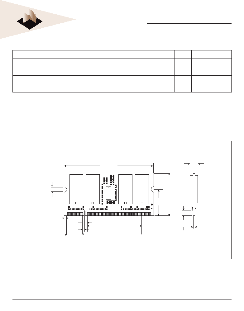
PACKAGE DIMENSIONS FOR BD4
* ALL DIMENSIONS ARE IN MILIMETERS AND (INCHES)
67.56
(2.666) MAX
0.99 ± 0.10
(0.039 ± 0.004)
6.35
(0.250) MAX.
2.31
(0.091) REF.
4.19
(0.165)
1.80
(0.071)
3.99
(0.157) MIN.
47.40
(1.866)
11.40
(0.449)
31.75
(1.25)
3.98 ± 0.1
(0.157 ± 0.004)
20
(0.787)
ORDERING INFORMATION FOR BD4
Part Number
Speed
CAS Latency
t
RCD
t
RP
Height*
W3EG72128S335BD4-xG
166MHz/333Mb/s
2.5
3
3
31.75 (1.25")
W3EG72128S262BD4-xG
133MHz/266Mb/s
2
2
2
31.75 (1.25")
W3EG72128S265BD4-xG
133MHz/266Mb/s
2.5
3
3
31.75 (1.25")
W3EG72128S202BD4-xG
100MHz/200Mb/s
2
2
2
31.75 (1.25")
NOTES:
∑ Consult Factory for availability of RoHS compliant products. (G = RoHS Compliant)
∑ Vendor specifi c part numbers are used to provide memory components source control. The place holder for this is shown as lower case "-x" in the part numbers above and is to
be replaced with the respective vendors code. Consult factory for qualifi ed sourcing options. (M = Micron, S = Samsung & consult factory for others)
∑ Consult factory for availability of industrial temperature (-40∞C to 85∞C) option
12
White Electronic Designs Corporation ∑ (602) 437-1520 ∑ www.wedc.com
White Electronic Designs
W3EG72128S-AD4
-BD4
August 2005
Rev. 3
PRELIMINARY
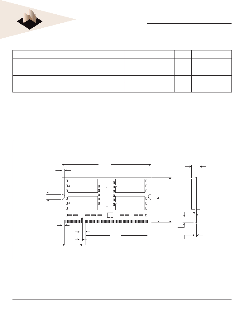
PACKAGE DIMENSIONS FOR AD4
* ALL DIMENSIONS ARE IN MILIMETERS AND (INCHES)
35.05
(1.138) MAX.
2.31
(0.091) REF.
2.0
(0.079)
67.56
(2.666) MAX.
4.19
(0.165)
1.80
(0.071)
20
(0.787)
47.40
(1.866)
11.40
(0.449)
P1
3.98 ± 0.1
(0.157 ± 0.004)
0.99 ± 0.10
(0.039 ± 0.004)
6.35
(0.250) MAX.
3.99
(0.157) MIN.
ORDERING INFORMATION FOR AD4
Part Number
Speed
CAS Latency
t
RCD
t
RP
Height*
W3EG72128S335AD4-xG
166MHz/333Mb/s
2.5
3
3
35.05 (1.138")
W3EG72128S262AD4-xG
133MHz/266Mb/s
2
2
2
35.05 (1.138")
W3EG72128S265AD4-xG
133MHz/266Mb/s
2.5
3
3
35.05 (1.138")
W3EG72128S202AD4-xG
100MHz/200Mb/s
2
2
2
35.05 (1.138")
NOTES:
∑ Consult Factory for availability of RoHS compliant products. (G = RoHS Compliant)
∑ Vendor specifi c part numbers are used to provide memory components source control. The place holder for this is shown as lower case "-x" in the part numbers above and is to
be replaced with the respective vendors code. Consult factory for qualifi ed sourcing options. (M = Micron, S = Samsung & consult factory for others)
∑ Consult factory for availability of industrial temperature (-40∞C to 85∞C) option

13
White Electronic Designs Corporation ∑ (602) 437-1520 ∑ www.wedc.com
White Electronic Designs
W3EG72128S-AD4
-BD4
August 2005
Rev. 3
PRELIMINARY
PART NUMBERING GUIDE
W 3 E G 72 128 S xxx D4 x -x G
WEDC
MEMORY
DDR
GOLD
BUS WIDTH
DEPTH
2.5V
SPEED (MHz)
PACKAGE 200 PIN
I = INDUSTRIAL
COMPONENT VENDOR NAME
(M = Micron)
(S = Samsung)
G = RoHS COMPLIANT

14
White Electronic Designs Corporation ∑ (602) 437-1520 ∑ www.wedc.com
White Electronic Designs
W3EG72128S-AD4
-BD4
August 2005
Rev. 3
PRELIMINARY
Document Title
1GB ≠ 2x64Mx72 DDR SDRAM UNBUFFERED ECC w/PLL
Revision History
Rev #
History
Release Date
Status
Rev 0
Created
7-23-03
Advanced
Rev 1
Added AD4 and BD4 package height option
4-6-04
Preliminary
Rev 2
Added AC specs
10-4-04
Preliminary
Rev 3
3.1 Added part number matrix
8-05
Preliminary