 | –≠–ª–µ–∫—Ç—Ä–æ–Ω–Ω—ã–π –∫–æ–º–ø–æ–Ω–µ–Ω—Ç: W78M64V | –°–∫–∞—á–∞—Ç—å:  PDF PDF  ZIP ZIP |

1
White Electronic Designs Corporation ∑ (602) 437-1520 ∑ www.wedc.com
White Electronic Designs
W78M64V-XSBX
December 2005
Rev. 3
White Electronic Designs Corp. reserves the right to change products or specifi cations without notice.
8Mx64 Flash 3.3V Page Mode Simultaneous Read/Write
Operation Multi-Chip Package
Access Times of 70, 90, 100, 120ns
Packaging
∑ 159 PBGA, 13x22mm ≠ 1.27mm pitch
1,000,000 Erase/Program Cycles per sector
Page Mode
∑ Page size is 8 words: Fast page read access from
random locations within the page.
Sector Architecture
∑ Bank A (16Mb): 4Kw x 8 and 32 Kw x 31
∑ Bank B (48Mb): 32Kw x 96
∑ Bank C (48Mb): 32Kw x 96
∑ Bank D (16Mb): 4Kw x 8 and 3Kw x 31
Both top and bottom boot blocks
Zero Power Operation
Organized as 8Mx64, user confi gurable as 2x8Mx32
or 4x8Mx16
Commercial, Industrial and Military Temperature
Ranges
3.3 Volt for read, erase and write operations
Simultaneous read/write operations:
∑ Data can be continuously read from one bank
while executing erase/program functions in
another bank
∑ Zero latency between read and write operations
Erase Suspend/Resume
∑ Suspends erase operations to allow read or
programming in other sectors of same bank
Data Polling and Toggle Bits
∑ Provides a software method of detecting the status
of program or erase cycles
Unlock Bypass Program command
∑ Reduces overall programming time when issuing
multiple program command sequences
Ready/Busy# output (RY/BY#)
∑ Hardware method for detecting program or erase
cycle completion
Hardware reset pin (RESET#)
∑ Hardware method of resetting the internal state
machine to the read mode
WP#/ACC input pin
∑ Write protect (WP#) function allows protection of
two outermost boot sector, regardless of sector
protect status
∑ Acceleration (ACC) function accelerates program
timing
Persistent Sector Protection
∑ A command sector protection method of locking
combinations of individual sectors and sector
groups to prevent program or erase operation
within that sector
Password Sector Protection or Cancellation
∑ A sector protection method to lock combinations
of individual sectors and sector groups to prevent
program or erase operations within that sector
using a user-defi ned 64-bit password.
* This product is subject to change without notice.
FEATURES
2
White Electronic Designs Corporation ∑ (602) 437-1520 ∑ www.wedc.com
White Electronic Designs
W78M64V-XSBX
December 2005
Rev. 3
White Electronic Designs Corp. reserves the right to change products or specifi cations without notice.
WE1#
WE2#
WE3#
WE4#
CS4#
CS3#
CS2#
CS1#
RY/BY#
RESET#
OE#
A
0-22
WP#/ACC
DQ
16-31
DQ
32-47
DQ
48-63
DQ
0-15
8M X 16
8M X 16
8M X 16
8M X 16
V
IO
V
IO
V
CC
GND
GND
GND
GND
GND
GND
V
IO
V
CC
V
IO
V
CC
V
IO
GND
GND
DQ33
DQ40
DQ32
CS
3
#
OE#
A2
A3
A4
DQ
17
DQ24
DQ16
CS2#
V
CC
GND
GND
DQ41
DQ43
DQ35
DQ42
DQ34
A0
WP#/A
CC
A6
A17
WE
2
#
DQ19
DQ26
DQ18
DQ25
GND
GND
WE
3
#
DQ45
DQ37
DQ44
DQ36
A22
A11
A9
RY/BY#
DQ29
DQ21
DQ28
DQ20
DQ27
GND
V
CC
V
CC
V
CC
V
IO
V
IO
DQ47
DQ39
DQ46
DQ38
V
CC
GND
V
CC
GND
DNU*
DQ31
DQ23
DQ30
DQ22
V
IO
DQ
57
DQ49
DQ56
DQ48
CS
4
#
A12
V
IO
GND
A14
DQ9
DQ1
DQ8
DQ0
CS
1
#
V
CC
GND
DNU
DQ59
DQ51
DQ58
DQ50
A16
A7
A1
A5
DQ4
DQ11
DQ3
DQ10
DQ2
GND
GND
WE
4
#
DQ61
DQ53
DQ60
DQ52
A21
A10
RESET#
A18
WE
1
#
DQ6
DQ13
DQ5
DQ12
GND
GND
V
CC
DQ63
DQ55
DQ62
DQ54
A20
A15
A13
A8
A19
DQ15
DQ7
DQ14
GND
GND
V
IO
V
CC
V
IO
V
CC
GND
GND
GND*
GND
GND
GND
V
IO
V
CC
V
IO
V
CC
V
IO
A
B
C
D
E
F
G
H
J
K
L
M
N
P
R
T
1
2
3
4
5
6
7
8
9 10
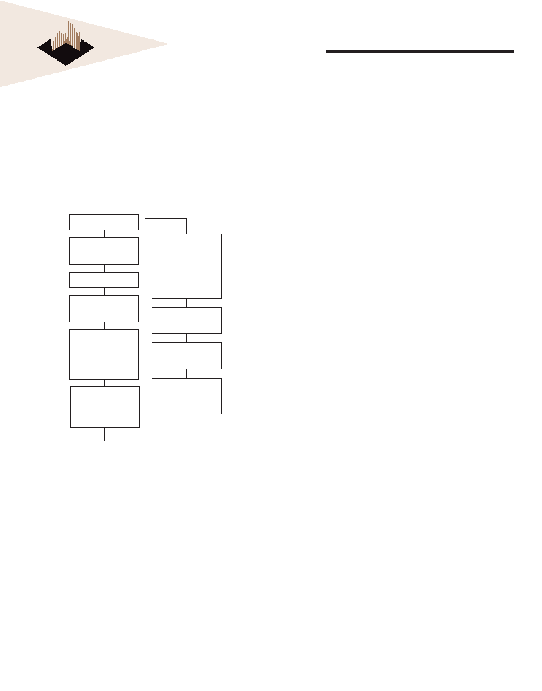
BLOCK DIAGRAM
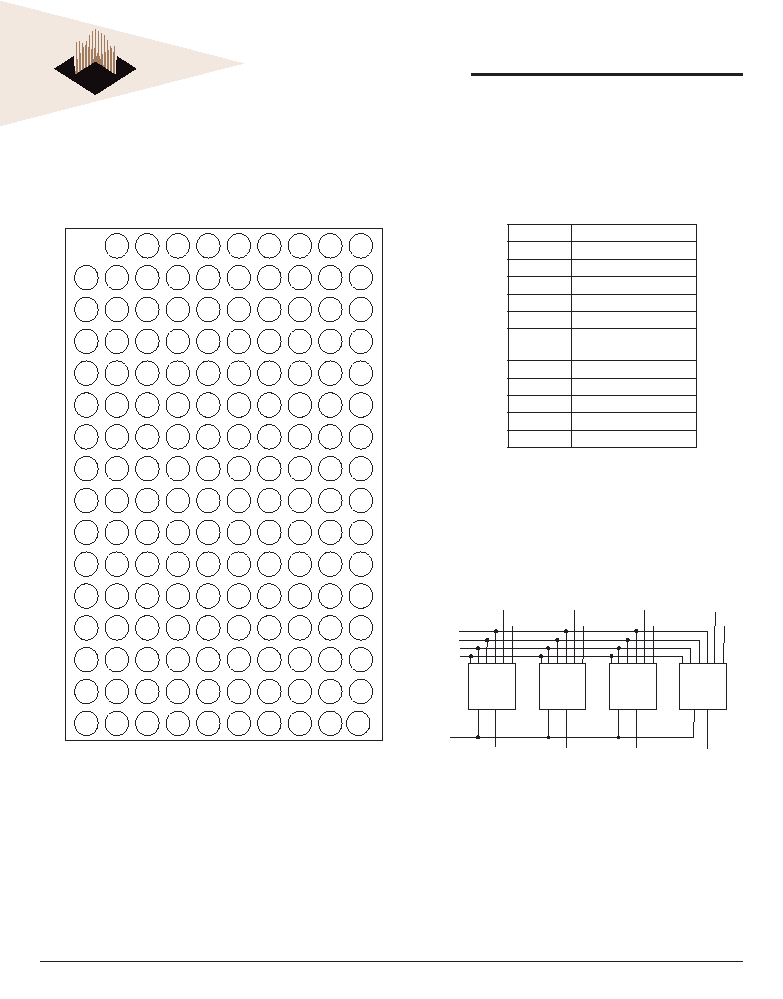
PIN DESCRIPTION
DQ
0-63
Data Inputs/Outputs
A
0-22
Address Inputs
WE#
1-4
Write Enables
CS#
1-4
Chip Selects
OE#
Output Enable
RESET#
Hardware Reset
WP#/ACC
Hardware Write
Protection/Acceleration
RY/BY#
Ready/Busy Output
V
CC
Power Supply
V
IO
I/O Power Supply
GND
Ground
DNU
Do Not Use
FIG 1: PIN CONFIGURATION
FOR W78M64V-XSBX (TOP VIEW)
* Ball L5 is reserved for A23 for future upgrades.

3
White Electronic Designs Corporation ∑ (602) 437-1520 ∑ www.wedc.com
White Electronic Designs
W78M64V-XSBX
December 2005
Rev. 3
White Electronic Designs Corp. reserves the right to change products or specifi cations without notice.
GENERAL DESCRIPTION
The W78M64V-XSBX is a 512Mb, 3.3 volt-only Page Mode
and Simultaneous Read/Write Flash memory device.
The device offers fast page access times allowing high
speed microprocessors to operate without wait states.
To eliminate bus contention the device has separate chip
enable (CS#), write enable (WE#) and output enable (OE#)
controls. Simultaneous Read/Write Operation with Zero
Latency.
The Simultaneous Read/Write architecture provides
simultaneous operation by dividing the memory space
into 4 banks, which can be considered to be four separate
memory arrays as far as certain operations are concerned.
The device can improve overall system performance by
allowing a host system to program or erase in one bank,
then immediately and simultaneously read from another
bank with zero latency (with two simultaneous operations
operating at any one time). This releases the system from
waiting for the completion of a program or erase operation,
greatly improving system performance.
The device can be organized in both top and bottom sector
confi gurations. The banks are organized as follows:
JEDEC 42.4 single-power-supply Flash standard.
Commands are written to the command register using
standard microprocessor write timing. Register contents
serve as inputs to an internal state-machine that controls the
erase and programming circuitry. Write cycles also internally
latch addresses and data needed for the programming and
erase operations. Reading data out of the device is similar
to reading from other Flash or EPROM devices.
Device programming occurs by executing the program
command sequence. The Unlock Bypass mode facilitates
faster programming times by requiring only two write cycles
to program data instead of four. Device erasure occurs by
executing the erase command sequence.
The host system can detect whether a program or erase
operation is complete by reading the DQ7 (Data# Polling)
and DQ6 (toggle) status bits. After a program or erase cycle
has been completed, the device is ready to read array data
or accept another command.
The sector erase architecture allows memory sectors to
be erased and reprogrammed without affecting the data
contents of other sectors.
Hardware data protection measures include a low
V
CC
detector that automatically inhibits write operations
during power transitions. The hardware sector protection
feature disables both program and erase operations in any
combination of sectors of memory. This can be achieved
in-system or via programming equipment.
The Erase Suspend/Erase Resume feature enables the
user to put erase on hold for any period of time to read data
from, or program data to, any sector that is not selected for
erasure. True background erase can thus be achieved. If
a read is needed from the SecSi Sector area (One Time
Program area) after an erase suspend, then the user must
use the proper command sequence to enter and exit this
region.
The device offers two power-saving features. When
addresses have been stable for a specifi ed amount of time,
the device enters the automatic sleep mode. The system
can also place the device into the standby mode. Power
consumption is greatly reduced in both these modes.
Bank Sectors
A
16 Mbit (4 Kw x 8 and 32 Kw x 31)
B
48 Mbit (32 Kw x 96)
C
48 Mbit (32 Kw x 96)
D
16 Mbit (4 Kw x 8 and 32 Kw x 31)
Page Mode Features
The page size is 8 words. After initial page access is
accomplished, the page mode operation provides fast read
access speed of random locations within that page.
Standard Flash Memory
Features
The device requires a 3.3 volt power supply for both read and
write functions. Internally generated and regulated voltages
are provided for the program and erase operations.
The device is entirely command set compatible with the
4
White Electronic Designs Corporation ∑ (602) 437-1520 ∑ www.wedc.com
White Electronic Designs
W78M64V-XSBX
December 2005
Rev. 3
White Electronic Designs Corp. reserves the right to change products or specifi cations without notice.
DEVICE BUS OPERATIONS
This section describes the requirements and use of the
device bus operations, which are initiated through the
internal command register. The command register itself
does not occupy any addressable memory location. The
register is a latch used to store the commands, along with
the address and data information needed to execute the
command. The contents of the register serve as inputs
to the internal state machine. The state machine outputs
dictate the function of the device.
Table 1
lists the device
bus operations, the inputs and control levels they require,
and the resulting output. The following subsections describe
each of these operations in further detail.
TABLE 1. DEVICE BUS OPERATION
3
Operation
CS#
OE#
WE#
RESET#
WP#/ACC
Addresses
(A22-A0)
DQ15-DQ0
Read
L
L
H
H
X
A
IN
D
OUT
Write
L
H
L
H
X
A
IN
D
IN
Standby
V
IO
±
0.3 V
X
X
V
IO
±
0.3 V
X (Note 2)
X
High-Z
Output Disable
L
H
H
H
X
X
High-Z
Reset
X
X
X
L
X
X
High-Z
Temporary Sector Unprotect (High
Voltage
X
X
X
V
ID
X
A
IN
D
IN
Legend: L = Logic Low = V
IL
, H = Logic High = V
IH,
V
ID
= 11.5-12.5 V, V
HH
= 8.5-9.5 V, X = Don't Care, SA = Sector Address, A
IN
= Address In, D
IN
= Data In,
D
OUT
= Data Out
Notes:
1.
The sector protect and sector unprotect functions may also be Implemented via programming equipment. See the High Voltage Sector Protection section.
2.
WP#/ACC must be high when writing to sectors 0, 1, 268, or 269.
3.
For each chip
REQUIREMENTS FOR READING
ARRAY DATA
To read array data from the outputs, the system must drive
the OE# and appropriate CS# pins to V
IL
. CS# is the power
control. OE# is the output control and gates array data to
the output pins. WE# should remain at V
IH.
The internal state machine is set for reading array data upon
device power-up, or after a hardware reset. This ensures
that no spurious alteration of the memory content occurs
during the power transition. No command is necessary in
this mode to obtain array data. Standard microprocessor
read cycles that assert valid addresses on the device
address inputs produce valid data on the device data
outputs. Each bank remains enabled for read access until
the command register contents are altered.
Refer to the
AC Characteristics
table for timing specifi cations
and to Figure 11 for the timing diagram. I
CC1
in the
DC Characteristics table represents the active current
specifi cation for reading array data.
Random Read (Non-Page Read)
Address access time (t
ACC
) is equal to the delay from stable
addresses to valid output data. The chip enable access
time (t
CS
) is the delay from the stable addresses and stable
CS# to valid data at the output inputs. The output enable
access time is the delay from the falling edge of the OE#
to valid data at the output inputs (assuming the addresses
have been stable for at least t
ACC
≠t
OE
time).
Page Mode Read
The device is capable of fast page mode read and is
compatible with the page mode Mask ROM read operation.
This mode provides faster read access speed for random
locations within a page. Address bits A22≠A3 select an 8
word page, and address bits A2≠A0 select a specifi c word
within that page. This is an asynchronous operation with the
microprocessor supplying the specifi c word location.
The random or initial page access is t
ACC
or t
CS
and
subsequent page read accesses (as long as the locations
specifi ed by the microprocessor falls within that page) is

5
White Electronic Designs Corporation ∑ (602) 437-1520 ∑ www.wedc.com
White Electronic Designs
W78M64V-XSBX
December 2005
Rev. 3
White Electronic Designs Corp. reserves the right to change products or specifi cations without notice.
equivalent to t
PACC
. When CS# is deasserted (CS#=V
IH
),
the reassertion of CS# for subsequent access has access
time of t
ACC
or t
CS
. Here again, CS# selects the device and
OE# is the output control and should be used to gate data
to the output inputs if the device is selected. Fast page
mode accesses are obtained by keeping A22≠A3 constant
and changing A2≠A0 to select the specifi c word within that
page.
The device features an Unlock Bypass mode to facilitate
faster programming. Once a bank enters the Unlock Bypass
mode, only two write cycles are required to program a word,
instead of four. The "Word Program Command Sequence"
section has details on programming data to the device using
both standard and Unlock Bypass command sequences.
An erase operation can erase one sector, multiple sectors,
or the entire device.
Table 4
indicates the address space
that each sector occupies. A "bank address" is the address
bits required to uniquely select a bank. Similarly, a "sector
address" refers to the address bits required to uniquely
select a sector. The "Command Defi nitions" section has
details on erasing a sector or the entire chip, or suspending/
resuming the erase operation.
I
CC2
in the DC Characteristics table represents the
active current specifi cation for the write mode. The
AC
Characteristics
section contains timing specifi cation tables
and timing diagrams for write operations.
Accelerated Program Operation
The device offers accelerated program operations through
the A
CC
function. This function is primarily intended to allow
faster manufacturing throughput at the factory.
If the system asserts V
HH
on this pin, the device automatically
enters the mentioned Unlock Bypass mode, temporarily
unprotects any protected sectors, and uses the higher
voltage on the pin to reduce the time required for program
operations. The system would use a two-cycle program
command sequence as required by the Unlock Bypass
mode. Removing V
HH
from the WP#/ACC pin returns the
device to normal operation. Note that V
HH
must not be
asserted on WP#/ACC for operations other than accelerated
programming, or device damage may result. In addition,
the WP#/ACC pin should be raised to V
CC
when not in
use. That is, the WP#/ACC pin should not be left fl oating
or unconnected; inconsistent behavior of the device may
result.
Autoselect Functions
If the system writes the autoselect command sequence, the
device enters the autoselect mode. The system can then
read autoselect codes from the internal register (which is
separate from the memory array) on DQ63≠DQ0. Standard
read cycle timings apply in this mode. Refer to the
Autoselect
Mode
and
Autoselect Command Sequence
sections for
more information.
TABLE 2. PAGE SELECT
Word
A2
A1
A0
Word 0
0
0
0
Word 1
0
0
1
Word 2
0
1
0
Word 3
0
1
1
Word 4
1
0
0
Word 5
1
0
1
Word 6
1
1
0
Word 7
1
1
1
SIMULTANEOUS OPERATION
In addition to the conventional features (read, program,
erase-suspend read, and erase-suspend program), the
device is capable of reading data from one bank of memory
while a program or erase operation is in progress in another
bank of memory (simultaneous operation). The bank can be
selected by bank addresses (A22≠A20) with zero latency.
The simultaneous operation can execute multi-function
mode in the same bank.
TABLE 3. BANK SELECT
Bank
A22-A20
Bank A
000
Bank B
001, 010, 011
Bank C
100, 101, 110
Bank D
111
WRITING COMMANDS/COMMAND
SEQUENCES
To write a command or command sequence (which includes
programming data to the device and erasing sectors of
memory), the system must drive WE# and CS# to V
IL
, and
OE# to V
IH
.

6
White Electronic Designs Corporation ∑ (602) 437-1520 ∑ www.wedc.com
White Electronic Designs
W78M64V-XSBX
December 2005
Rev. 3
White Electronic Designs Corp. reserves the right to change products or specifi cations without notice.
STANDBY MODE
When the system is not reading or writing to the device, it
can place the device in the standby mode. In this mode,
current consumption is greatly reduced, and the outputs are
placed in the high impedance state, independent of the OE#
input. The device enters the CMOS standby mode when the
CS# and RESET# pins are both held at V
IO
± 0.3 V. If CS#
and RESET# are held at V
IH
, but not within V
IO
± 0.3 V, the
device will be in the standby mode, but the standby current
will be greater. The device requires standard access time
(t
CS
) for read access when the device is in either of these
standby modes, before it is ready to read data.
If the device is deselected during erasure or programming,
the device draws active current until the operation is
completed.
I
CC3
in the
DC Characteristics
table represents the CMOS
standby current specifi cation.
AUTOMATIC SLEEP MODE
The automatic sleep mode minimizes Flash device energy
consumption. The device automatically enables this mode
when addresses remain stable for t
ACC
+ 150 ns. The
automatic sleep mode is independent of the CS#, WE#,
and OE# control signals. Standard address access timings
provide new data when addresses are changed. While in
sleep mode, output data is latched and always available
to the system. Note that during automatic sleep mode,
OE# must be at V
IH
before the device reduces current
to the stated sleep mode specifi cation. I
CC
5 in the
DC
Characteristics
table represents the automatic sleep mode
current specifi cation.
RESET#: HARDWARE RESET PIN
The RESET# pin provides a hardware method of resetting
the device to reading array data. When the RESET# pin is
driven low for at least a period of t
RP
, the device immediately
terminates any operation in progress, tristates all output
pins, and ignores all read/write commands for the duration
of the RESET# pulse. The device also resets the internal
state machine to reading array data. The operation that
was interrupted should be reinitiated once the device is
ready to accept another command sequence, to ensure
data integrity.
Current is reduced for the duration of the RESET# pulse.
When RESET# is held at V
SS
±0.3 V, the device draws
CMOS standby current (I
CC
4). If RESET# is held at V
IL
but
not within V
SS
±0.3 V, the standby current will be greater.
The RESET# pin may be tied to the system reset circuitry.
A system reset would thus also reset the Flash memory,
enabling the system to read the boot-up fi rmware from the
Flash memory.
If RESET# is asserted during a program or erase operation,
the RY/BY# pin remains a "0" (busy) until the internal reset
operation is complete, which requires a time of t
READY
(during
Embedded Algorithms). The system can thus monitor RY/
BY# to determine whether the reset operation is complete.
If RESET# is asserted when a program or erase operation
is not executing (RY/BY# pin is "1"), the reset operation is
completed within a time of t
READY
(not during Embedded
Algorithms). The system can read data t
RH
after the RESET#
pin returns to V
IH
.
Refer to the
AC Characteristic
tables for RESET# parameters
and to Figure 14 for the timing diagram.
OUTPUT DISABLE MODE
When the OE# input is at V
IH
, output from the device is
disabled. The output pins (except for RY/BY#) are placed
in the highest Impedance state.

7
White Electronic Designs Corporation ∑ (602) 437-1520 ∑ www.wedc.com
White Electronic Designs
W78M64V-XSBX
December 2005
Rev. 3
White Electronic Designs Corp. reserves the right to change products or specifi cations without notice.
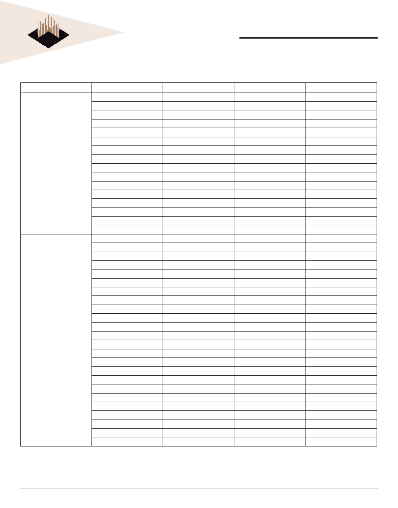
Bank
Sector
Sector Address (A22-A12)
Sector Size (Kwords)
Address Range (x16)
Bank A
SA0
00000000000
4
000000h-000FFFh
SA1
00000000001
4
001000h-001FFFh
SA2
00000000010
4
002000h-002FFFh
SA3
00000000011
4
003000h-003FFFh
SA4
00000000100
4
004000h-004FFFh
SA5
00000000101
4
005000h-005FFFh
SA6
00000000110
4
006000h-006FFFh
SA7
00000000111
4
007000h-007FFFh
SA8
00000001XXX
32
008000h-00FFFFh
SA9
00000010XXX
32
010000h-017FFFh
SA10
00000011XXX
32
018000h-01FFFFh
SA11
00000100XXX
32
020000h-027FFFh
SA12
00000101XXX
32
028000h-02FFFFh
SA13
00000110XXX
32
030000h-037FFFh
SA14
00000111XXX
32
038000h-03FFFFh
SA15
00001000XXX
32
040000h-047FFFh
SA16
00001001XXX
32
048000h-04FFFFh
SA17
00001010XXX
32
050000h-057FFFh
SA18
00001011XXX
32
058000h-05FFFFh
SA19
00001100XXX
32
060000h-067FFFh
SA20
00001101XXX
32
068000h-06FFFFh
SA21
00001110XXX
32
070000h-077FFFh
SA22
00001111XXX
32
078000h-07FFFFh
SA23
00010000XXX
32
080000h-087FFFh
SA24
00010001XXX
32
088000h-08FFFFh
SA25
00010010XXX
32
090000h-097FFFh
SA26
00010011XXX
32
098000h-09FFFFh
SA27
00010100XXX
32
0A0000h-0A7FFFh
SA28
00010101XXX
32
0A8000h-0AFFFFh
SA29
00010110XXX
32
0B0000h-0B7FFFh
SA30
00010111XXX
32
0B8000h-0BFFFFh
SA31
00011000XXX
32
0C0000h-0C7FFFh
SA32
00011001XXX
32
0C8000h-0CFFFFh
SA33
00011010XXX
32
0D0000h-0D7FFFh
SA34
00011011XXX
32
0D8000h-0DFFFFh
SA35
00011100XXX
32
0E0000h-0E7FFFh
SA36
00011101XXX
32
0E8000h-0EFFFFh
SA37
00011110XXX
32
0F0000h-0F7FFFh
SA38
00011111XXX
32
0F8000h-0FFFFFh
TABLE 4. SECTOR ARCHITECTURE

8
White Electronic Designs Corporation ∑ (602) 437-1520 ∑ www.wedc.com
White Electronic Designs
W78M64V-XSBX
December 2005
Rev. 3
White Electronic Designs Corp. reserves the right to change products or specifi cations without notice.
Bank
Sector
Sector Address (A22-A12)
Sector Size (Kwords)
Address Range (x16)
Bank B
SA39 00100000XXX 32
100000h≠107FFFh
SA40 00100001XXX 32
108000h≠10FFFFh
SA41
00100010XXX
32
110000h≠117FFFh
SA42 00100011XXX 32
118000h≠11FFFFh
SA43 00100100XXX 32
120000h≠127FFFh
SA44 00100101XXX 32
128000h≠12FFFFh
SA45 00100110XXX
32
130000h≠137FFFh
SA46
00100111XXX
32 138000h≠13FFFFh
SA47 00101000XXX 32
140000h≠147FFFh
SA48 00101001XXX 32
148000h≠14FFFFh
SA49 00101010XXX 32
150000h≠157FFFh
SA50 00101011XXX 32
158000h≠15FFFFh
SA51 00101100XXX 32
160000h≠167FFFh
SA52 00101101XXX 32
168000h≠16FFFFh
SA53 00101110XXX 32
170000h≠177FFFh
SA54 00101111XXX 32
178000h≠17FFFFh
SA55 00110000XXX 32
180000h≠187FFFh
SA56 00110001XXX 32
188000h≠18FFFFh
SA57 00110010XXX 32
190000h≠197FFFh
SA58 00110011XXX 32
198000h≠19FFFFh
SA59 00110100XXX 32
1A0000h≠1A7FFFh
SA60 00110101XXX 32
1A8000h≠1AFFFFh
SA61 00110110XXX 32
1B0000h≠1B7FFFh
SA62 00110111XXX 32
1B8000h≠1BFFFFh
SA63 00111000XXX 32
1C0000h≠1C7FFFh
SA64 00111001XXX 32
1C8000h≠1CFFFFh
SA65 00111010XXX 32
1D0000h≠1D7FFFh
SA66 00111011XXX 32
1D8000h≠1DFFFFh
SA67 00111100XXX 32
1E0000h≠1E7FFFh
SA68 00111101XXX 32
1E8000h≠1EFFFFh
SA69 00111110XXX 32
1F0000h≠1F7FFFh
SA70 00111111XXX 32
1F8000h≠1FFFFFh
SA71 01000000XXX 32
200000h≠207FFFh
SA72 01000001XXX 32
208000h≠20FFFFh
SA73 01000010XXX 32
210000h≠217FFFh
SA74 01000011XXX 32
218000h≠21FFFFh
SA75 01000100XXX 32
220000h≠227FFFh
SA76 01000101XXX 32
228000h≠22FFFFh
SA77 01000110XXX 32
230000h≠237FFFh
SA78 01000111XXX 32
238000h≠23FFFFh
TABLE 4. SECTOR ARCHITECTURE

9
White Electronic Designs Corporation ∑ (602) 437-1520 ∑ www.wedc.com
White Electronic Designs
W78M64V-XSBX
December 2005
Rev. 3
White Electronic Designs Corp. reserves the right to change products or specifi cations without notice.
Bank
Sector
Sector Address (A22-A12)
Sector Size (Kwords)
Address Range (x16)
Bank B
SA79 01001000XXX 32
240000h≠247FFFh
SA80 01001001XXX 32
248000h≠24FFFFh
SA81 01001010XXX 32
250000h≠257FFFh
SA82 01001011XXX 32
258000h≠25FFFFh
SA83
01001100XXX
32
260000h≠267FFFh
SA84 01001101XXX 32
268000h≠26FFFFh
SA85 01001110XXX 32
270000h≠277FFFh
SA86 01001111XXX 32
278000h≠27FFFFh
SA87 01010000XXX 32
280000h≠287FFFh
SA88 01010001XXX 32
288000h≠28FFFFh
SA89 01010010XXX 32
290000h≠297FFFh
SA90 01010011XXX 32
298000h≠29FFFFh
SA91 01010100XXX 32
2A0000h≠2A7FFFh
SA92 01010101XXX 32
2A8000h≠2AFFFFh
SA93 01010110XXX 32
2B0000h≠2B7FFFh
SA94 01010111XXX 32
2B8000h≠2BFFFFh
SA95 01011000XXX 32
2C0000h≠2C7FFFh
SA96 01011001XXX 32
2C8000h≠2CFFFFh
SA97 01011010XXX 32
2D0000h≠2D7FFFh
SA98 01011011XXX 32
2D8000h≠2DFFFFh
SA99 01011100XXX 32
2E0000h≠2E7FFFh
SA100 01011101XXX 32
2E8000h≠2EFFFFh
SA101 01011110XXX 32
2F0000h≠2F7FFFh
SA102 01011111XXX 32
2F8000h≠2FFFFFh
SA103 01100000XXX 32
300000h≠307FFFh
SA104 01100001XXX 32
308000h≠30FFFFh
SA105 01100010XXX 32
310000h≠317FFFh
SA106 01100011XXX 32
318000h≠31FFFFh
SA107 01100100XXX 32
320000h≠327FFFh
SA108 01100101XXX 32
328000h≠32FFFFh
SA109 01100110XXX 32
330000h≠337FFFh
SA110 01100111XXX 32
338000h≠33FFFFh
SA111 01101000XXX 32
340000h≠347FFFh
SA112 01101001XXX 32
348000h≠34FFFFh
SA113 01101010XXX 32
350000h≠357FFFh
SA114 01101011XXX 32
358000h≠35FFFFh
SA115 01101100XXX 32
360000h≠367FFFh
SA116 01101101XXX 32
368000h≠36FFFFh
SA117 01101110XXX 32
370000h≠377FFFh
SA118 01101111XXX 32
378000h≠37FFFFh
TABLE 4. SECTOR ARCHITECTURE
10
White Electronic Designs Corporation ∑ (602) 437-1520 ∑ www.wedc.com
White Electronic Designs
W78M64V-XSBX
December 2005
Rev. 3
White Electronic Designs Corp. reserves the right to change products or specifi cations without notice.
TABLE 4. SECTOR ARCHITECTURE
Bank
Sector
Sector Address (A22-A12)
Sector Size (Kwords)
Address Range (x16)
Bank B
SA119 01110000XXX 32 380000h≠387FFFh
SA120 01110001XXX 32 388000h≠38FFFFh
SA121 01110010XXX 32 390000h≠397FFFh
SA122 01110011XXX 32 398000h≠39FFFFh
SA123 01110100XXX 32 3A0000h≠3A7FFFh
SA124 01110101XXX 32 3A8000h≠3AFFFFh
SA125 01110110XXX 32 3B0000h≠3B7FFFh
SA126 01110111XXX 32 3B8000h≠3BFFFFh
SA127 01111000XXX 32
3C0000h≠3C7FFFh
SA128 01111001XXX 32
3C8000h≠3CFFFFh
SA129 01111010XXX 32
3D0000h≠3D7FFFh
SA130 01111011XXX 32
3D8000h≠3DFFFFh
SA131 01111100XXX 32
3E0000h≠3E7FFFh
SA132 01111101XXX 32
3E8000h≠3EFFFFh
SA133 01111110XXX
32 3F0000h≠3F7FFFh
SA134 01111111XXX 32
3F8000h≠3FFFFFh
Bank C
SA135 10000000XXX 32 400000h≠407FFFh
SA136 10000001XXX 32 408000h≠40FFFFh
SA137 10000010XXX 32 410000h≠417FFFh
SA138 10000011XXX 32 418000h≠41FFFFh
SA139 10000100XXX 32 420000h≠427FFFh
SA140 10000101XXX 32 428000h≠42FFFFh
SA141 10000110XXX 32 430000h≠437FFFh
SA142 10000111XXX 32 438000h≠43FFFFh
SA143 10001000XXX 32 440000h≠447FFFh
SA144 10001001XXX 32 448000h≠44FFFFh
SA145 10001010XXX 32 450000h≠457FFFh
SA146 10001011XXX 32 458000h≠45FFFFh
SA147 10001100XXX 32 460000h≠467FFFh
SA148 10001101XXX 32 468000h≠46FFFFh
SA149 10001110XXX 32 470000h≠477FFFh
SA150 10001111XXX 32 478000h≠47FFFFh
SA151 10010000XXX 32 480000h≠487FFFh
SA152 10010001XXX 32 488000h≠48FFFFh
SA153 10010010XXX 32 490000h≠497FFFh
SA154 10010011XXX 32 498000h≠49FFFFh
SA155 10010100XXX 32 4A0000h≠4A7FFFh
SA156 10010101XXX 32 4A8000h≠4AFFFFh
SA157 10010110XXX 32 4B0000h≠4B7FFFh
SA158 10010111XXX 32 4B8000h≠4BFFFFh

11
White Electronic Designs Corporation ∑ (602) 437-1520 ∑ www.wedc.com
White Electronic Designs
W78M64V-XSBX
December 2005
Rev. 3
White Electronic Designs Corp. reserves the right to change products or specifi cations without notice.
TABLE 4. SECTOR ARCHITECTURE
Bank
Sector
Sector Address (A22-A12)
Sector Size (Kwords)
Address Range (x16)
Bank C
SA159 10011000XXX 32
4C0000h≠4C7FFFh
SA160 10011001XXX 32 4C8000h≠4CFFFFh
SA161 10011010XXX 32 4D0000h≠4D7FFFh
SA162 10011011XXX 32 4D8000h≠4DFFFFh
SA163 10011100XXX 32 4E0000h≠4E7FFFh
SA164 10011101XXX 32 4E8000h≠4EFFFFh
SA165 10011110XXX 32 4F0000h≠4F7FFFh
SA166 10011111XXX 32
4F8000h≠4FFFFFh
SA167 10100000XXX 32
500000h≠507FFFh
SA168 10100001XXX 32
508000h≠50FFFFh
SA169 10100010XXX 32 510000h≠517FFFh
SA170 10100011XXX 32 518000h≠51FFFFh
SA171 10100100XXX 32 520000h≠527FFFh
SA172 10100101XXX 32 528000h≠52FFFFh
SA173 10100110XXX 32
538000h≠53FFFFh
SA175 10101000XXX 32 540000h≠547FFFh
SA176
10101001XXX 32
548000h≠54FFFFh
SA177 10101010XXX 32 550000h≠557FFFh
SA178 10101011XXX 32 558000h≠15FFFFh
SA179 10101100XXX 32 560000h≠567FFFh
SA180 10101101XXX 32 568000h≠56FFFFh
SA181 10101110XXX 32 570000h≠577FFFh
SA182
10101111XXX 32
578000h≠57FFFFh
SA183 10110000XXX 32
580000h≠587FFFh
SA184 10110001XXX 32 588000h≠58FFFFh
SA185 10110010XXX 32 590000h≠597FFFh
SA186 10110011XXX 32 598000h≠59FFFFh
SA187 10110100XXX 32 5A0000h≠5A7FFFh
SA188 10110101XXX 32 5A8000h≠5AFFFFh
SA189 10110110XXX 32 5B0000h≠5B7FFFh
SA190 10110111XXX 32 5B8000h≠5BFFFFh
SA191 10111000XXX 32 5C0000h≠5C7FFFh
SA192 10111001XXX 32 5C8000h≠5CFFFFh
SA193 10111010XXX 32 5D0000h≠5D7FFFh
SA194 10111011XXX 32 5D8000h≠5DFFFFh
SA195 10111100XXX 32 5E0000h≠5E7FFFh
SA196 10111101XXX 32 5E8000h≠5EFFFFh
SA197 10111110XXX 32
5F0000h≠5F7FFFh
SA198 10111111XXX 32 5F8000h≠5FFFFFh

12
White Electronic Designs Corporation ∑ (602) 437-1520 ∑ www.wedc.com
White Electronic Designs
W78M64V-XSBX
December 2005
Rev. 3
White Electronic Designs Corp. reserves the right to change products or specifi cations without notice.
TABLE 4. SECTOR ARCHITECTURE
Bank
Sector
Sector Address (A22-A12)
Sector Size (Kwords)
Address Range (x16)
Bank C
SA199 11000000XXX 32 600000h≠607FFFh
SA200 11000001XXX 32 608000h≠60FFFFh
SA201 11000010XXX 32 610000h≠617FFFh
SA202 11000011XXX 32
618000h≠61FFFFh
SA203 11000100XXX 32
620000h≠627FFFh
SA204 11000101XXX 32
628000h≠62FFFFh
SA205 11000110XXX 32 630000h≠637FFFh
SA206 11000111XXX 32 638000h≠63FFFFh
SA208 11001001XXX 32 648000h≠64FFFFh
SA209 11001010XXX 32 650000h≠657FFFh
SA210 11001011XXX 32 658000h≠65FFFFh
SA211 11001100XXX 32 660000h≠667FFFh
SA212 11001101XXX 32 668000h≠66FFFFh
SA213 11001110XXX 32 670000h≠677FFFh
SA214 11001111XXX 32
678000h≠67FFFFh
SA215 11010000XXX 32 680000h≠687FFFh
SA216 11010001XXX 32 688000h≠68FFFFh
SA217 11010010XXX 32 690000h≠697FFFh
SA218 11010011XXX 32 698000h≠69FFFFh
SA219 11010100XXX 32 6A0000h≠6A7FFFh
SA220 11010101XXX 32 6A8000h≠6AFFFFh
SA221 11010110XXX 32 6B0000h≠6B7FFFh
SA222 11010111XXX 32 6B8000h≠6BFFFFh
SA223 11011000XXX 32 6C0000h≠6C7FFFh
SA224 11011001XXX 32 6C8000h≠6CFFFFh
SA225 11011010XXX
32 6D0000h≠6D7FFFh
SA226 11011011XXX 32 6D8000h≠6DFFFFh
SA227 11011100XXX 32 6E0000h≠6E7FFFh
SA228 11011101XXX 32 6E8000h≠6EFFFFh
SA229 11011110XXX
32 6F0000h≠6F7FFFh
SA230 11011111XXX 32
6F8000h≠6FFFFFh

13
White Electronic Designs Corporation ∑ (602) 437-1520 ∑ www.wedc.com
White Electronic Designs
W78M64V-XSBX
December 2005
Rev. 3
White Electronic Designs Corp. reserves the right to change products or specifi cations without notice.
TABLE 4. SECTOR ARCHITECTURE
Bank
Sector
Sector Address (A22-A12)
Sector Size (Kwords)
Address Range (x16)
Bank D
SA231
11100000XXX
32
700000h-707FFFh
SA232
11100001XXX
32
708000h-70FFFFh
SA233
11100010XXX
32
710000h-717FFFh
SA234
11100011XXX
32
718000h-71FFFFh
SA235
11100100XXX
32
720000h-727FFFh
SA236
11100101XXX
32
728000h-72FFFFh
SA237
11100110XXX
32
730000h-737FFFh
SA238
11100111XXX
32
738000h-73FFFFh
SA239
11101000XXX
32
740000h-747FFFh
SA240
11101001XXX
32
748000h-74FFFFh
SA241
11101010XXX
32
750000h-757FFFh
SA242
11101011XXX
32
758000h-75FFFFh
SA243
11101100XXX
32
760000h-767FFFh
SA244
11101101XXX
32
768000h-76FFFFh
SA245
11101110XXX
32
770000h-777FFFh
SA246
11101111XXX
32
778000h-77FFFFh
SA247
11110000XXX
32
780000h-787FFFh
SA248
11110001XXX
32
788000h-78FFFFh
SA249
11110010XXX
32
790000h-797FFFh
SA250
11110011XXX
32
798000h-79FFFFh
SA251
11110100XXX
32
7A0000h-7A7FFFh
SA252
11110101XXX
32
7A8000h-7AFFFFh
SA253
11110110XXX
32
7B0000h-7B7FFFh
SA254
11110111XXX
32
7B8000h-7BFFFFh
SA255
11111000XXX
32
7O0000h-7C7FFFh
SA256
11111001XXX
32
7C8000h-7CFFFFh
SA257
11111010XXX
32
7D0000h-7D7FFFh
SA258
11111011XXX
32
7D8000h-7DFFFFh
SA259
11111100XXX
32
7E0000h-7E7FFFh
SA260
11111101XXX
32
7E8000h-7EFFFFh
SA261
11111110XXX
32
7F0000h-7F7FFFh
SA262
11111111000
4
7F8000h-7F8FFFh
SA263
11111111001
4
7F9000h-7F9FFFh
SA264
11111111010
4
7FA000h-7FAFFFh
SA265
11111111011
4
7FB000h-7FBFFFh
SA266
11111111100
4
7FO000h-7FCFFFh
SA267
11111111101
4
7FD000h-7FDFFFh
SA268
11111111110
4
7FE000h-7FEFFFh
SA269
11111111111
4
7FF000h-7FFFFFh

14
White Electronic Designs Corporation ∑ (602) 437-1520 ∑ www.wedc.com
White Electronic Designs
W78M64V-XSBX
December 2005
Rev. 3
White Electronic Designs Corp. reserves the right to change products or specifi cations without notice.
TABLE 5.
SecSi
TM
SECTOR ADDRESSES
Sector Size
Address Range
Device
128 words
000000h≠00007Fh
Factory-Locked Area
64 words
000000h-00003Fh
Customer-Lockable Area
64 words
000040h-00007Fh
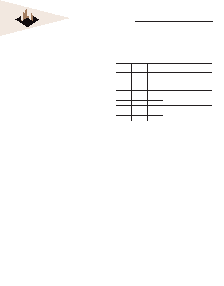
AUTOSELECT MODE
The autoselect mode provides manufacturer and device
identifi cation, and sector protection verifi cation, through
identifi er codes output on DQ7≠DQ0 for each chip. This
mode is primarily intended for programming equipment
to automatically match a device to be programmed with
its corresponding programming algorithm. However, the
autoselect codes can also be accessed in-system through
the command register.
When using programming equipment, the autoselect
mode requires V
ID
on address pin A9. Address pins
must be as shown in
Table 6
. In addition, when verifying
sector protection, the sector address must appear on
the appropriate highest order address bits (see
Table
4
).
Table 6
shows the remaining address bits that are
don't care. When all necessary bits have been set as
required, the programming equipment may then read the
corresponding identifi er code on DQ7≠DQ0. However, the
autoselect codes can also be accessed in-system through
the command register, for instances when the device is
erased or programmed in a system without access to high
voltage on the A9 pin. The command sequence is illustrated
in
Table 13
. Note that if a Bank Address (BA) on address
bits A22≠A20 is asserted during the third write cycle of the
autoselect command, the host system can read autoselect
data that bank and then immediately read array data from
the other bank, without exiting the autoselect mode.
To access the autoselect codes in-system, the host system
can issue the autoselect command via the command
register, as shown in
Table 13
. This method does not require
V
ID
. Refer to the
Autoselect Command Sequence
section
for more information.
TABLE 6. AUTOSELECT CODES (HIGH VOLTAGE METHOD)
Description
CS#
OE#
WE#
A22
to
A12
A10
A9
A8
A7
A6
A5
to
A4
A3
A2
A1
A0
DQ15
to
DQ0 (each chip)
Manufacturer ID:
L
L
H
X
X
V
ID
X
L
L
X
L
L
L
L
0004h
Device ID
Read
Cycle 1
L
L
H
X
X
V
ID
X
L
L
L
L
L
L
H
227Eh
Read
Cycle 2
L
H
H
H
L
2220
Read
Cycle 3
L
H
H
H
H
2200h
Sector Protection
Verifi cation
L
L
H
SA
X
V
ID
X
L
L
L
L
L
H
L
0001h (protected),
0000h (unprotected)
SecSi Indicator Bit
(DQ7, DQ6)
L
L
H
X
X
V
ID
X
X
L
X
L
L
H
H
00C0h (factory and
user locked)
Legend: L = Logic Low = V
IL
, H = Logic High = V
IH
, BA = Bank Address, SA = Sector Address, X = Don't care. Note: The autoselect codes may also be accessed in-system
via command sequences

15
White Electronic Designs Corporation ∑ (602) 437-1520 ∑ www.wedc.com
White Electronic Designs
W78M64V-XSBX
December 2005
Rev. 3
White Electronic Designs Corp. reserves the right to change products or specifi cations without notice.
TABLE 7. BOOT SECTOR/SECTOR
BLOCK ADDRESSES FOR PROTECTION/
UNPROTECTION
Sector A22-A12
Sector/
Sector Block Size
SA0 00000000000
4
Kwords
SA1 00000000001
4
Kwords
SA2 00000000010
4
Kwords
SA3 00000000011
4
Kwords
SA4 00000000100
4
Kwords
SA5 00000000101
4
Kwords
SA6 00000000110
4
Kwords
SA7 00000000111
4
Kwords
SA8-SA10
00000001XXX
00000010XXX
00000011XXX
96 (3x32) Kwords
SA11-SA14
000001XXXXX
128 (4x32) Kwords
SA15-SA18
000010XXXXX
128 (4x32) Kwords
SA19-SA22
000011XXXXX
128 (4x32) Kwords
SA23-SA26
000100XXXXX
128 (4x32) Kwords
SA27-SA30
000101XXXXX
128 (4x32) Kwords
SA31-SA34
000110XXXXX
128 (4x32) Kwords
SA35-SA38
000111XXXXX
128 (4x32) Kwords
SA39-SA42
001000XXXXX
128 (4x32) Kwords
SA43-SA46
001001XXXXX
128 (4x32) Kwords
SA47-SA50
001010XXXXX
128 (4x32) Kwords
SA51-SA54
001011XXXXX
128 (4x32) Kwords
SA55-SA58
001100XXXXX
128 (4x32) Kwords
SA59-SA62
001101XXXXX
128 (4x32) Kwords
SA63-SA66
001110XXXXX
128 (4x32) Kwords
SA67-SA70 001111XXXXX
128 (4x32) Kwords
SA71-SA74
010000XXXXX
128 (4x32) Kwords
SA75-SA78
010001XXXXX
128 (4x32) Kwords
SA79-SA82
010010XXXXX
128 (4x32) Kwords
SA83-SA86
010011XXXXX
128 (4x32) Kwords
SA87-SA90
010100XXXXX
128 (4x32) Kwords
SA91-SA94
010101XXXXX
128 (4x32) Kwords
SA95-SA98
010110XXXXX
128 (4x32) Kwords
SA99-SA102
010111XXXXX
128 (4x32) Kwords
SA103-SA106
011000XXXXX
128 (4x32) Kwords
SA107-SA110
011001XXXXX
128 (4x32) Kwords
SA111-SA114
011010XXXXX
128 (4x32) Kwords
SA115-SA118
011011XXXXX
128 (4x32) Kwords
SA119-SA122
011100XXXXX
128 (4x32) Kwords
SA123-SA126
011101XXXXX
128 (4x32) Kwords
SA127-SA130 011110XXXXX
128 (4x32) Kwords
Sector
A22-A12
Sector/
Sector Block Size
SA131-SA134 011111XXXXX
128 (4x32) Kwords
SA135-SA138
100000XXXXX
128 (4x32) Kwords
SA139-SA142
100001XXXXX
128 (4x32) Kwords
SA143-SA146
100010XXXXX
128 (4x32) Kwords
SA147-SA150
100011XXXXX
128 (4x32) Kwords
SA151-SA154
100100XXXXX
128 (4x32) Kwords
SA155-SA158
100101XXXXX
128 (4x32) Kwords
SA159-SA162
100110XXXXX
128 (4x32) Kwords
SA163-SA166
100111XXXXX
128 (4x32) Kwords
SA167-SA170
101000XXXXX
128 (4x32) Kwords
SA171-SA174
101001XXXXX
128 (4x32) Kwords
SA175-SA178
101010XXXXX
128 (4x32) Kwords
SA179-SA182
101011XXXXX
128 (4x32) Kwords
SA183-SA186
101100XXXXX
128 (4x32) Kwords
SA187-SA190
101101XXXXX
128 (4x32) Kwords
SA191-SA194
101110XXXXX
128 (4x32) Kwords
SA195-SA198
101111XXXXX
128 (4x32) Kwords
SA199-SA202
110000XXXXX
128 (4x32) Kwords
SA203-SA206
110001XXXXX
128 (4x32) Kwords
SA207-SA210
110010XXXXX
128 (4x32) Kwords
SA211-SA214
110011XXXXX
128 (4x32) Kwords
SA215-SA218
110100XXXXX
128 (4x32) Kwords
SA219-SA222
110101XXXXX
128 (4x32) Kwords
SA223-SA226
110110XXXXX
128 (4x32) Kwords
SA227-SA230
110111XXXXX
128 (4x32) Kwords
SA231-SA234
111000XXXXX
128 (4x32) Kwords
SA235-SA238
111001XXXXX
128 (4x32) Kwords
SA239-SA242
111010XXXXX
128 (4x32) Kwords
SA243-SA246
111011XXXXX
128 (4x32) Kwords
SA247-SA250
111100XXXXX
128 (4x32) Kwords
SA251-SA254
111101XXXXX
128 (4x32) Kwords
SA255-SA258
111110XXXXX
128 (4x32) Kwords
SA259-SA261
11111100XXX
11111101XXX
11111110XXX
96 (3x32) Kwords
SA262
11111111000 4
Kwords
SA263
11111111001 4
Kwords
SA264
11111111010 4
Kwords
SA265
11111111011 4
Kwords
SA266
11111111100 4
Kwords
SA267
11111111101 4
Kwords
SA268
11111111110 4
Kwords
SA269
11111111111 4
Kwords

16
White Electronic Designs Corporation ∑ (602) 437-1520 ∑ www.wedc.com
White Electronic Designs
W78M64V-XSBX
December 2005
Rev. 3
White Electronic Designs Corp. reserves the right to change products or specifi cations without notice.
SECTOR PROTECTION
The device features several levels of sector protection,
which can disable both the program and erase operations
in certain sectors or sector groups:
Persistent Sector Protection
A command sector protection method that replaces the old
12 V controlled protection method.
Password Sector Protection
A highly sophisticated protection method that requires
a password before changes to certain sectors or sector
groups are permitted
WP# Hardware Protection
A write protect pin that can prevent program or erase
operations in sectors 0, 1, 268, and 269.
The WP# Hardware Protection feature is always available,
independent of the software managed protection method
chosen.
Selecting a Sector Protection Mode
All parts default to operate in the Persistent Sector
Protection mode. The user must then choose if the
Persistent or Password Protection method is most desirable.
There are two one-time programmable non-volatile bits
that defi ne which sector protection method will be used.
If the Persistent Sector Protection method is desired,
programming the Persistent Sector Protection Mode
Locking Bit permanently sets the device to the Persistent
Sector Protection mode. If the Password Sector Protection
method is desired, programming the Password Mode
Locking Bit permanently sets the device to the Password
Sector Protection mode. It is not possible to switch between
the two protection modes once a locking bit has been set.
One of the two modes must be selected when the device
is fi rst programmed. This prevents a program or virus from
later setting the Password Mode Locking Bit, which would
cause an unexpected shift from the default Persistent Sector
Protection Mode into the Password Protection Mode.
The device is shipped with all sectors unprotected.
It is possible to determine whether a sector is protected or
unprotected. See
Autoselect Mode
for details.
PERSISTENT SECTOR PROTECTION
The Persistent Sector Protection method replaces the 12
V controlled protection method in previous WEDC fl ash
devices. This new method provides three different sector
protection states:
Persistently Locked--The sector is protected and
cannot be changed.
Dynamically Locked--The sector is protected and
can be changed by a simple command.
Unlocked--The sector is unprotected and can be
changed by a simple command.
To achieve these states, three types of "bits" are used:
Persistent Protection Bit (PPB)
A single Persistent (non-volatile) Protection Bit is assigned
to a maximum four sectors (see the sector address tables
for specifi c sector protection groupings). All 4 Kword boot-
block sectors have individual sector Persistent Protection
Bits (PPBs) for greater fl exibility. Each PPB is individually
modifi able through the PPB Write Command.
The device erases all PPBs in parallel. If any PPB requires
erasure, the device must be instructed to preprogram all
of the sector PPBs prior to PPB erasure. Otherwise, a
previously erased sector PPBs can potentially be over-
erased. The fl ash device does not have a built-in means
of preventing sector PPBs over-erasure.
Persistent Protection Bit Lock (PPB Lock)
The Persistent Protection Bit Lock (PPB Lock) is a global
volatile bit. When set to "1", the PPBs cannot be changed.
When cleared ("0"), the PPBs are changeable. There is
only one PPB Lock bit per device. The PPB Lock is cleared
after power-up or hardware reset. There is no command
sequence to unlock the PPB Lock.
Dynamic Protection Bit (DYB)
A volatile protection bit is assigned for each sector. After
power-up or hardware reset, the contents of all DYBs is
"0". Each DYB is individually modifi able through the DYB
Write Command.
When the parts are fi rst shipped, the PPBs are cleared, the
DYBs are cleared, and PPB Lock is defaulted to power up in
the cleared state ≠ meaning the PPBs are changeable.
When the device is fi rst powered on the DYBs power up
cleared (sectors not protected). The Protection State for
each sector is determined by the logical OR of the PPB and
the DYB related to that sector. For the sectors that have the
PPBs cleared, the DYBs control whether or not the sector
is protected or unprotected. By issuing the DYB Write
17
White Electronic Designs Corporation ∑ (602) 437-1520 ∑ www.wedc.com
White Electronic Designs
W78M64V-XSBX
December 2005
Rev. 3
White Electronic Designs Corp. reserves the right to change products or specifi cations without notice.
command sequences, the DYBs will be set or cleared, thus
placing each sector in the protected or unprotected state.
These are the so-called Dynamic Locked or Unlocked
states. They are called dynamic states because it is very
easy to switch back and forth between the protected and
unprotected conditions. This allows software to easily protect
sectors against inadvertent changes yet does not prevent
the easy removal of protection when changes are needed.
The DYBs maybe set or cleared as often as needed.
The PPBs allow for a more static, and diffi cult to change,
level of protection. The PPBs retain their state across power
cycles because they are non-volatile. Individual PPBs are set
with a command but must all be cleared as a group through
a complex sequence of program and erasing commands.
The PPBs are also limited to 100 erase cycles.
The PPB Lock bit adds an additional level of protection.
Once all PPBs are programmed to the desired settings, the
PPB Lock may be set to "1". Setting the PPB Lock disables
all program and erase commands to the non-volatile PPBs.
In effect, the PPB Lock Bit locks the PPBs into their current
state. The only way to clear the PPB Lock is to go through
a power cycle. System boot code can determine if any
changes to the PPB are needed; for example, to allow new
system code to be downloaded. If no changes are needed
then the boot code can set the PPB Lock to disable any
further changes to the PPBs during system operation.
The WP#/ACC write protect pin adds a final level of
hardware protection to sectors 0, 1, 268, and 269. When
this pin is low it is not possible to change the contents of
these sectors. These sectors generally hold system boot
code. The WP#/ACC pin can prevent any changes to the
boot code that could override the choices made while setting
up sector protection during system initialization.
It is possible to have sectors that have been persistently
locked, and sectors that are left in the dynamic state. The
sectors in the dynamic state are all unprotected. If there
is a need to protect some of them, a simple DYB Write
command sequence is all that is necessary. The DYB write
command for the dynamic sectors switch the DYBs to signify
protected and unprotected, respectively. If there is a need to
change the status of the persistently locked sectors, a few
more steps are required. First, the PPB Lock bit must be
disabled by either putting the device through a power-cycle,
or hardware reset. The PPBs can then be changed to refl ect
the desired settings. Setting the PPB lock bit once again will
lock the PPBs, and the device operates normally again.
The best protection is achieved by executing the PPB lock
bit set command early in the boot code, and protect the boot
code by holding WP#/ACC = V
IL
.
TABLE 8. SECTOR PROTECTION SCHEMES
DYB
PPB
PPB
LOCK
SECTOR STATE
0
0
0
Unprotected - PPB and DYB are
changeable
0
0
1
Unprotected - PPB not changeable,
DYB is changeable
0
1
0
Protected - PPB and DYB are
changeable
1
0
0
1
1
0
0
1
1
Protected - PPB not changeable,
DYB is changeable
1
0
1
1
1
1
Table 8 contains all possible combinations of the DYB, PPB,
and PPB lock relating to the status of the sector
In summary, if the PPB is set, and the PPB lock is set, the
sector is protected and the protection can not be removed
until the next power cycle clears the PPB lock. If the PPB is
cleared, the sector can be dynamically locked or unlocked.
The DYB then controls whether or not the sector is protected
or unprotected.
If the user attempts to program or erase a protected sector,
the device ignores the command and returns to read mode.
A program command to a protected sector enables status
polling for approximately 1 µs beforethe device returns to
read mode without having modifi ed the contents of the
protected sector. An erase command to a protected sector
enables status polling for approximately 50 µs after which
the device returns to read mode without having erased the
protected sector.
The programming of the DYB, PPB, and PPB lock for a
given sect or can be ver i f ied by writing a DYB/PPB/PPB
lock verify command to the device.
Persistent Sector Protection Mode Locking Bit
Like the password mode locking bit, a Persistent Sector
Protection mode locking bit exists to guarantee that the
device remain in software sector protection. Once set,
the Persistent Sector Protection locking bit prevents
programming of the password protection mode locking bit.
This guarantees that a hacker could not place the device
in password protection mode.

18
White Electronic Designs Corporation ∑ (602) 437-1520 ∑ www.wedc.com
White Electronic Designs
W78M64V-XSBX
December 2005
Rev. 3
White Electronic Designs Corp. reserves the right to change products or specifi cations without notice.
PASSWORD PROTECTION MODE
The Password Sector Protection Mode method allows an
even higher level of security than the Persistent Sector
Protection Mode. There are two main differences between
the Persistent Sector Protection and the Password Sector
Protection Mode:
When the device is fi rst powered on, or comes out
of a reset cycle, the PPB Lock bit set to the locked
state, rather than cleared to the unlocked state.
The only means to clear the PPB Lock bit is by
writing a unique 64-bit Password to the device.
The Password Sector Protection method is otherwise
identical to the Persistent Sector Protection method.
A 64-bit password is the only additional tool utilized in this
method.
Once the Password Mode Locking Bit is set, the password
is permanently set with no means to read, program, or erase
it. The password is used to clear the PPB Lock bit. The
Password Unlock command must be written to the fl ash,
along with a password. The fl ash device internally compares
the given password with the pre-programmed password.
If they match, the PPB Lock bit is cleared, and the PPBs
can be altered. If they do not match, the fl ash device does
nothing. There is a built-in 2 µs delay for each "password
check." This delay is intended to thwart any efforts to run
a program that tries all possible combinations in order to
crack the password.
Password and Password Mode Locking Bit
In order to select the Password sector protection scheme,
the customer must first program the password. The
password may be correlated to the unique Electronic
Serial Number (ESN) of the particular fl ash device. Each
ESN is different for every fl ash device; therefore each
password should be different for every fl ash device. While
programming in the password region, the customer may
perform Password Verify operations.
Once the desired password is programmed in, the customer
must then set the Password Mode Locking Bit. This
operation achieves two objectives:
1. Permanently sets the device to operate using the
Password Protection Mode. It is not possible to reverse
this function.
2. Disables all further commands to the password region.
All program, and read operations are ignored.
Both of these objectives are important, and if not carefully
considered, may lead to unrecoverable errors. The user
must be sure that the Password Protection method is
desired when setting the Password Mode Locking Bit. More
importantly, the user must be sure that the password is
correct when the Password Mode Locking Bit is set. Due to
the fact that read operations are disabled, there is no means
to verify what the password is afterwards. If the password
is lost after setting the Password Mode Locking Bit, there
will be no way to clear the PPB Lock bit.
The Password Mode Locking Bit, once set, prevents reading
the 64-bit password on the DQ bus and further password
programming. The Password Mode Locking Bit is not
erasable. Once Password Mode Locking Bit is programmed,
the Persistent Sector Protection Locking Bit is disabled
from programming, guaranteeing that no changes to the
protection scheme are allowed.
64-bit Password
The 64-bit Password is located in its own memory space and
is accessible through the use of the Password Program and
Verify commands (see "Password Verify Command"). The
password function works in conjunction with the Password
Mode Locking Bit, which when set, prevents the Password
Verify command from reading the contents of the password
on the pins of the device.
WRITE PROTECT (WP#)
The Write Protect feature provides a hardware method of
protecting sectors 0, 1, 268, and 269 without using V
ID
.
This function is provided by the WP# pin and overrides
the previously discussed
High Voltage Sector Protection
method.
If the system asserts V
IL
on the WP#/ACC pin, the device
disables program and erase functions in the two outermost
4 Kword sectors on both ends of the fl ash array independent
of whether it was previously protected or unprotected.
If the system asserts V
IH
on the WP#/ACC pin, the device
reverts to whether sectors 0, 1, 268, and 269 were last set
to be protected or unprotected. That is, sector protection
or unprotection for these sectors depends on whether
they were last protected or unprotected using the method
described in
High Voltage Sector Protection
.
Note that the WP#/ACC pin must not be left fl oating or
unconnected; inconsistent behavior of the device may
result.

19
White Electronic Designs Corporation ∑ (602) 437-1520 ∑ www.wedc.com
White Electronic Designs
W78M64V-XSBX
December 2005
Rev. 3
White Electronic Designs Corp. reserves the right to change products or specifi cations without notice.
Persistent Protection Bit Lock
The Persistent Protection Bit (PPB) Lock is a volatile bit that
refl ects the state of the Password Mode Locking Bit after
power-up reset. If the Password Mode Lock Bit is also set
after a hardware reset (RESET# asserted) or a power-up
reset, the ONLY means for clearing the PPB Lock Bit in
Password Protection Mode is to issue the Password Unlock
command. Successful execution of the Password Unlock
command clears the PPB Lock Bit, allowing for sector PPBs
modifi cations. Asserting RESET#, taking the device through
a power-on reset, or issuing the PPB Lock Bit Set command
sets the PPB Lock Bit to a "1" when the Password Mode
Lock Bit is not set.
If the Password Mode Locking Bit is not set, including
Persistent Protection Mode, the PPB Lock Bit is cleared
after power-up or hardware reset. The PPB Lock Bit is set
by issuing the PPB Lock Bit Set command. Once set the only
means for clearing the PPB Lock Bit is by issuing a hardware
or power-up reset. The Password Unlock command is
ignored in Persistent Protection Mode.
HIGH VOLTAGE SECTOR PROTECTION
Sector protection and unprotection may also be implemented
using programming equipment. The procedure requires
high voltage (V
ID
) to be placed on the RESET# pin. Refer
to
Figure 2
for details on this procedure. Note that for sector
unprotect, all unprotected sectors must fi rst be protected
prior to the fi rst sector write cycle.

20
White Electronic Designs Corporation ∑ (602) 437-1520 ∑ www.wedc.com
White Electronic Designs
W78M64V-XSBX
December 2005
Rev. 3
White Electronic Designs Corp. reserves the right to change products or specifi cations without notice.
Sector Protect:
Write 60h to sector
address with
A7-A0 =
00000010
Set up sector
address
Wait 100 µs
Verify Sector
Protect: Write 40h
to sector address
with A7-A0 =
00000010
Read from
sector address
with A7-A0 =
00000010
START
PLSCNT = 1
RESET# = V
ID
Wait 4 µs
First Write
Cycle = 60h?
Data = 01h?
Remove V
ID
from RESET#
Write reset
command
Sector Protect
complete
Yes
Yes
No
PLSCNT
= 25?
Yes
Device failed
Increment
PLSCNT
Temporary Sector
Unprotect Mode
No
Sector Unprotect:
Write 60h to sector
address with
A7-A0 =
01000010
Set up first sector
address
Wait 1.2 ms
Verify Sector
Unprotect: Write
40h to sector
address with
A7-A0 =
00000010
Read from
sector address
with A7-A0 =
00000010
START
PLSCNT = 1
RESET# = V
ID
Wait 4 µs
Data = 00h?
Last sector
verified?
Remove V
ID
from RESET#
Write reset
command
Sector Unprotect
complete
Yes
No
PLSCNT
= 1000?
Yes
Device failed
Increment
PLSCNT
Temporary Sector
Unprotect Mode
No
All sectors
protected?
Yes
Protect all sectors:
The indicated portion
of the sector protect
algorithm must be
performed for all
unprotected sectors
prior to issuing the
first sector
unprotect address
Set up
next sector
address
No
Yes
No
Yes
No
No
Yes
No
Sector Protect
Algorithm
Sector Unprotect
Algorithm
First Write
Cycle = 60h?
Protect another
sector?
Reset
PLSCNT = 1
Remove V
ID
from RESET#
Write reset
command
Sector Protect
complete
Remove V
ID
from RESET#
Write reset
command
Sector Unprotect
complete
FIGURE 2. IN-SYSTEM SECTOR PROTECTION/SECTOR UNPROTECTION ALGORITHMS

21
White Electronic Designs Corporation ∑ (602) 437-1520 ∑ www.wedc.com
White Electronic Designs
W78M64V-XSBX
December 2005
Rev. 3
White Electronic Designs Corp. reserves the right to change products or specifi cations without notice.
TEMPORARY SECTOR UNPROTECT
This feature allows temporary unprotection of previously
protected sectors to change data in-system. The Sector
Unprotect mode is activated by setting the RESET# pin to
V
ID
. During this mode, formerly protected sectors can be
programmed or erased by selecting the sector addresses.
Once V
ID
is removed from the RESET# pin, all the previously
protected sectors are protected again. Figure 3 shows the
algorithm, and Figure 24 shows the timing diagrams, for
this feature. While PPB lock is set, the device cannot enter
the Temporary Sector Unprotection Mode.
SecSi sector is divided into 64 factory-lockable words that
can be programmed and locked by the user. The SecSi
sector is located at addresses 000000h-00007Fh in both
Persistent Protection mode and Password Protection mode.
It uses indicator bits (DQ6, DQ7) to indicate the factory-
locked and user-locked status of the part.
The system accesses the SecSi Sector through a command
sequence (see "Enter SecSiTM Sector/Exit SecSi Sector
Command Sequence"). After the sysem has written the
Enter SecSi Sector command sequence, it may read the
SecSi Sector by using the addresses normally occupied by
the boot sectors. This mode of operation continues until the
system issues the Exit SecSi Sector command sequence,
or until power is removed from the device. On power-up, or
following a hardware reset, the device reverts to sending
commands to the normal address space. Note that the ACC
function and unlock bypass modes are not available when
the SecSi Sector is enabled.
Factory-Locked Area (64 words)
The factory-locked area of the SecSi Sector (000000h-
00003Fh) is locked when the part is shipped, whether or
not the area was programmed at the factory. The SecSi
Sector Factory-locked Indicator Bit (DQ7) is permanently
set to a "1".
User-Lockable Area (64 words)
The user-lockable area of the SecSi Sector (000040h-
00007Eh) is shipped unprotected, which allows the user
to program and optionally lock the area as appropriate for
the application. The SecSi Sector User-locked Indicator Bit
(DQ6) is shipped as "0" and can be permanently locked to
"1" by issuing the SecSi Protection Bit Program Command.
The SecSi Sector can be read any number of times, but
can be programmed and locked only once. Note that
the accelerated programming (ACC) and unlock bypass
functions are not available when programming the SecSi
Sector.
The User-lockable SecSi Sector area can be protected using
one of the following procedures:
Follow the SecSi Sector protection Agorithm as
shown in Figure 4. This allows in-system protection
of the SecSi Sector without raising any device pin
to a high voltage. Note that this method is only
appliacable to the SecSi Sector.
To verify the protect/unprotect status of the SecSi
Sector, follow the algorithm shown in
Figure 5
.
SecSiTM (SECURED SILICON) SECTOR
FLASH MEMORY REGION
The SecSi (Secured Silicon) Sector feature provides a Flash
memory region that enables permanent part identifi cation
through an Electronic Serial Number (ESN) The 128-word
START
Perform Erase or
Program Operations
RESET# = V
IH
Temporary Sector
Unprotect Completed
(Note 2)
RESET# = V
ID
(Note 1)
FIGURE 3. TEMPORARY SECTOR UNPROTECT
OPERATION
Notes:
1. All protected sectors unprotected (If WP#/ACC = VIL, sectors 0, 1, 268, 269 will
remain protected).
2. All previously protected sectors are protected once again

22
White Electronic Designs Corporation ∑ (602) 437-1520 ∑ www.wedc.com
White Electronic Designs
W78M64V-XSBX
December 2005
Rev. 3
White Electronic Designs Corp. reserves the right to change products or specifi cations without notice.
START
SecSi
Sector Entry
Write AAh to address 555h
Write 55h to address 2AAh
Write 88h to a address 555h
TM
SecSi Sector
Protection Entry
Write AAh to address 555h
Write 55h to address 2AAh
Write 60h to a address 555h
PLSCNT = 1
Protect SecSi Sector:
write 68h to sector address
with A7-A0 = 00011010
Time out 256 µs
Verify SecSi Sector:
write 48h to sector address
with A7-A0 = 00011010
Read from sector address
with A7-A0 = 00011010
Increment PLSCNT
SecSi Sector Entry
SecSi Sector Protection
No
No
Device Failed
Data = 01h?
Yes
Yes
SecSi Sector
Protection Completed
SecSi Sector Exit
Write 555h/AAh
Write 2AAh/55Ah
Write SA0+555h/90h
Write XXXh/00h
SecSi Secto r Exit
PLSCNT = 25?
FIGURE 4. SECSI SECTOR PROTECTION ALGORITHM
23
White Electronic Designs Corporation ∑ (602) 437-1520 ∑ www.wedc.com
White Electronic Designs
W78M64V-XSBX
December 2005
Rev. 3
White Electronic Designs Corp. reserves the right to change products or specifi cations without notice.
Once the SecSi Sector is locked and verifi ed, the system
must write the Exit SecSi Sector Region command
sequence to return to reading and writing the remainder
of the array.
The SecSi Sector lock must be used with caution since,
once locked, there is no procedure available for unlocking
the SecSi Sector area and none of the bits in the SecSi
Sector memory space can be modifi ed in any way.
program/erase circuits are disabled, and the device resets
to the read mode. Subsequent writes are ignored until V
CC
is greater than V
LKO
. The system must provide the proper
signals to the control pins to prevent unintentional writes
when V
CC
is greater than V
LKO
.
Write Pulse "Glitch" Protection
Noise pulses of less than 3 ns (typical) on OE#, CS#, or
WE# do not initiate a write cycle.
Logical Inhibit
Write cycles are inhibited by holding any one of OE# = V
IL
,
CS# = V
IH
or WE# = V
IH
. To initiate a write cycle, CS# and
WE# must be a logical zero while OE# is a logical one.
Power-Up Write Inhibit
If WE# = CS# = V
IL
and OE# = V
IH
during power up, the
device does not accept commands on the rising edge of
WE#. The internal state machine is automatically reset to
the read mode on power-up.
COMMON FLASH MEMORY
INTERFACE (CFI)
The Common Flash Interface (CFI) specifi cation outlines
device and host system software interrogation handshake,
which allows specifi c vendor-specifi ed software algorithms
to be used for entire families of devices. Software support
can then be device-independent, JEDEC ID-independent,
and forward- and backward-compatible for the specifi ed
fl ash device families. Flash vendors can standardize their
existing interfaces for long-term compatibility.
This device enters the CFI Query mode when the system
writes the CFI Query command, 98h, to address 55h, any
time the device is ready to read array data. The system
can read CFI information at the addresses given in Tables
9
≠
12
. To terminate reading CFI data, the system must write
the reset command. The CFI Query mode is not accessible
when the device is executing an Embedded Program or
embedded Erase algorithm.
The system can also write the CFI query command when
the device is in the autoselect mode. The device enters the
CFI query mode, and the system can read CFI data at the
addresses given in Tables
9
≠
12
. The system must write the
reset command to return the device to reading array data.
Write 60h to
any address
Write 40h to SecSi
Sector address
with A6 = 0,
A1 = 1, A0 = 0
RESET# =
V
IH
or V
ID
Wait 1 µs
Read from SecSi
Sector address
with A6 = 0,
A1 = 1, A0 = 0
If data = 00h,
SecSi Sector is
unprotected.
If data = 01h,
SecSi Sector is
protected.
Remove V
IH
or V
ID
from RESET#
Write reset
command
SecSi Sector
Protect Verify
complete
START
SecSi Sector Protection Bits
The SecSi Sector Protection Bits prevent programming of
the SecSi Sector memory area. Once set, the SecSi Sector
memory area contents are non-modifi able.
Hardware Data Protection
The command sequence requirement of unlock cycles for
programming or erasing provides data protection against
inadvertent writes. In addition, the following hardware
data protection measures prevent accidental erasure
or programming, which might otherwise be caused by
spurious system level signals during V
CC
power-up and
power-down transitions, or from system noise.
Low V
CC
Write Inhibit
When V
CC
is less than V
LKO
, the device does not accept
any write cycles. This protects data during V
CC
power-up
and power-down. The command register and all internal
FIGURE 5. SecSi SECTOR PROTECT VERIFY
24
White Electronic Designs Corporation ∑ (602) 437-1520 ∑ www.wedc.com
White Electronic Designs
W78M64V-XSBX
December 2005
Rev. 3
White Electronic Designs Corp. reserves the right to change products or specifi cations without notice.
TABLE 9. CFI QUERY IDENTIFICATION STRING
Addresses
Data
Description
10h
11h
12h
0051h
0052h
0059h
Query Unique ASCII string "QRY"
13h
14h
0002h
0000h
Primary OEM Command Set
15h
16h
0040h
0000h
Address for Primary Extended Table
17h
18h
0000h
0000h
Alternate OEM Command Set (00h = none exists)
19h
1Ah
0000h
0000h
Address for Alternate OEM Extended Table (00H = none exists)
TABLE 10. SYSTEM INTERFACE STRING
Addresses
Data
Description
1Bh
0027h
VCC Min. (write/erase)
D7-D4: volt, D3-D0: 100 millivolt
1Ch
0036h
VCC Max. (write/erase)
D7-D4: volt, D3-D0: 100 millivolt
1Dh
0000h
VPP Min. voltage (00h = no VPP pin present)
1Eh
0000h
VPP Max. voltage (00h = no VPP pin present)
1Fh
0004h
Typical timeout per single byte/word write 2
N
µs
20h
0000h
Typical timeout for Min. size buffer write 2
N
µs (00h = not supported)
21h
0009h
Typical timeout per individual block erase 2
N
ms
22h
0000h
Typical timeout for full chip erase 2
N
ms (00h = not supported)
23h
0005h
Max. timeout for byte/word write 2
N
times typical
24h
0000h
Max. timeout for buffer write 2
N
times typical
25h
0004h
Max. timeout per individual block erase 2
N
times typical
26h
0000h
Max. timeout for full chip erase 2
N
times typical (00h = not supported)

25
White Electronic Designs Corporation ∑ (602) 437-1520 ∑ www.wedc.com
White Electronic Designs
W78M64V-XSBX
December 2005
Rev. 3
White Electronic Designs Corp. reserves the right to change products or specifi cations without notice.
TABLE 11. DEVICE GEOMETRY DEFINITION
Addresses
Data
Description
27h
0018h
Device Size = 2
N
byte
28h
29h
0001h
0000h
Flash Device Interface description
2Ah
2Bh
0000h
0000h
Max. munber of byte in multi-byte write = 2
N
(00h = not supported)
2Ch
0003h
Number of Erase Block Region within device
2Dh
2Eh
2Fh
30h
0007h
0000h
0020h
0000h
Erase Block Region 1 Information
31h
32h
33h
34h
00FDh
0000h
0000h
0001h
Erase Block Region 2 information
35h
36h
37h
38h
0007h
0000h
0020h
0000h
Erase Block Region 3 Information
39h
3Ah
3Bh
3Ch
0000h
0000h
0000h
0000h
Erase Block Region 4 Information
26
White Electronic Designs Corporation ∑ (602) 437-1520 ∑ www.wedc.com
White Electronic Designs
W78M64V-XSBX
December 2005
Rev. 3
White Electronic Designs Corp. reserves the right to change products or specifi cations without notice.
TABLE 12. PRIMARY VENDOR-SPECIFIC EXTENDED QUERY
Addresses
Data
Description
40h
41h
42h
0050h
0052h
0049h
Query-unique ASCII String "PRI"
43h
0031h
Major version number, ASCII (refl ects modifi cations to the silicon)
44h
0033h
Minor version number, ASCII (refl ects modifi cations to the CFI table)
45h
000Ch
Address Sensitive Unlock (Bits 1-0)
0 = Required, 1 = Not Required
Silicon Revision Number (Bits 7-2)
46h
0002h
Erase Suspend
0 = Not Supported, 1 = To Read Only, 2 = To Read & Write
47h
0001h
Sector Protect
0 = Not Supported, X = Number of sectors in per group
48h
0001h
Sector Temporary Unprotect
00 = Not Supported, 01 = Supported
49h
0007h
Sector Protect/Unprotect scheme
01 = 29F040 mode, 02 = 29F016 mode, 03 = 29F400, 04 = 29LV800 mode
4Ah
00E7h
Simultaneous Operation
00 = Not Supported, X = Number of Sectors excluding Bank 1
4Bh
0000h
Burst Mode Type
00 = Not Supported, 01 = Supported
4Ch
0002h
Page Mode Type
00 = Not Supported, 01 = 4 Word Page, 02 = 8 Word Page
4Dh
0085h
ACC (Acceleration) Supply Minimum
00h = Not Supported, D7-D4; Volt, D3-D0: 100 mV
4Eh
0095h
ACC (Acceleration) Supply Maximum
00h = Not Supported, D7-D4; Volt, D3-D0: 100 mV
4Fh
0001h
Top/Bottom Boot Sector Flag
00h = Uniform Device, 02h = Bottom Boot Device, 03 = Top Boot Device, 04h = Both Top and
Bottom
50h
0001h
Program Suspend
0 = Not supported, 1 = Supported
57h
0004h
Bank Organization
00 = Data at 4Ah is zero, X = Number of Banks
58h
0027h
Bank 1 Region Information
X = Number of Sectors in Bank 1
59h
0060h
Bank 2 Region Information
X = Number of Sectors in Bank 2
5Ah
0060h
Bank 3 Region Information
X = Number of Sectors in Bank 3
5Bh
0027h
Bank 4 Region Information
X = Number of Sectors in Bank 4

27
White Electronic Designs Corporation ∑ (602) 437-1520 ∑ www.wedc.com
White Electronic Designs
W78M64V-XSBX
December 2005
Rev. 3
White Electronic Designs Corp. reserves the right to change products or specifi cations without notice.
COMMAND DEFINITIONS
Writing specifi c address and data commands or sequences
into the command register initiates device operations.
Table
13
defi nes the valid register command sequences. Writing
incorrect address and data values or writing them in the
improper sequence may place the device in an unknown
state. A reset command is then required to return the device
to reading array data.
All addresses are latched on the falling edge of WE# or CS#,
whichever happens later. All data is latched on the rising
edge of WE# or CS#, whichever happens fi rst. Refer to the
AC Characteristic
section for timing diagrams.
Reading Array Data
The device is automatically set to reading array data after
device power-up. No commands are required to retrieve
data. Each bank is ready to read array data after completing
an Embedded Program or Embedded Erase algorithm.
After the device accepts an Erase Suspend command, the
corresponding bank enters the erase-suspend- read mode,
after which the system can read data from any non-erase-
suspended sector within the same bank. The system can
read array data using the standard read timing, except that
if it reads at an address within erase-suspended sectors, the
device outputs status data. After completing a programming
operation in the Erase Suspend mode, the system may
once again read array data with the same exception. See
the
Erase Suspend/Erase Resume Commands
section for
more information.
The system must issue the reset command to return a bank
to the read (or erase-suspend-read) mode if DQ5 goes
high during an active program or erase operation, or if the
bank is in the autoselect mode. See the next section,
Reset
Command
, for more information.
See also
Requirements for Reading Array Data
in the
Device Bus Operations
section for more information. The
AC Characteristic
table provides the read parameters, and
Figure 11 shows the timing diagram.
Reset Command
Writing the reset command resets the banks to the read or
erase-suspend-read mode. Address bits are don't cares
for this command.
The reset command may be written between the sequence
cycles in an erase command sequence before erasing
begins. This resets the bank to which the system was writing
to the read mode. Once erasure begins, however, the device
ignores reset commands until the operation is complete.
The reset command may be written between the sequence
cycles in a program command sequence before programming
begins. This resets the bank to which the system was writing
to the read mode. If the program command sequence is
written to a bank that is in the Erase Suspend mode, writing
the reset command returns that bank to the erase-suspend-
read mode. Once programming begins, however, the device
ignores reset commands until the operation is complete.
The reset command may be written between the sequence
cycles in an autoselect command sequence. Once in the
autoselect mode, the reset command must be written to
return to the read mode. If a bank entered the autoselect
mode while in the Erase Suspend mode, writing the reset
command returns that bank to the erase-suspend-read
mode.
If DQ5 goes high during a program or erase operation,
writing the reset command returns the banks to the read
mode (or erase-suspend-read mode if that bank was in
Erase Suspend).
Autoselect Command Sequence
The autoselect command sequence allows the host
system to access the manufacturer and device codes, and
determine whether or not a sector is protected.
The autoselect command sequence may be written to an
address within a bank that is either in the read or erase-
suspend-read mode. The autoselect command may not be
written while the device is actively programming or erasing
in the other bank. The autoselect command sequence is
initiated by fi rst writing two unlock cycles. This is followed
by a third write cycle that contains the bank address and the
autoselect command. The bank then enters the autoselect
mode. The system may read any number of autoselect
codes without reinitiating the command sequence.
Table 13
shows the address and data requirements. To
determine sector protection information, the system must
write to the appropriate bank address (BA) and sector
address (SA).
Table 4
shows the address range and bank
number associated with each sector.
The system must write the reset command to return to the
read mode (or erase-suspend-read mode if the bank was
previously in Erase Suspend).
Enter SecSiTM Sector/Exit SecSi Sector Command
Sequence
The SecSi Sector region provides a secured data area
containing a random, eight word electronic serial number

28
White Electronic Designs Corporation ∑ (602) 437-1520 ∑ www.wedc.com
White Electronic Designs
W78M64V-XSBX
December 2005
Rev. 3
White Electronic Designs Corp. reserves the right to change products or specifi cations without notice.
(ESN). The system can access the SecSi Sector region
by issuing the three-cycle Enter SecSi Sector command
sequence. The device continues to access the SecSi
Sector region until the system issues the four-cycle
Exit SecSi Sector command sequence. The Exit SecSi
Sector command sequence returns the device to normal
operation. The SecSi Sector is not accessible when the
device is executing an Embedded Program or embedded
Erase algorithm.
Table 13
shows the address and data
requirements for both command sequences. See also
"SecSiTM (Secured Silicon) Sector Flash Memory Region"
for further information. Note that the ACC function and
unlock bypass modes are not available when the SecSi
Sector is enabled.
Word Program Command Sequence
Programming is a four-bus-cycle operation. The program
command sequence is initiated by writing two unlock write
cycles, followed by the program set-up command. The
program address and data are written next, which in turn
initiate the Embedded Program algorithm. The system
is not required to provide further controls or timings. The
device automatically provides internally generated program
pulses and verifi es the programmed cell margin.
Table 13
shows the address and data requirements for the program
command sequence. Note that the SecSi Sector, autoselect,
and CFI functions are unavailable when a [program/erase]
operation is in progress.
When the Embedded Program algorithm is complete, that
bank then returns to the read mode and addresses are no
longer latched. The system can determine the status of the
program operation by using DQ7, DQ6, or RY/BY#. Refer
to the
Write Operation Status
section for information on
these status bits.
Any commands written to the device during the Embedded
Program Algorithm are ignored. Note that a hardware reset
immediately terminates the program operation. The program
command sequence should be reinitiated once that bank
has returned to the read mode, to ensure data integrity.
Programming is allowed in any sequence and across sector
boundaries. A bit cannot be programmed from "0" back
to a "1." Attempting to do so may cause that bank to set
DQ5 = 1, or cause the DQ7 and DQ6 status bits to indicate
the operation was successful. However, a succeeding read
will show that the data is still "0." Only erase operations can
convert a "0" to a "1."
Unlock Bypass Command Sequence
The unlock bypass feature allows the system to program
data to a bank faster than using the standard program
command sequence. The unlock bypass command
sequence is initiated by fi rst writing two unlock cycles. This is
followed by a third write cycle containing the unlock bypass
command, 20h. That bank then enters the unlock bypass
mode. A two-cycle unlock bypass program command
sequence is all that is required to program in this mode.
The fi rst cycle in this sequence contains the unlock bypass
program command, A0h; the second cycle contains the
program address and data. Additional data is programmed
in the same manner. This mode dispenses with the initial two
unlock cycles required in the standard program command
sequence, resulting in faster total programming time.
Table
13
shows the requirements for the command sequence.
During the unlock bypass mode, only the Unlock Bypass
Program and Unlock Bypass Reset commands are valid.
To exit the unlock bypass mode, the system must issue
the two-cycle unlock bypass reset command sequence.
(See Table 14)
The device offers accelerated program operations through
the WP#/ACC pin. When the system asserts V
HH
on the
WP# ACC pin, the device automatically enters the Unlock
Bypass mode. The system may then write the two-cycle
Unlock Bypass program command sequence. The device
uses the higher voltage on the WP#/ACC pin to accelerate
the operation. Note that the WP#/ACC pin must not be at
V
HH
any operation other than accelerated programming,
or device damage may result. In addition, the WP#/ACC
pin must not be left fl oating or unconnected; inconsistent
behavior of the device may result.
Figure 6 illustrates the algorithm for the program operation.
Refer to the
Erase and Program Operations
table in the AC
Characteristics section for parameters,
and
Figure 16
for
timing diagrams.
Chip Erase Command Sequence
Chip erase is a six bus cycle operation. The chip erase
command sequence is initiated by writing two unlock cycles,
followed by a set-up command. Two additional unlock write
cycles are then followed by the chip erase command, which
in turn invokes the Embedded Erase algorithm. The device
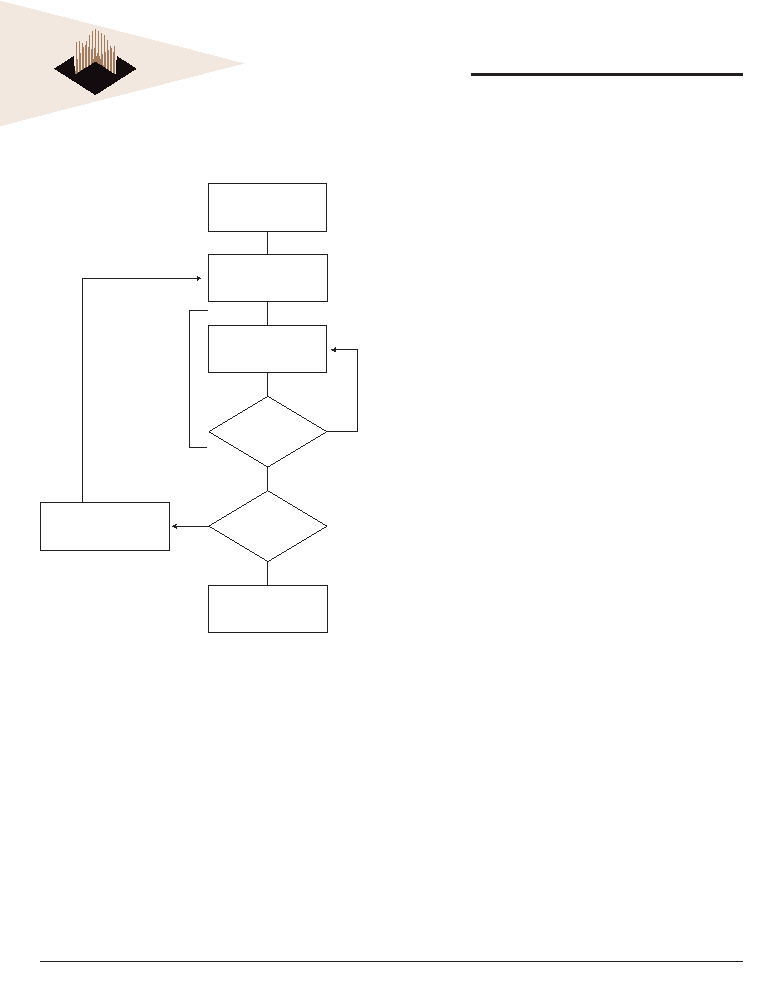
29
White Electronic Designs Corporation ∑ (602) 437-1520 ∑ www.wedc.com
White Electronic Designs
W78M64V-XSBX
December 2005
Rev. 3
White Electronic Designs Corp. reserves the right to change products or specifi cations without notice.
does not require the system to preprogram prior to erase.
The Embedded Erase algorithm automatically preprograms
and verifi es the entire memory for an all zero data pattern
prior to electrical erase. The system is not required to
provide any controls or timings during these operations.
Table 13
shows the address and data requirements for the
chip erase command sequence.
When the Embedded Erase algorithm is complete, that
bank returns to the read mode and addresses are no longer
latched. The system can determine the status of the erase
operation by using DQ7, DQ6, DQ2, or RY/BY#. Refer to
the
Write Operation Status
section for information on these
status bits.
Any commands written during the chip erase operation
are ignored. Note that SecSi Sector, autoselect, and CFI
functions are unavailable when a [program/erase] operation
is in progress. However, note that a hardware reset
immediately terminates the erase operation. If that occurs,
the chip erase command sequence should be reinitiated
once that bank has returned to reading array data, to ensure
data integrity.
Figure 7 illustrates the algorithm for the erase operation.
Refer to the
Erase and Program Operations
tables in the
AC Characteristics section for parameters, and
Figure 17
section for timing diagrams.
Sector Erase Command Sequence
Sector erase is a six bus cycle operation. The sector erase
command sequence is initiated by writing two unlock cycles,
followed by a set-up command. Two additional unlock cycles
are written, and are then followed by the address of the
sector to be erased, and the sector erase command.
Table
13
shows the address and data requirements for the sector
erase command sequence.
The device does not require the system to preprogram prior
to erase. The Embedded Erase algorithm automatically
programs and verifi es the entire memory for an all zero data
pattern prior to electrical erase. The system is not required to
provide any controls or timings during these operations.
After the command sequence is written, a sector erase time-
out of 50 µs occurs. During the time-out period, additional
sector addresses and sector erase commands may be
written. Loading the sector erase buffer may be done in any
sequence, and the number of sectors may be from one sector
to all sectors. The time between these additional cycles must
be less than 50 µs, otherwise erasure may begin. Any sector
erase address and command following the exceeded time-
out may or may not be accepted. It is recommended that
processor interrupts be disabled during this time to ensure
all commands are accepted. The interrupts can be re-
enabled after the last Sector Erase command is written. Any
command other than Sector Erase or Erase Suspend
during the time-out period resets that bank to the read
mode. The system must rewrite the command sequence
and any additional addresses and commands. Note that
SecSi Sector, autoselect, and CFI functions are unavailable
when a [program/erase] operation is in progress.
The system can monitor DQ3 to determine if the sector
erase timer has timed out (See the section on DQ3: Sector
Erase Timer). The time-out begins from the rising edge of
the fi nal WE# pulse in the command sequence.
When the Embedded Erase algorithm is complete, the bank
returns to reading array data and addresses are no longer
START
Write Program
Command Sequence
Data Poll
from System
Verify Data?
No
Yes
Last Address?
No
Yes
Programming
Completed
Increment Address
Embedded
Program
algorithm
in progress
FIGURE 6. PROGRAM OPERATION
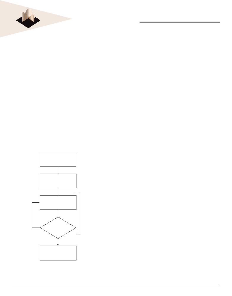
30
White Electronic Designs Corporation ∑ (602) 437-1520 ∑ www.wedc.com
White Electronic Designs
W78M64V-XSBX
December 2005
Rev. 3
White Electronic Designs Corp. reserves the right to change products or specifi cations without notice.
latched. Note that while the Embedded Erase operation is
in progress, the system can read data from the non-erasing
bank. The system can determine the status of the erase
operation by reading DQ7, DQ6, DQ2, or RY/BY# in the
erasing bank. Refer to the
Write Operation Status
section
for information on these status bits.
Once the sector erase operation has begun, only the
Erase Suspend command is valid. All other commands are
ignored. However, note that a hardware reset immediately
terminates the erase operation. If that occurs, the sector
erase command sequence should be reinitiated once that
bank has returned to reading array data, to ensure data
integrity.
Figure 7 illustrates the algorithm for the erase operation.
Refer to the
Erase and Program Operations
tables in the
AC Characteristics section for parameters, and
Figure 17
section for timing diagrams.
ERASE SUSPEND/ERASE RESUME
COMMANDS
The Erase Suspend command, B0h, allows the system to
interrupt a sector erase operation and then read data from,
or program data to, any sector not selected for erasure. The
bank address is required when writing this command. This
command is valid only during the sector erase operation,
including the 80 µs time-out period during the sector erase
command sequence.
The Erase Suspend command is ignored if written during the
chip erase operation or Embedded Program algorithm.
When the Erase Suspend command is written during the
sector erase operation, the device requires a maximum of
20 µs to suspend the erase operation. However, when the
Erase Suspend command is written during the sector erase
time-out, the device immediately terminates the time-out
period and suspends the erase operation. Addresses are
"don't-cares" when writing the Erase suspend command.
After the erase operation has been suspended, the bank
enters the erase-suspend-read mode. The system can
read data from or program data to any sector not selected
for erasure. (The device "erase suspends" all sectors
selected for erasure.) Reading at any address within
erase-suspended sectors produces status information on
DQ7≠DQ0. The system can use DQ7, or DQ6 and DQ2
together, to determine if a sector is actively erasing or is
erase-suspended. Refer to the
Write Operation Status
section for information on these status bits.
After an erase-suspended program operation is complete,
the bank returns to the erase-suspend-read mode. The
system can determine the status of the program operation
using the DQ7 or DQ6 status bits, just as in the standard
Word Program operation. Refer to the
Write Operation
Status
section for more information.
In the erase-suspend-read mode, the system can also issue
the autoselect command sequence. The device allows
reading autoselect codes even at addresses within erasing
sectors, since the codes are not stored in the memory array.
When the device exits the autoselect mode, the device
reverts to the Erase Suspend mode, and is ready for another
valid operation. Refer to the
Autoselect Mode
and
Autoselect
Command Sequence
sections for details.
To resume the sector erase operation, the system must write
the Erase Resume command (address bits are don't care).
The bank address of the erase-suspended bank is required
when writing this command. Further writes of the Resume
START
Write Erase
Command Sequence
(Notes 1, 2)
Data Poll to Erasing
Bank from System
Data = FFh?
No
Yes
Erasure Completed
Embedded
Erase
algorithm
in progress
Notes:
1. See Table 13 for erase command sequence.
2. See the section on DQ3 for information on the sector erase timer.
FIGURE 7. ERASE OPERATION

31
White Electronic Designs Corporation ∑ (602) 437-1520 ∑ www.wedc.com
White Electronic Designs
W78M64V-XSBX
December 2005
Rev. 3
White Electronic Designs Corp. reserves the right to change products or specifi cations without notice.
command are ignored. Another Erase Suspend command
can be written after the chip has resumed erasing.
PASSWORD PROGRAM COMMAND
The Password Program Command permits programming
the password that is used as part of the hardware protection
scheme. The actual password is 64-bits long. Four Password
Program commands are required to program the password.
The system must enter the unlock cycle, password program
command (38h) and the program address/data for each
portion of the password when programming. There are
no provisions for entering the 2-cycle unlock cycle, the
password program command, and all the password
data. There is no special addressing order required for
programming the password. Also, when the password
is undergoing programming, Simultaneous Operation is
disabled. Read operations to any memory location will
return the programming status. Once programming is
complete, the user must issue a Read/Reset command to
return the device to normal operation. Once the Password
is written and verifi ed, the Password Mode Locking Bit
must be set in order to prevent verifi cation. The Password
Program Command is only capable of programming "0"s.
Programming a "1" after a cell is programmed as a "0" results
in a time-out by the Embedded Program AlgorithmTM with
the cell remaining as a "0". The password is all ones when
shipped from the factory. All 64-bit password combinations
are valid as a password.
PASSWORD VERIFY COMMAND
The Password Verify Command is used to verify the
Password. The Password is verifiable only when the
Password Mode Locking Bit is not programmed. If the
Password Mode Locking Bit is programmed and the user
attempts to verify the Password, the device will always drive
all F's onto the DQ data bus.
The Password Verify command is permitted if the SecSi
sector is enabled. Also, the device will not operate in
Simultaneous Operation when the Password Verify
command is executed. Only the password is returned
regardless of the bank address. The lower two address bits
(A1-A0) are valid during the Password Verify. Writing the
Read/Reset command returns the device back to normal
operation.
PASSWORD PROTECTION MODE
LOCKING BIT PROGRAM COMMAND
The Password Protection Mode Locking Bit Program
Command programs the Password Protection Mode
Locking Bit, which prevents further verifi es or updates to
the Password. Once programmed, the Password Protection
Mode Locking Bit cannot be erased! If the password
Protection Mode Locking Bit is verifi ed as program without
margin, the Password Protection Mode Locking Bit Program
command can be executed to improve the program
margin. Once the Password Protection Mode Locking Bit is
programmed, the Persistent Sector Protection Locking Bit
program circuitry is disabled, thereby forcing the device to
remain in the Password Protection mode. Exiting the Mode
Locking Bit Program command is accomplished by writing
the Read/Reset command.
PERSISTENT SECTOR PROTECTION
MODE LOCKING BIT PROGRAM
COMMAND
The Persistent Sector Protection Mode Locking Bit Program
Command programs the Persistent Sector Protection Mode
Locking Bit, which prevents the Password Mode Locking
Bit from ever being programmed. If the Persistent Sector
Protection Mode Locking Bit is verifi ed as programmed
without margin, the Persistent Sector Protection Mode
Locking Bit Program Command should be reissued to
improve program margin. By disabling the program circuitry
of the Password Mode Locking Bit, the device is forced to
remain in the Persistent Sector Protection mode of operation,
once this bit is set. Exiting the Persistent Protection Mode
Locking Bit Program command is accomplished by writing
the Read/Reset command.
SecSi SECTOR PROTECTION BIT
PROGRAM COMMAND
The SecSi Sector Protection Bit Program Command
programs the SecSi Sector Protection Bit, which prevents
the SecSi sector memory from being cleared. If the SecSi
Sector Protection Bit is verifi ed as programmed without
margin, the SecSi Sector Protection Bit Program Command
should be reissued to improve program margin. Exiting the
V
CC
-level SecSi Sector Protection Bit Program Command is
accomplished by writing the Read/Reset command.

32
White Electronic Designs Corporation ∑ (602) 437-1520 ∑ www.wedc.com
White Electronic Designs
W78M64V-XSBX
December 2005
Rev. 3
White Electronic Designs Corp. reserves the right to change products or specifi cations without notice.
PPB LOCK BIT SET COMMAND
The PPB Lock Bit Set command is used to set the PPB
Lock bit if it is cleared either at reset or if the Password
Unlock command was successfully executed. There is no
PPB Lock Bit Clear command.
Once the PPB Lock Bit is set, it cannot be cleared unless the
device is taken through a power-on clear or the Password
Unlock command is executed. Upon setting the PPB Lock
Bit, the PPBs are latched into the DYBs. If the Password
Mode Locking Bit is set, the PPB Lock Bit status is refl ected
as set, even after a power-on reset cycle. Exiting the PPB
Lock Bit Set command is accomplished by writing the Read/
Reset command (only in the Persistent Protection Mode).
DYB WRITE COMMAND
The DYB Write command is used to set or clear a DYB for
a given sector. The high order address bits
(A22≠A12) are issued at the same time as the code 01h or
00h on DQ7-DQ0. All other DQ data bus pins are ignored
during the data write cycle. The DYBs are modifi able at
any time, regardless of the state of the PPB or PPB Lock
Bit. The DYBs are cleared at power-up or hardware reset.
Exiting the DYB Write command is accomplished by writing
the Read/Reset command.
PASSWORD UNLOCK COMMAND
The Password Unlock command is used to clear the PPB
Lock Bit so that the PPBs can be unlocked for modifi cation,
thereby allowing the PPBs to become accessible for
modifi cation. The exact password must be entered in order
for the unlocking function to occur. This command cannot
be issued any faster than 2 µs at a time to prevent a hacker
from running through all 64-bit combinations in an attempt
to correctly match a password. If the command is issued
before the 2 µs execution window for each portion of the
unlock, the command will be ignored.
Once the Password Unlock command is entered, the
RY/BY# indicates that the device is busy. Approximately 1
µs is required for each portion of the unlock. Once the fi rst
portion of the password unlock completes (RY/BY# is not
low or DQ6 does not toggle when read), the next part of the
password is written. The system must thus monitor RY/BY#
or the status bits to confi rm when to write the next portion
of the password. Seven cycles are required to successfully
clear the PPB Lock Bit.
PPB PROGRAM COMMAND
The PPB Program command is used to program, or set,
a given PPB. Each PPB is individually programmed (but
is bulk erased with the other PPBs). The specifi c sector
address (A22≠A12) are written at the same time as the
program command 60h with A6 = 0. If the PPB Lock Bit is
set and the corresponding PPB is set for the sector, the PPB
Program command will not execute and the command will
time-out without programming the PPB.
After programming a PPB, two additional cycles are needed
to determine whether the PPB has been programmed with
margin. If the PPB has been programmed without margin,
the program command should be reissued to improve the
program margin. Also note that the total number of PPB
program/erase cycles is limited to 100 cycles. Cycling the
PPBs beyond 100 cycles is not guaranteed.
The PPB Program command does not follow the Embedded
Program algorithm.
ALL PPB ERASE COMMAND
The All PPB Erase command is used to erase all PPBs in
bulk. There is no means for individually erasing a specifi c
PPB. Unlike the PPB program, no specifi c sector address
is required. However, when the PPB erase command
is written all Sector PPBs are erased in parallel. If the
PPB Lock Bit is set the ALL PPB Erase command will not
execute and the command will time-out without erasing the
PPBs. After erasing the PPBs, two additional cycles are
needed to determine whether the PPB has been erased
with margin. If the PPBs has been erased without margin,
the erase command should be reissued to improve the
program margin.
It is the responsibility of the user to preprogram all PPBs
prior to issuing the All PPB Erase command. If the user
attempts to erase a cleared PPB, over-erasure may occur
making it diffi cult to program the PPB at a later time. Also
note that the total number of PPB program/erase cycles is
limited to 100 cycles. Cycling the PPBs beyond 100 cycles
is not guaranteed.

33
White Electronic Designs Corporation ∑ (602) 437-1520 ∑ www.wedc.com
White Electronic Designs
W78M64V-XSBX
December 2005
Rev. 3
White Electronic Designs Corp. reserves the right to change products or specifi cations without notice.
DYB WRITE COMMAND
The DYB Write command is used for setting the DYB, which
is a volatile bit that is cleared at reset. There is one DYB per
sector. If the PPB is set, the sector is protected regardless
of the value of the DYB. If the PPB is cleared, setting the
DYB to a 1 protects the sector from programs or erases.
Since this is a volatile bit, removing power or resetting the
device will clear the DYBs. The bank address is latched
when the command is written.
PPB LOCK BIT SET COMMAND
The PPB Lock Bit set command is used for setting the DYB,
which is a volatile bit that is cleared at reset. There is one
DYB per sector. If the PPB is set, the sector is protected
regardless of the value of the DYB. If the PPB is cleared,
setting the DYB to a 1 protects the sector from programs
or erases. Since this is a volatile bit, removing power or
resetting the device will clear the DYBs. The bank address
is latched when the command is written.
PPB STATUS COMMAND
The programming of the PPB for a given sector can be
verifi ed by writing a PPB status verify command to the
device.
PPB LOCK BIT STATUS COMMAND
The programming of the PPB Lock Bit for a given sector can
be verifi ed by writing a PPB Lock Bit status verify command
to the device.
SECTOR PROTECTION STATUS
COMMAND
The programming of either the PPB or DYB for a given
sector or sector group can be verifi ed by writing a Sector
Protection Status command to the device.
Note that there is no single command to independently
verify the programming of a DYB for a given sector group.

34
White Electronic Designs Corporation ∑ (602) 437-1520 ∑ www.wedc.com
White Electronic Designs
W78M64V-XSBX
December 2005
Rev. 3
White Electronic Designs Corp. reserves the right to change products or specifi cations without notice.
COMMAND DEFINITIONS TABLES
TABLE 13. MEMORY ARRAY COMMAND DEFINITIONS
Command (Notes)
Cycles
Bus Cycles (Notes 1-4)
Addr
Data
Addr
Data
Addr
Data
Addr
Data
Addr
Data
Addr
Data
Read (5)
1
RA
RD
Reset (6)
1
XXX
F0
Autoselect
(Note 7)
Manufacturer ID
4
555
AA
2AA
55
555
90
(BA)X00
04
Device ID (10)
6
555
AA
2AA
55
555
90
(BA)X01
7E
(BA)X0E
20
(BA)X0F
00
SecSi Sector
Factory Protect (8)
4
555
AA
2AA
55
555
90
X03
(see note
8)
Sector Group
Protect Verify (9)
4
555
AAA
2AA
55
555
90
(SA)X02
XX00/
XX01
Program
4
555
AA
2AA
55
555
A0
PA
PD
Chip Erase
6
555
AA
2AA
55
555
80
555
AA
2AA
55
555
10
Sector Erase
6
555
AA
2AA
55
555
80
555
AA
2AA
55
SA
30
Program/Erase Suspend (11)
1
BA
B0
Program/Erase Resume (12)
1
BA
30
CFI Query (13)
1
55
98
Accelerated Program (15)
2
XX
A0
PA
PD
Unlock Bypass Entry (15)
3
555
AA
2AA
55
555
20
Unlock Bypass Program (15)
2
XX
A0
PA
PD
Unlock Bypass Erase (15)
2
XX
80
XX
10
Unlock Bypass CFI (13, 15)
1
XX
98
Unlock Bypass Reset (15)
2
XXX
90
XXX
00
Legend:
BA = Address of bank switching to autoselect mode, bypass mode, or erase
operation. Determined by A22:A20, see Tables
4
and for more detail.
PA = Program Address (A22:A0). Addresses latch on falling edge of
WE# or CS# pulse, whichever happens later.
PD = Program Data (DQ15:DQ0) for each chip written to location PA. Data latches
on rising edge of WE# or CS# pulse, whichever happens fi rst.
RA = Read Address (A22:A0).
RD = Read Data (DQ15:DQ0) from location RA.
SA = Sector Address (A22:A12) for verifying (in autoselect mode) or erasing.
WD = Write Data. See "Confi guration Register" defi nition for specifi c write data. Data
latched on rising edge of WE#.
X = Don't care
Notes:
1. See
Table 1
for description of bus operations.
2. All values are in hexadecimal.
3. Shaded cells in table denote read cycles. All other cycles are write operations.
4. During unlock and command cycles, when lower address bits are 555 or 2AAh as
shown in table, address bits higher than A11 (except where BA is required) and data
bits higher than DQ7 are don't cares.
5. No unlock or command cycles required when bank is reading array data.
6. The Reset command is required to return to reading array (or to erase-suspend-read
mode if previously in Erase Suspend) when bank is in autoselect mode, or if DQ5
goes high (while bank is providing status information).
7. Fourth cycle of autoselect command sequence is a read cycle. System must provide
bank address to obtain manufacturer ID or device ID information. See
Autoselect
Command Sequence
section for more information.
8. The data is C0h for factory and customer locked and 80h for factory locked.
9. The data is 00h for an unprotected sector group and 01h for a protected sector
group.
10. Device ID must be read across cycles 4, 5, and 6.
11. System may read and program in non-erasing sectors, or enter autoselect
mode, when in Program/Erase Suspend mode. Program/Erase Suspend
command is valid only during a sector erase operation, and requires bank
address.
12. Program/Erase Resume command is valid only during Erase
Suspend mode, and requires bank address.
13. Command is valid when device is ready to read array data or when device is In
autoselect mode.
14. WP#/ACC must be at V
ID
during the entire operation of command.
15. Unlock Bypass Entry command is required prior to any Unlock Bypass
operation. Unlock Bypass Reset command is required to return to the reading
array.
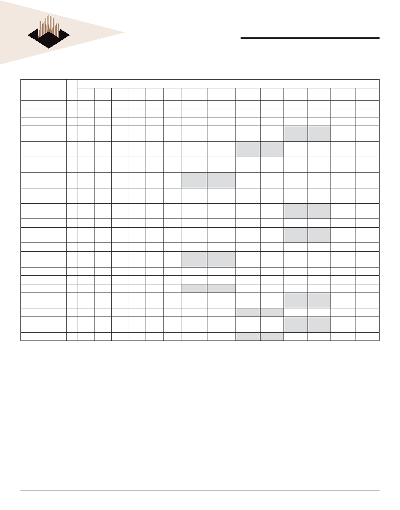
35
White Electronic Designs Corporation ∑ (602) 437-1520 ∑ www.wedc.com
White Electronic Designs
W78M64V-XSBX
December 2005
Rev. 3
White Electronic Designs Corp. reserves the right to change products or specifi cations without notice.
TABLE 14. SECTOR PROTECTION COMMAND DEFINITIONS
Command (Notes)
Cycles
Bus Cycles (Notes 1-4)
Addr
Data
Addr
Data
Addr
Data
Addr
Data
Addr
Data
Addr
Data
Addr
Data
Reset
1
XXX
F0
SecSi Sector Entry
3
555
AA
2AA
55
555
88
SecSi Sector Exit
4
555
AA
2AA
55
555
90
XX
00
SecSi Protection
Bit Program (5, 6)
6
555
AA
2AA
55
555
60
OW
68
OW
48
OW
RD (0)
Sector Protection
Bit Status
5
555
AA
2AA
55
555
60
OW
48
OW
RD(0)
Password
Program (5, 7, 8)
4
555
AA
2AA
55
555
38
XX[0-3]
PD[0-3]
Password Verify
(6, 8, 9)
4
555
AA
2AA
55
555
C8
PWA[0-3]
PWD[0-3]
Password Unlock
(7, 10, 11)
7
555
AA
2AA
55
555
28
PWA[0]
PWD[0]
PWA[1]
PWD[1]
PWA[2]
PWD[2]
PWA[3]
PWD[3]
PPB Program
(5, 6, 12)
6
555
AA
2AA
55
555
60
(SA)WP
68
(SA)WP
48
(SA)WP
RD(0)
PPB Status
4
555
AA
2AA
55
555
90
(SA)WP
RD(0)
All PPB Erase
(5, 6, 13, 14)
6
555
AA
2AA
55
555
60
WP
60
(SA)
40
(SA)WP
RD(0)
PPB Lock Bit Set
3
555
AA
2AA
55
555
78
PPB Lock Bit
Status (15)
4
555
AA
2AA
55
555
58
SA
RD(1)
DYB Write (7)
4
555
AA
2AA
55
555
48
SA
X1
DYB Erase (7)
4
555
AA
2AA
55
555
48
SA
X0
DYB Status (6)
4
555
AA
2AA
55
555
58
SA
48
PPMLB Program
(5, 6, 12)
6
555
AA
2AA
55
555
60
PL
68
PL
48
PL
RD(0)
PPMLB Status (5)
5
555
AA
2AA
55
555
60
PL
48
PL
RD(0)
SPMLB Program
(5, 6, 12)
6
555
AA
2AA
55
555
60
SL
68
SL
48
SL
RD(0)
SPMLB Status (5)
5
555
AA
2AA
55
555
60
SL
48
SL
RD(0)
Legend:
DYB = Dynamic Protection Bit
OW = Address (A7:A0) is (00011010)
PD[3:0] = Password Data (1 of 4 portions)
PPB = Persistent Protection Bit
PWA = Password Address. A1:A0 selects portion of password.
PWD = Password Data being verifi ed.
PL = Password Protection Mode Lock Address (A7:A0) is (00001010)
RD(0) = Read Data DQ0 for protection indicator bit.
RD(1) = Read Data DQ1 for PPB Lock status.
SA = Sector Address where security command applies. Address bits
A22:A12 uniquely select any sector.
SL = Persistent Protection Mode Lock Address (A7:A0) is (00010010)
WP = PPB Address (A7:A0) is (00000010)
X = Don't care
PPMLB = Password Protection Mode Locking Bit
SPMLB = Persistent Protection Mode Locking Bit
1. See
Table 1
for description of bus operations.
2. All values are in hexadecimal.
3. Shaded cells in table denote read cycles. All other cycles are write operations.
4. During unlock and command cycles, when lower address bits are 555 or 2AAh as
shown in table, address bits higher than A11 (except where BA is required) and data
bits higher than DQ7 are don't cares.
5. The reset command returns device to reading array.
6. Cycle 4 programs the addressed locking bit. Cycles 5 and 6 validate bit has been
fully programmed when DQ0 = 1. If DQ0 = 0 in cycle 6, program command must be
issued and verifi ed again.
7. Data is latched on the rising edge of WE#.
8. Entire command sequence must be entered for each portion of password.
9. Command sequence returns FFh if PPMLB is set.
10. The password is written over four consecutive cycles, at addresses 0-3.
11. A 2 µs timeout is required between any two portions of password.
12. A 100 µs timeout is required between cycles 4 and 5.
13. A 1.2 ms timeout is required between cycles 4 and 5.
14. Cycle 4 erases all PPBs. Cycles 5 and 6 validate bits have been fully erased when
DQ0 = 0. If DQ0 = 1 in cycle 6, erase command must be issued and verifi ed again.
Before issuing erase command, all PPBs should be programmed to prevent PPB
overerasure.
15. DQ1 = 1 if PPB locked, 0 if unlocked.

36
White Electronic Designs Corporation ∑ (602) 437-1520 ∑ www.wedc.com
White Electronic Designs
W78M64V-XSBX
December 2005
Rev. 3
White Electronic Designs Corp. reserves the right to change products or specifi cations without notice.
WRITE OPERATION STATUS
The device provides several bits to determine the status of
a program or erase operation: DQ2, DQ3, DQ5, DQ6, and
DQ7.
Table 15
and the following subsections describe the
function of these bits. DQ7 and DQ6 each offer a method
for determining whether a program or erase operation
is complete or in progress. The device also provides a
hardware-based output signal, RY/BY#, to determine
whether an Embedded Program or Erase operation is in
progress or has been completed.
DQ7: DATA# POLLING
The Data# Polling bit, DQ7, indicates to the host system
whether an Embedded Program or Erase algorithm is
in progress or completed, or whether a bank is in Erase
Suspend. Data# Polling is valid after the rising edge of the
fi nal WE# pulse in the command sequence.
During the Embedded Program algorithm, the device
outputs on DQ7 the complement of the datum programmed
to DQ7. This DQ7 status also applies to programming during
Erase Suspend. When the Embedded Program algorithm
is complete, the device outputs the datum programmed to
DQ7. The system must provide the program address to read
valid status information on DQ7. If a program address falls
within a protected sector, Data# Polling on DQ7 is active
for approximately 1 µs, then that bank returns to the read
mode.
During the Embedded Erase algorithm, Data# Polling
produces a "0" on DQ7. When the Embedded Erase
algorithm is complete, or if the bank enters the Erase
Suspend mode, Data# Polling produces a "1" on DQ7. The
system must provide an address within any of the sectors
selected for erasure to read valid status information on
DQ7.
After an erase command sequence is written, if all sectors
selected for erasing are protected, Data# Polling on DQ7
is active for approximately 400 µs, then the bank returns
to the read mode. If not all selected sectors are protected,
the Embedded Erase algorithm erases the unprotected
sectors, and ignores the selected sectors that are protected.
However, if the system reads DQ7 at an address within a
protected sector, the status may not be valid.
When the system detects DQ7 has changed from
the complement to true data, it can read valid data at
DQ15≠DQ0 on the following read cycles. Just prior to the
completion of an Embedded Program or Erase operation,
DQ7 may change asynchronously with DQ15≠DQ0 while
Output Enable (OE#) is asserted low. That is, the device
may change from providing status information to valid data
on DQ7. Depending on when the system samples the
DQ7 output, it may read the status or valid data. Even if
the device has completed the program or erase operation
and DQ7 has valid data, the data outputs on DQ15≠DQ0
may be still invalid. Valid data on DQ15≠DQ0 will appear
on successive read cycles.
Table 15
shows the outputs for Data# Polling on DQ7.
Figure 8 shows the Data# Polling algorithm. Figure 19
in the
AC Characteristic
section shows the Data# Polling
timing diagram.
DQ7 = Data?
Yes
No
No
DQ5 = 1?
No
Yes
Yes
PASS
Read DQ7≠DQ0
Addr = VA
Read DQ7≠DQ0
Addr = VA
DQ7 = Data?
START
FAIL
Notes:
1. VA = Valid address for programming. During a sector erase operation, a valid address
is any sector address within the sector being erased. During chip erase, a valid
address is any non-protected sector address.
2. DQ7 should be rechecked even if DQ5 = "1" because DQ7 may change
simultaneously with DQ5.
FIGURE 8. DATA# POLLING ALGORITHM

37
White Electronic Designs Corporation ∑ (602) 437-1520 ∑ www.wedc.com
White Electronic Designs
W78M64V-XSBX
December 2005
Rev. 3
White Electronic Designs Corp. reserves the right to change products or specifi cations without notice.
RY/BY#: READY/BUSY#
The RY/BY# is a dedicated, open-drain output pin which
indicates whether an Embedded Algorithm is in progress or
complete. The RY/BY# status is valid after the rising edge
of the fi nal WE# pulse in the command sequence. Since
RY/BY# is an open-drain output, several RY/BY# pins can
be tied together in parallel with a pull-up resistor to V
CC
.
If the output is low (Busy), the device is actively erasing
or programming. (This includes programming in the Erase
Suspend mode.) If the output is high (Ready), the device is
in the read mode, the standby mode, or one of the banks is
in the erase-suspend- read mode.
Table 15
shows the outputs for RY/BY#.
DQ6: TOGGLE BIT I
Toggle Bit I on DQ6 indicates whether an Embedded
Program or Erase algorithm is in progress or complete, or
whether the device has entered the Erase Suspend mode.
Toggle Bit I may be read at any address, and is valid after
the rising edge of the fi nal WE# pulse in the command
sequence (prior to the program or erase operation), and
during the sector erase time-out.
During an Embedded Program or Erase algorithm operation,
successive read cycles to any address cause DQ6 to
toggle. The system may use either OE# or CS# to control
the read cycles. When the operation is complete, DQ6
stops toggling.
After an erase command sequence is written, if all sectors
selected for erasing are protected, DQ6 toggles for
approximately 400 µs, then returns to reading array data. If
not all selected sectors are protected, the Embedded Erase
algorithm erases the unprotected sectors, and ignores the
selected sectors that are protected.
The system can use DQ6 and DQ2 together to determine
whether a sector is actively erasing or is erase-suspended.
When the device is actively erasing (that is, the Embedded
Erase algorithm is in progress), DQ6 toggles. When the
device enters the Erase Suspend mode, DQ6 stops toggling.
However, the system must also use DQ2 to determine which
sectors are erasing or erase-suspended. Alternatively, the
system can use DQ7 (see the subsection on
DQ7: Data#
Polling
).
If a program address falls within a protected sector, DQ6
toggles for approximately 1 µs after the program command
sequence is written, then returns to reading array data.
DQ6 also toggles during the erase-suspend-program mode,
and stops toggling once the Embedded Program algorithm
is complete.
Table 15
shows the outputs for Toggle Bit I on DQ6.
Figure 9 shows the toggle bit algorithm. Figure 20 in the
"AC Characteristics" section shows the toggle bit timing
diagrams. Figure 21 shows the differences between DQ2
and DQ6 in graphical form. See also the subsection on
DQ2: Toggle Bit II
.
START
No
Yes
Yes
DQ5 = 1?
No
Yes
Toggle Bit
= Toggle?
No
Program/Erase
Operation Not
Complete, Write
Reset Command
Program/Erase
Operation Complete
Toggle Bit
= Toggle?
Read Byte Twice
(DQ7≠DQ0)
Address = VA
Read Byte
(DQ7≠DQ0)
Address =VA
Read Byte
(DQ7≠DQ0)
Address =VA
Note: The system should recheck the toggle bit even if DQ5 = "1" because the toggle bit
may stop toggling as DQ5 changes to "1." See the subsections on DQ6 and DQ2
for more information.
FIGURE 9. TOGGLE BIT ALGORITHM

38
White Electronic Designs Corporation ∑ (602) 437-1520 ∑ www.wedc.com
White Electronic Designs
W78M64V-XSBX
December 2005
Rev. 3
White Electronic Designs Corp. reserves the right to change products or specifi cations without notice.
DQ2: TOGGLE BIT II
The "Toggle Bit II" on DQ2, when used with DQ6, indicates
whether a particular sector is actively erasing (that is, the
Embedded Erase algorithm is in progress), or whether
that sector is erase-suspended. Toggle Bit II is valid after
the rising edge of the fi nal WE# pulse in the command
sequence.
DQ2 toggles when the system reads at addresses within
those sectors that have been selected for erasure. (The
system may use either OE# or CS# to control the read
cycles.) But DQ2 cannot distinguish whether the sector is
actively erasing or is erase-suspended. DQ6, by comparison,
indicates whether the device is actively erasing, or is in
Erase Suspend, but cannot distinguish which sectors are
selected for erasure. Thus, both status bits are required for
sector and mode information. Refer to
Table 15
to compare
outputs for DQ2 and DQ6.
Figure 9 shows the toggle bit algorithm in fl owchart form, and
the section "DQ2: Toggle Bit II" explains the algorithm. See
also the
DQ6: Toggle Bit I
subsection. Figure 20 shows the
toggle bit timing diagram. Figure 21 shows the differences
between DQ2 and DQ6 in graphical form.
READING TOGGLE BITS DQ6/DQ2
Refer to Figure 9 for the following discussion. Whenever the
system initially begins reading toggle bit status, it must read
DQ7≠DQ0 at least twice in a row to determine whether a
toggle bit is toggling. Typically, the system would note and
store the value of the toggle bit after the fi rst read. After the
second read, the system would compare the new value of
the toggle bit with the fi rst. If the toggle bit is not toggling,
the device has completed the program or erase operation.
The system can read array data on DQ7≠DQ0 on the
following read cycle.
However, if after the initial two read cycles, the system
determines that the toggle bit is still toggling, the system
also should note whether the value of DQ5 is high (see
the section on DQ5). If it is, the system should then
determine again whether the toggle bit is toggling, since
the toggle bit may have stopped toggling just as DQ5 went
high. If the toggle bit is no longer toggling, the device has
successfully completed the program or erase operation. If
it is still toggling, the device did not completed the operation
successfully, and the system must write the reset command
to return to reading array data.
The remaining scenario is that the system initially determines
that the toggle bit is toggling and DQ5 has not gone high.
The system may continue to monitor the toggle bit and DQ5
through successive read cycles, determining the status as
described in the previous paragraph. Alternatively, it may
choose to perform other system tasks. In this case, the
system must start at the beginning of the algorithm when
it returns to determine the status of the operation (top of
Figure 9).
DQ5: EXCEEDED TIMING LIMITS
DQ5 indicates whether the program or erase time has
exceeded a specifi ed internal pulse count limit. Under these
conditions DQ5 produces a "1," indicating that the program
or erase cycle was not successfully completed.
The device may output a "1" on DQ5 if the system tries to
program a "1" to a location that was previously programmed
to "0." Only an erase operation can change a "0"
back to a "1." Under this condition, the device halts the
operation, and when the timing limit has been exceeded,
DQ5 produces a "1."
Under both these conditions, the system must write the
reset command to return to the read mode (or to the erase-
suspend-read mode if a bank was previously in the erase-
suspend-program mode).
DQ3: SECTOR ERASE TIMER
After writing a sector erase command sequence, the
system may read DQ3 to determine whether or not erasure
has begun. (The sector erase timer does not apply to the
chip erase command.) If additional sectors are selected
for erasure, the entire time-out also applies after each
additional sector erase command. When the time-out period
is complete, DQ3 switches from a "0" to a "1." See also the
Sector Erase Command Sequence
section.
After the sector erase command is written, the system should
read the status of DQ7 (Data# Polling) or DQ6 (Toggle Bit
I) to ensure that the device has accepted the command
sequence, and then read DQ3. If DQ3 is "1," the Embedded
Erase algorithm has begun; all further commands (except
Erase Suspend) are ignored until the erase operation is
complete. If DQ3 is "0," the device will accept additional
sector erase commands. To ensure the command has been
accepted, the system software should check the status of
DQ3 prior to and following each subsequent sector erase
command. If DQ3 is high on the second status check, the
last command might not have been accepted.
Table 15
shows the status of DQ3 relative to the other
status bits.

39
White Electronic Designs Corporation ∑ (602) 437-1520 ∑ www.wedc.com
White Electronic Designs
W78M64V-XSBX
December 2005
Rev. 3
White Electronic Designs Corp. reserves the right to change products or specifi cations without notice.
TABLE 15. WRITE OPERATION STATUS
Status
DQ7
(Note 2)
DQ6
DQ5
(Note 1)
DQ3
DQ2 (Note 2)
RY/BY#
Standard Mode
Embedded Program Algorithm
DQ7#
Toggle
0
N/A
No Toggle
0
Embedded Erase Algorithm
0
Toggle
0
1
Toggle
0
Erase Suspend
Mode
Erase-Suspend-
Read
Erase
Suspended Sector
1
Not toggle
0
N/A
Toggle
1
Non-Erase
Suspend Sector
Data
Data
Data
Data
Data
1
Erase-Suspend-Program
DQ7#
Toggle
0
N/A
N/A
0
Notes:
1. DQ5 switches to `1' when an Embedded Program or Embedded Erase operation has
exceeded the maximum timing limits. Refer to the section on DQ5 for more information.
2. DQ7 and DQ2 require a valid address when reading status information. Refer to the
appropriate subsection for further details.
3. When reading write operation status bits, the system must always provide the bank address
where the Embedded Algorithm is in progress. The device outputs array data if the system
addresses a non-busy bank

40
White Electronic Designs Corporation ∑ (602) 437-1520 ∑ www.wedc.com
White Electronic Designs
W78M64V-XSBX
December 2005
Rev. 3
White Electronic Designs Corp. reserves the right to change products or specifi cations without notice.
ABSOLUTE MAXIMUM RATINGS
(1, 2)
Parameter
Unit
Operating Temperature
-55 to +125
∞C
Supply Voltage Range (V
CC
)
-0.5 to +4.0
V
Storage Temperature Range
-55 to +125
∞C
Endurance (write/erase cycles)
1,000,000 min.
cycles
NOTES:
1. Stesses above the absolute maximum rating may cause permanent damage to the
device. Extended operation at the maximum levels may degrade performance and
affect reliability.
2.
Minimum DC input voltage on pins A9, OE#, RESET#, and WP#/ACC is ≠0.5V.
During voltage transitions, A9, OE#, WP#/ACC, and RESET# may overshoot V
SS
to
≠2.0V for periods of up to 20 ns. See
Figure 8
. Maximum DC input voltage on pin A9,
OE#, and RESET# is +12.5V which may overshoot to +14.0V for periods up to 20 ns.
Maximum DC input voltage on WP#/ACC is +9.5V which may overshoot to +12.0V
for periods up to 20 ns.
RECOMMENDED OPERATING CONDITIONS
Parameter
Symbol
Min
Max
Unit
Supply Voltage
V
CC
3.0
3.6
V
I/O Supply Voltage
V
IO
3.0
3.6
V
Operating Temp. (Mil.)
T
A
-55
+125
∞C
Operating Temp. (Ind.)
T
A
-40
+85
∞C
Note: For all AC and DC specifi cations: V
IO
= V
CC
CAPACITANCE
T
A
= +25∞C, f = 1.0MHz
Parameter
Symbol
Max
Unit
WE# capacitance
C
WE
12
pF
CS# capacitance
C
CS
13
pF
Data I/O capacitance
C
I/O
13
pF
Address input capacitance
C
AD
35
pF
RESET# capacitance
C
RS
35
pF
RY/BY#
C
RB
32
pF
OE# capacitance
C
OE
36
pF
This parameter is guaranteed by design but not tested.
DATA RETENTION
Parameter
Test Conditions
Min
Unit
Pattern Data
Retention Time
150∞C
10
Years
125∞C
20
Years
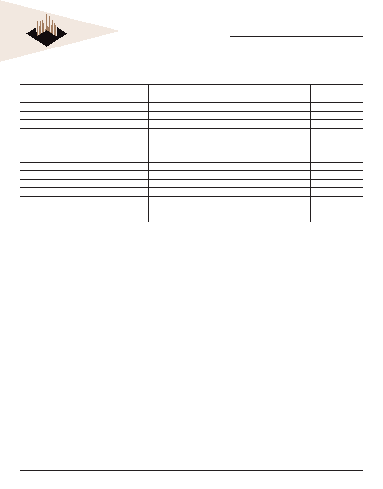
41
White Electronic Designs Corporation ∑ (602) 437-1520 ∑ www.wedc.com
White Electronic Designs
W78M64V-XSBX
December 2005
Rev. 3
White Electronic Designs Corp. reserves the right to change products or specifi cations without notice.
DC CHARACTERISTICS - CMOS COMPATABLE
V
CC
= 3.3V ± 0.3V. -55∞C T
A
+125∞C
Parameter Description
Symbol
Test Conditions
Min
Max
Unit
Input Load Current (Addresses)
I
LI
V
IN
=V
SS
to V
CC
, V
CC
=V
CC
max
-4
4
µA
Output Leakage Current
I
LO
V
OUT
= V
SS
to V
CC
, OE# = V
IH
, V
CC
= V
CC max
-1
1
µA
V
CC
Active Read Current (Notes 1, 2)
l
CC1
OE# = V
IH
, V
CC
= V
CC
max, f = 5 MHz (Note 1)
120
mA
V
CC
Active Write Current (Notes 2, 3)
I
CC2
OE# = V
IH
, WE# =V
IL
100
mA
V
CC
Standby Current (Note 2)
l
CC3
CS#, RESET#, WP/ACC# = V
IO
± 0.3 V
150
µA
Automatic Sleep Mode (Notes 2, 4, 5)
I
CC5
V
IH
= V
IO
± 0.3 V; V
IL
= V
SS
± 0.3 V
150
µA
V
CC
Active Read-While-Program Current (Notes 1, 2, 5)
I
CC6
OE# = V
IH
180
mA
V
CC
Active Read-While-Erase Current (Notes 1, 2, 5)
I
CC7
OE# = V
IH
180
mA
Input Low Voltage
V
IL
V
IO
= 3.3V ± 0.3V
-0.5
0.8
V
Input High Voltage
V
IH
V
IO
= 3.3V ± 0.3V
2.0
V
CC
+0.3
V
Voltage for ACC Program Acceleration
V
HH
V
CC
= 3.0 V ± 0.3V
8.5
9.5
V
Voltage for Autoselect and Temporary Sector Unprotect
V
ID
Vcc = 3.0 V ± 0.3V
11.5
12.5
V
Output Low Voltage
V
OL
I
OL
= 2.0 mA, V
CC
= V
CC
min
, V
IO
= 3.3V ± 0.3V
0.4
V
Output High Voltage
V
OH
I
OH
= -2.0 mA, V
CC
= V
CC
, V
IO
= 3.3V ± 0.3V
2.4
V
Low V
CC
Lock-Out Voltage (Note 5)
V
LKO
2.3
2.5
V
Notes:
1. The
l
CC
current listed is typically less than 5 mA/MHz, with OE# at V
IH
.
2. Maximum
l
CC
specifi cations are tested with V
CC
= V
CCMAX.
3. I
CC
active while Embedded Erase or Embedded Program is in progress.
4.
Automatic sleep mode enables the low power mode when addresses remain stable
for t
ACC
+ 150 ns. Typical sleep mode current is 4 µA.
5. Not
tested.

42
White Electronic Designs Corporation ∑ (602) 437-1520 ∑ www.wedc.com
White Electronic Designs
W78M64V-XSBX
December 2005
Rev. 3
White Electronic Designs Corp. reserves the right to change products or specifi cations without notice.
Current Source
Current Source
I
OL
I
OH
D.U.T.
C
= 50 pf
EFF
V ~ 1.5v
(Bipolar Supply)
Z
AC TEST CIRCUIT
FIG 10:
AC TEST CONDITIONS
Parameter
Typ
Unit
Input Pulse Levels
V
IL
- 0, V
IH
= 2.5
V
Input Rise and Fall
5
ns
Input and Output Reference Level
1.5
V
Output Timing Reference Level
1.5
V
Notes:
VZ is programmable from -2V to +7V.
IOL & IOH programmable from 0 to 16 mA.
Tester Impedance Z0 = 75
.
VZ is typically the midpoint of V
OH
and V
OL.
IOL & IOH are adjusted to similate a typical resistive load circuit.
ATE tester Includes jig capacitance.
AC CHARACTERISTICS - READ-ONLY OPERATIONS
V
CC
= 3.3V ± 0.3V, -55∞C T
A
+125∞C
Parameter
Symbol
-70Min
Max
-90
Min Max
-100
Min Max
-120
Min Max
Unit
Read Cycle Time (1)
t
AVAV
t
RC
70
90
100
120
ns
Address Access Time
t
AVAQV
t
ACC
70
90
100
120
ns
Chip Select Access Time
t
ELQV
t
CE
70
90
100
120
ns
Page Access Time (1)
t
PACC
70
90
100
120
ns
Output Enable to Output Valid
t
GLQV
t
OE
30
40
40
50
ns
Chip Select High to Output High Z
t
EHQZ
t
DF
20
20
20
20
ns
Output Enable High to Output High Z
t
GHQZ
t
DF
20
20
20
20
ns
Output Hold from Addresses, CS# or OE# Change,
Whichever occurs fi rst
t
AXQX
t
OH
5
5
5
ns
Output Enable Hold Time (1)
Read
t
OEH
0
0
0
Toggle and
Data# Polling
10
10
10
NOTE:
1.
Not tested.
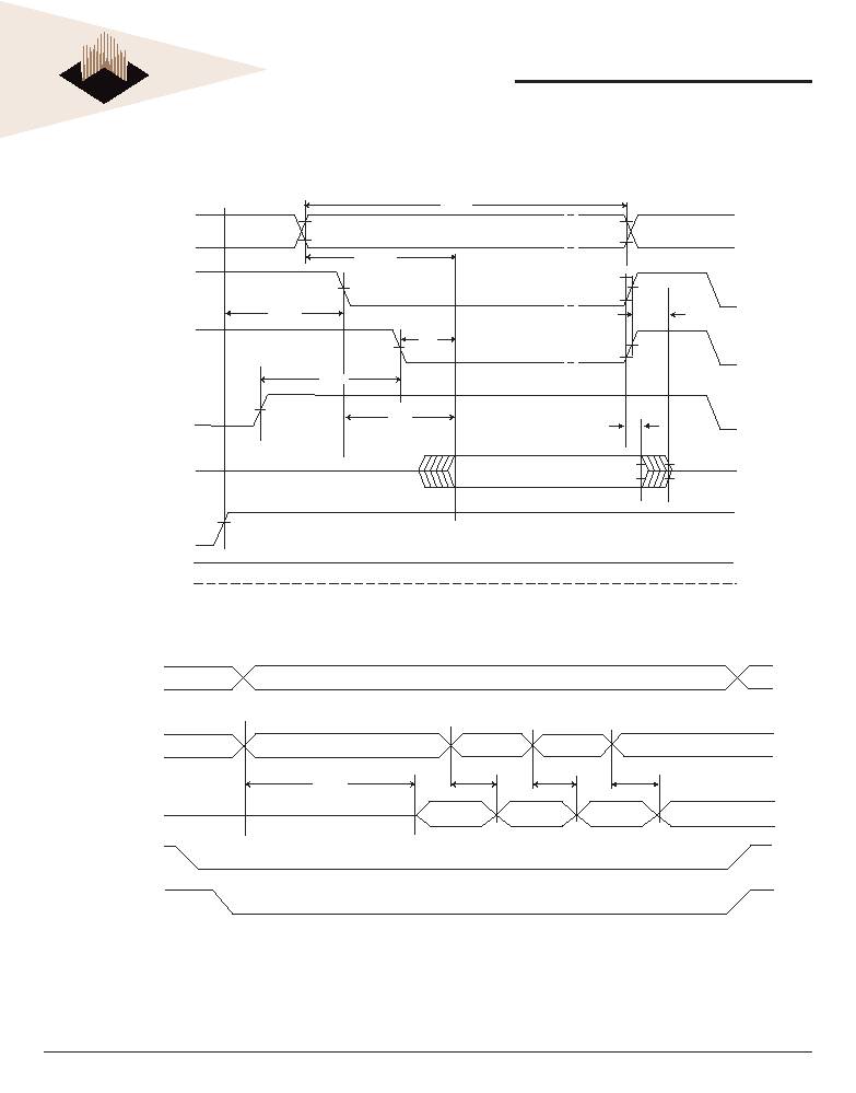
43
White Electronic Designs Corporation ∑ (602) 437-1520 ∑ www.wedc.com
White Electronic Designs
W78M64V-XSBX
December 2005
Rev. 3
White Electronic Designs Corp. reserves the right to change products or specifi cations without notice.
Addresses
Addresses Stable
t
RC
t
ACC
t
OE
t
OEH
t
CE
t
DF
t
OH
High Z
High Z
t
RH
CS#
OE#
WE#
Outputs
RESET#
RY/BY#
Output Valid
OV
A22-A3
A2-A0
Data
CS#
OE#
Aa
Ab
Ac
Ad
Qa
Qb
Qc
Qd
Same Page
t
ACC
t
PACC
t
PACC
t
PACC
FIG 11: AC WAVEFORMS FOR READ OPERATIONS
FIG 12: PAGE READ OPERATION TIMINGS
44
White Electronic Designs Corporation ∑ (602) 437-1520 ∑ www.wedc.com
White Electronic Designs
W78M64V-XSBX
December 2005
Rev. 3
White Electronic Designs Corp. reserves the right to change products or specifi cations without notice.
AC CHARACTERISTICS - HARDWARE RESET (1)
Parameter
Symbol
Min Max
Unit
RESET# Pin Low (During Embedded Algorithms)
to Read Mode
t
ready
20
µs
RESET# Pin Low (NOT During Embedded Algorithms)
to Read Mode
t
ready
500
ns
RESET# Pulse Width
t
RP
500
ns
RESET# High Time Before Read
t
RH
50
ns
RESET# Low to Standby Mode
t
RPD
20
µs
RY/BY# Recovery Time
t
RB
0
ns
NOTE:
1. Not tested.
RESET#
RY/BY#
RY/BY#
t
RP
t
Ready
t
Ready
CS#, OE#
t
RH
CS#, OE#
RESET#
t
RP
t
RB
FIG. 13: RESET TIMINGS NOT DURING EMBEDDED ALGORITHMS
FIG. 14: RESET TIMINGS DURING EMBEDDED ALGORITHMS

45
White Electronic Designs Corporation ∑ (602) 437-1520 ∑ www.wedc.com
White Electronic Designs
W78M64V-XSBX
December 2005
Rev. 3
White Electronic Designs Corp. reserves the right to change products or specifi cations without notice.
AC CHARACTERISTICS - WRITE/ERASE/PROGRAM OPERATIONS - WE# CONTROLLED
V
CC
= 3.3V ± 0.3V, -55∞C T
A
+125∞C
Parameter
Symbol
-70
Min Max
-90
Min Max
-100
Min Max
-120
Min Max
Unit
Write Cycle Time (3)
t
AVAV
t
WC
70
90
100
120
ns
Chip Select Setup Time (3)
t
ELWL
t
CS
0
0
0
0
ns
Write Enable Pulse Width
t
WLWH
t
WP
35
35
50
50
ns
Address Setup Time
t
AVWL
t
AS
0
0
0
0
ns
Data Setup Time
t
DVWH
t
DS
25
45
50
50
ns
Data Hold Time
t
WHDX
t
DH
0
0
0
0
ns
Address Hold Time
t
WLAX
t
AH
30
45
50
50
ns
Write Enable Pulse Width High (3)
t
WHWL
t
WPH
20
30
30
30
ns
Duration of Byte Programming
Operation (1)
t
WHWH1
300
300
300
300
µs
Sector Erase (2)
t
WHWH2
5
5
5
5
sec
Read Recovery Time before Write (3)
t
GHWL
0
0
0
0
ns
V
CC
Setup Time (3)
t
VCS
50
50
50
50
µs
Chip Programming Time (4)
200
200
200
200
sec
Address Setup Time to OE# low during
toggle bit polling
t
ASO
15
15
15
15
ns
Write Recovery Time from RY/BY# (3)
t
RB
0
0
0
0
ns
Program/Erase Valid to RY/BY#
t
BUSY
70
90
90
90
ns
Notes:
1. Typical value for t
WHWH1
is 6µs.
2. Typical value for t
WHWH2
is 0.5 sec.
3. Guaranteed by design, but not tested.
4. Typical value is 50 sec. The typical chip program time is considerably less than the maximum chip programming time listed, since most bytes program faster than the maximum program
times listed.

46
White Electronic Designs Corporation ∑ (602) 437-1520 ∑ www.wedc.com
White Electronic Designs
W78M64V-XSBX
December 2005
Rev. 3
White Electronic Designs Corp. reserves the right to change products or specifi cations without notice.
FIG. 15: PROGRAM OPERATION
OE#
WE#
CS#
V
Data
CC
Addresses
t
DS
t
AH
t
DH
t
WP
PD
t
WHWH1
t
WC
t
AS
t
WPH
t
VCS
555h
PA
PA
Read Status Data (last two cycles)
A0h
t
CS
Status
D
OUT
Program Command Sequence (last two cycles)
RY/BY#
t
RB
t
BUSY
t
CH
PA
NOTES:
1. PA is the address of the memory location to be programmed.
2. PD is the data to be programmed at byte address.
3. D
OUT
is the output of the data written to the device.

47
White Electronic Designs Corporation ∑ (602) 437-1520 ∑ www.wedc.com
White Electronic Designs
W78M64V-XSBX
December 2005
Rev. 3
White Electronic Designs Corp. reserves the right to change products or specifi cations without notice.
FIG 16: ACCELETATED PROGRAM TIMING DIAGRAM
WP#/ACC
t
VHH
V
HH
V or V
IL
IH
V
or V
IL
IH
t
VHH
FIG 17: CHIP/SECTOR ERASE OPERATION TIMINGS
OE#
WE#
CS#
V
Data
CC
Addresses
t
DS
t
AH
t
DH
t
WP
30h
t
WHWH2
t
WC
t
AS
t
WPH
t
VCS
2AAh
SA
VA
Read Status Data (last two cycles)
55h
t
CS
Status
D
OUT
Program Command Sequence (last two cycles)
RY/BY#
t
RB
t
BUSY
t
CH
VA
10 for Chip Erase
555h for
chip erase
Notes:
1.
SA = Sector Address (for Sector Erase), VA = Valid Address for reading status data (see "write operation status")

48
White Electronic Designs Corporation ∑ (602) 437-1520 ∑ www.wedc.com
White Electronic Designs
W78M64V-XSBX
December 2005
Rev. 3
White Electronic Designs Corp. reserves the right to change products or specifi cations without notice.
FIG 19: DATA# POLLING TIMINGS (DURING EMBEDDED ALGORITHMS)
FIG 18: BACK TO BACK READ/WRITE CYCLE TIMINGS
OE#
CS#
WE#
Addresses
t
OH
Data
Valid
In
Valid
In
Valid PA
Valid RA
t
WC
t
WPH
t
AH
t
WP
t
DS
t
DH
t
AS
t
RC
t
CS
t
AH
Valid
Out
t
OE
t
ACC
t
OEH
t
GHWL
t
DF
Valid
In
CS# Controlled Write Cycles
WE# Controlled Write Cycle
Valid PA
Valid PA
t
CP
t
CPH
t
WC
t
WC
Read Cycle
t
SR/W
t
AS
WE#
CS#
OE#
High Z
t
OE
High Z
DQ7
DQ6≠DQ0
RY/BY#
t
BUSY
Complement
True
Addresses
VA
t
OEH
t
CS
t
CH
t
OH
t
DF
VA
VA
Status Data
Complement
Status Data
True
Valid Data
Valid Data
t
ACC
t
RC
NOTE: VA = Valid address. Illustration shows fi rst status cycles after command sequence, last status read cycles, and array data read cycle.

49
White Electronic Designs Corporation ∑ (602) 437-1520 ∑ www.wedc.com
White Electronic Designs
W78M64V-XSBX
December 2005
Rev. 3
White Electronic Designs Corp. reserves the right to change products or specifi cations without notice.
FIG 21: DQ2 VS. DQ6
FIG 20: TOGGLE BIT TIMINGS (DURING EMBEDDED ALGORITHMS)
OE#
CS#
WE#
Addresses
t
OEH
t
DH
t
AHT
t
ASO
t
OEPH
t
OE
Valid Data
(first read)
(second read)
(stops toggling)
t
CSPH
t
AHT
t
AS
DQ6/DQ2
Valid Data
Valid
Status
Valid
Status
Valid
Status
RY/BY#
Enter
Erase
Erase
Erase
Enter Erase
Suspend Program
Erase Suspend
Read
Erase Suspend
Read
Erase
WE#
DQ6
DQ2
Erase
Complete
Erase
Suspend
Suspend
Program
Resume
Embedded
Erasing
NOTE: DQ2 toggles only when read at an address within an erase-suspended sector. The system may use OE# or CS# to toggle DQ2 and DQ6.

50
White Electronic Designs Corporation ∑ (602) 437-1520 ∑ www.wedc.com
White Electronic Designs
W78M64V-XSBX
December 2005
Rev. 3
White Electronic Designs Corp. reserves the right to change products or specifi cations without notice.
NOTES:
For sector protect, A6 = 0, A1 = 1, A0 = 0. For sector unprotect, A6 = 1, A1 = 1, A0 = 0.
FIG 22: SECTOR/SECTOR BLOCK PROTECT AND UNPROTECT TIMING DIAGRAM
Sector Group Protect: 150 µs
Sector Group Unprotect: 15 ms
1 µs
RESET#
SA, A6 ,
A1, A 0
Data
CS#
WE#
OE#
60h
60h
40h
Valid *
Valid *
Valid *
Status
Sector Group Protect/Unprotec t
Verify
V
ID
V
IH
AC CHARACTERISTICS - ALTERNATE CS# CONTROLLED ERASE AND PROGRAM OPERATIONS
Parameter
Description
Speed Options
Unit
JEDEC
Std
70
90
100
120
t
VAVAV
t
WS
Write Cycle Time (1)
Min
70
90
100
120
ns
t
AVWL
t
AS
Address Setup Time
Min
0
0
0
0
ns
t
ELAX
t
AH
Address Hold Time
Min
45
45
45
50
ns
t
DVEH
t
DS
Data Setup Time
Min
45
45
45
50
ns
t
EHDX
t
DH
Data Hold Time
Min
0
0
0
0
ns
t
GHEL
t
GHEL
Read Recovery Time Before Write (OE# High to WE# Low)
Min
0
0
0
0
ns
t
WLEL
t
WS
WE# Setup Time
Min
0
0
0
0
ns
t
EHWH
t
WH
WE# Hold Time
Min
0
0
0
0
ns
t
ELEH
t
CP
CS# Pulse Width
Min
35
35
45
50
ns
t
EHEL
t
CPH
CS# Pulse Width High (1)
Min
30
30
30
30
ns
t
WHWH1
t
WHWH1
Programming Operation
Typ
6
6
6
6
µs
t
WHWH1
t
WHWH1
Accelerated Programming Operation
Typ
4
4
4
4
µs
t
WHWH2
t
WHWH2
Sector Erase Operation
Typ
0.5
0.5
0.5
0.5
sec
NOTE:
1. Not tested.

51
White Electronic Designs Corporation ∑ (602) 437-1520 ∑ www.wedc.com
White Electronic Designs
W78M64V-XSBX
December 2005
Rev. 3
White Electronic Designs Corp. reserves the right to change products or specifi cations without notice.
FIG 23: ALTERNATE CS# CONTROLLED WRITE (ERASE/PROGRAM) OPERATION TIMINGS
t
GHEL
t
OE#
WS
CS#
WE#
RESET#
t
Data
DS
t
Addresses
AH
t
DH
t
CP
DQ7#
D
OUT
t
WC
t
AS
t
CPH
PA
Data# Polling
A0 for program
55 for erase
t
RH
t
WHWH1 or 2
RY/BY#
t
WH
PD for program
30 for sector erase
10 for chip erase
555 for program
2AA for erase
PA for program
SA for sector erase
555 for chip erase
t
BUSY
NOTES:
1.
Figure Indicated last two bus cycles of a program or erase operation.
2. PA = program address. SA = sector address, PD = program data.
3.
DQ7 is the complement of the data written to the device. D
OUT
is the data written to the device.

52
White Electronic Designs Corporation ∑ (602) 437-1520 ∑ www.wedc.com
White Electronic Designs
W78M64V-XSBX
December 2005
Rev. 3
White Electronic Designs Corp. reserves the right to change products or specifi cations without notice.
TEMPORARY SECTOR UNPROTECT
Parameter
Description
All Speed Options
Unit
JEDEC
Std
t
VIDR
V
ID
Rise and Fall Time (See Note)
Min
500
ns
t
VHH
V
HH
Rise and Fall Time (See Note)
Min
250
ns
t
RSP
RESET# Setup Time for Temporary Sector Unprotect
Min
4
µs
t
RRB
RESET# Hold Time from RY/BY# High for Temporary Sector
Unprotect
Min
4
µs
NOTE: Not tested.
RESET#
t
VIDR
V
ID
V
IL
or V
IH
V
ID
V
IL
or V
IH
CE#
WE#
RY/BY#
t
VIDR
t
RSP
Program or Erase Command Sequence
t
RRB
FIG 24: TEMPORARY SECTOR UNPROTECT TIMING DIAGRAM

53
White Electronic Designs Corporation ∑ (602) 437-1520 ∑ www.wedc.com
White Electronic Designs
W78M64V-XSBX
December 2005
Rev. 3
White Electronic Designs Corp. reserves the right to change products or specifi cations without notice.
PACKAGE: 159 PBGA (PLASTIC BALL GRID ARRAY)
9 8 7 6 5 4 3 2 1
10
A
B
C
D
E
F
G
H
J
K
L
M
N
P
R
T
22.15 (0.872) MAX
19.05
(0.750)
NOM
1.27
(0.050)
NOM
1.27 (0.050) NOM
11.43 (0.450) NOM
13.15 (0.518) MAX
0.61 (0.024) NOM
2.34 (0.092) MAX
159 X ÿ 0.762 (0.030) NOM
BOTTOM VIEW
ALL LINEAR DIMENSIONS ARE IN MILLIMETERS AND PARENTHETICALLY IN INCHES
ORDERING INFORMATION
W 7 8M64 V XXX SB X
White Eletronic Designs Corp.
Flash:
Organization, 8M x 64:
User
confi gurable as 2 x 8M x 32, or 4 x 8M x16
3.3V Power Supply:
Access Time (ns):
70
=
70ns
90
=
90ns
100
=
100ns
120
=
120ns
Package Type:
SB = 159 PBGA, 13mm x 22mm
Devise Grade:
M
=
Military
-55∞C
to
+125∞C
I
=
Industrial
-40∞C
to
+85∞C
C = Commercial
0∞C to +70∞C
.

54
White Electronic Designs Corporation ∑ (602) 437-1520 ∑ www.wedc.com
White Electronic Designs
W78M64V-XSBX
December 2005
Rev. 3
White Electronic Designs Corp. reserves the right to change products or specifi cations without notice.
Document Title
8Mx64 Flash 3.3V Page Mode Simultaneous Read/Write Operations Multi-Chip Package
Revision History
Rev #
History
Release Date
Status
Rev 0
Initial Release
June 2004
Advanced
Rev 1
Changes (Pg. 1, 54)
1.1 Change status to Preliminary
October 2004
Preliminary
Rev 2
Changes (Pg. 1, 41)
2.1 PCN# 05006
April 2005
Preliminary
Rev 3
Changes (All pages)
3.1 Change status to Final
3.2 Add 70 ns speed grade
3.3 Correct Manufacturer ID
3.4 Add capacitance data
3.5 Add V
IO
to Recommended Operating Conditions
3.6 Change ILI to -4 and 4 µA
3.7 Remove duplicate Read Operations Table
3.8 Add WE# Controlled Program Table
December 2005
Final