1
White Electronic Designs Corporation ∑ (602) 437-1520 ∑ www.wedc.com
White Electronic Designs
W7G1M32SVx-BN
W7G21M32SVx-BN
Feb. 2004
Rev. 2
PRELIMINARY*
DESCRIPTION
The W7G1M32SVx-BN and W7G21M32SVx-BN are
or ga nized as one and two banks of 1Mx32 re spec tive ly.
The modules are based on AMDs AM29LV160DT - 1Mx16
or STs M29W160ET (optional) Flash device in TSOP
packages which are mount ed on an FR4 sub strate.
Both modules offer access times between 70 and 120ns
allowing for operation of high-speed mi cro pro ces sors
without wait states.
FEATURES
1Mx32 and 2x1Mx32 Densities
Based on AMD ≠ AM29LV160DT Flash Device
STs M29W160ET (optional)
Fast Read Access Time ≠ 70ns
3.3V Only Reprogramming
Flexible,
Sector
Architecture
∑ One 16Kbyte, two 8Kbyte, one 32Kbyte and
thirty-one 64Kbyte sectors.
∑ Any combination of sectors can be erased
∑ Also supports full chip erase
Top boot block confi gurations
∑ Bottom boot block optional. Contact WEDC.
W7G1M32SVx-BN: 1Mx32 80 PIN SIMM
W7G21M32SVx-BN: 2x1Mx32 80 PIN SIMM
8MB/4MB (2x1Mx32 / 1Mx32) CMOS, Boot Sector Flash
Memory Module
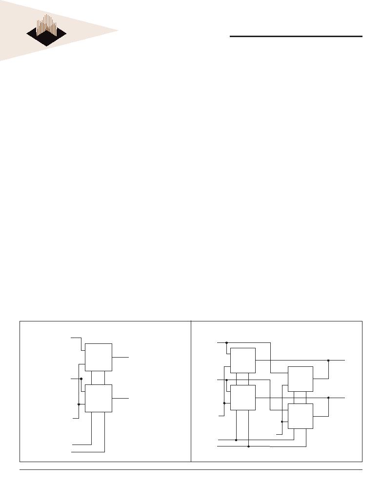
FIG. 1 ≠ BLOCK DIAGRAMS
DQ16-31
1Mx16
WE#
CE#
CE#
Addr
0-19
DQ0-15
WE2#
DQ0-15
1Mx16
WE#
CE#
CE0#
OE#
CE#
Addr
0-19
Addr 0-19
DQ0-15
WE0#
1Mx16
WE#
CE#
CE#
Addr
0-19
DQ0-15
WE2#
1Mx16
WE#
CE#
CE0#
OE#
CE#
Addr
0-19
Addr 0-19
DQ0-15
WE0#
DQ16-31
1Mx16
WE#
CE#
CE#
Addr
0-19
DQ0-15
DQ0-15
1Mx16
WE#
CE#
CE1#
CE#
Addr
0-19
DQ0-15
Embedded
Erase
Algorithms
∑ Automatically preprograms and erases the chip
or any combination of sectors
Embedded
Program
Algorithms
∑ Automatically programs and verifi es data at
specifi ed ad dress
Data Polling and Toggle Bit feature for detection of
pro gram or erase cycle completion
Low Power Dissipation
∑ 30mA per Device Active Current
∑ 10µA per Device CMOS Standby Current
Single 3.3V ±10% Supply
CMOS and TTL Compatible Inputs and Outputs
Commercial and industrial operating temperature
range
∑ BNC = 0∞C to 70∞C Commercial
∑ BNI = -40∞C to 85∞C Industrial
Package
∑ 80 Pin SIMM (JEDEC) Standard
* This product is under development, is not qualifi ed or characterized and is subject to
change without notice.

2
White Electronic Designs Corporation ∑ (602) 437-1520 ∑ www.wedc.com
White Electronic Designs
W7G1M32SVx-BN
W7G21M32SVx-BN
Feb. 2004
Rev. 2
PRELIMINARY
FIGURE 2 ≠ DECOUPLING CAPACITORS ARE PROVIDED FOR IMPROVED NOISE IMMUNITY.
Notes:
Unless otherwise specifi ed.
1. Population Confi guration for 1M x 32 Version
Part
Number
Confi
guration
Component
W7G1M32SVxxxBNX
1M x 32
1M x 8
2. Population Confi guration for 2 x 1M x 32 Version
Part
Number
Confi
guration
Component
W7G21M32SVxxxBNX
2 x 1M x 32
1M x 8
xx = Speed: 70, 90, 120ns
X = Temerature Range
Please refer to part number matrix pg. 8 or 9
V
CC
1
2
1
2
1
2
1
2
1
2
1
2
1
2
1
2
C1
.1 µF
C2
.1 µF
C3
.1 µF
C4
.1 µF
C5
.1 µF
C6
.1 µF
C7
.1 µF
C8
.1 µF
3
White Electronic Designs Corporation ∑ (602) 437-1520 ∑ www.wedc.com
White Electronic Designs
W7G1M32SVx-BN
W7G21M32SVx-BN
Feb. 2004
Rev. 2
PRELIMINARY
FIGURE 3 ≠ W7G1M32SVxxxBNX & W7G21M32SVxxxBNX PIN CONFIGURATION
Pin
Symbol
Pin
Symbol
Pin
Symbol
Pin
Symbol
1
GND
21
CE3
41
A11
61
DQ9
2
V
CC
22
CE2
42
A10
62
DQ8
3
NC
23
CE1
43
A9
63
DQ7
4
OE#
24
CE0
44
A8
64
DQ6
5
WE0#
25
GND
45
A7
65
DQ5
6
NC
26
DQ29
46
A6
66
DQ4
7
NC*
27
DQ30
47
A5
67
DQ3
8
DQ16
28
DQ31
48
A4
68
DQ2
9
DQ17
29
WE2#
49
A3
69
DQ1
10
DQ18
30
NC
50
A2
70
DQ0
11
DQ19
31
NC
51
A1
71
NC
12
DQ20
32
NC
52
A0
72
V
CC
13
DQ21
33
A19
53
NC
73
PD1
14
DQ22
34
A18
54
GND
74
PD2
15
DQ23
35
A17
55
DQ15
75
PD3
16
DQ24
36
A16
56
DQ14
76
PD4
17
DQ25
37
A15
57
DQ13
77
PD5
18
DQ26
38
A14
58
DQ12
78
PD6
19
DQ27
39
A13
59
DQ11
79
PD7
20
DQ28
40
A12
60
DQ10
80
GND
Notes:
Unless otherwise specifi ed.
1. Population Confi guration for 1M x 32 Version
Part
Number
Confi
guration
Component
W7G1M32SVxxxBNX
1M x 32
1M x 8
2. Population Confi guration for 2 x 1M x 32 Version
Part
Number
Confi
guration
Component
W7G21M32SVxxxBNX
2 x 1M x 32
1M x 8
xx = Speed: 70, 90, 120ns
X = Temerature Range
Please refer to part number matrix pg. 8 or 9
NC* = Pin 7 can offer custom module options. For optional "Reset" or
"Ready Busy." Contact WEDC.
PIN NAMES
A0 - A19
Address
DQ0 - DQ31
Data Input/Output
CE1#, CE2#
Chip Enable
WE0#, WE2#
Write Enable
OE#
Output Enable
V
CC
Power Supply
NC
No Connection
PD
Presence Detect
GND
Ground
4
White Electronic Designs Corporation ∑ (602) 437-1520 ∑ www.wedc.com
White Electronic Designs
W7G1M32SVx-BN
W7G21M32SVx-BN
Feb. 2004
Rev. 2
PRELIMINARY
PRESENCE DETECT TRUTH TABLE
Module Organization
PD1
PD2
PD3
PD4
1M x 32
1
0
1
0
2 x 1M x 32
0
1
0
0
MODULE SPEED IDENTIFICATION PRESENCE DETECT PIN
Speed
PD5
PD6
PD7
70 ns
0
0
1
90 ns
1
1
0
120 ns
0
1
0
LEGEND: 0 = Connected to GND
1 = Open circuit (no connection)
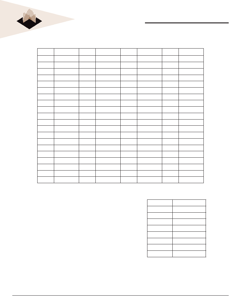
CAPACITANCE
f = 1.0MH
Z
, V
IN
= V
CC
or V
SS
Parameter
Symbol
1Meg
2x1Meg
Unit
Max
Max
Address Lines
CA
35
70
pF
Data lines
CDQ
15
30
pF
Chip & Write Enable Lines
CC
15
30
pF
Output Enable lines
CG
35
70
pF

5
White Electronic Designs Corporation ∑ (602) 437-1520 ∑ www.wedc.com
White Electronic Designs
W7G1M32SVx-BN
W7G21M32SVx-BN
Feb. 2004
Rev. 2
PRELIMINARY
Storage Temperature
Plastic Packages ................................. ≠65∞C to +150∞C
Ambient Temperature
with Power Applied ............................... ≠65∞C to +125∞C
Voltage with Respect to Ground
V
CC
(Note 1) ...................................... ≠0.5 V to +4.0 V
A9, OE#, and RESET# (Note 2) ...... ≠0.5 V to +12.5 V
All other pins (Note 1) .................. ≠0.5 V to V
CC
+0.5 V
Output Short Circuit Current (Note 3) ................. 200 mA
ABSOLUTE MAXIMUM RATINGS
Notes:
1.
Minimum DC voltage on input or I/O pins is ≠0.5 V. During voltage transitions,
input or I/O pins may overshoot VSS to ≠2.0 V for periods of up to 20 ns. See
Figure 7. Maximum DC voltage on input or I/O pins is VCC +0.5 V. During voltage
transitions, input or I/O pins may overshoot to VCC +2.0 V for periods up to 20
ns. See Figure 8.
2.
Minimum DC input voltage on pins A9, OE#, and RESET# is -0.5 V. During
voltage transitions, A9, OE#, and RESET# may overshoot VSS to ≠2.0 V for
periods of up to 20 ns. See Figure 7. Maximum DC input voltage on pin A9 is
+12.5 V which may overshoot to 14.0 V for periods up to 20 ns.
3.
No more than one output may be shorted to ground at a time. Duration of the
short circuit should not be greater than one second.
Stresses above those listed under "Absolute Maximum Ratings" may cause permanent
damage to the device. This is a stress rating only; functional operation of the device at
these or any other conditions above those indicated in the operational sections of this
data sheet is not implied. Exposure of the device to absolute maximum rating conditions
for extended periods may affect device reliability.
OPERATING RANGES
Commercial (C) Devices
Ambient Temperature (TA) ........................ 0∞C to +70∞C
Industrial (I) Devices
Ambient Temperature (TA) .................... ≠40∞C to +85∞C
V
CC
Supply Voltages
V
CC
for all devices .................................... 2.7 V to 3.6 V
Operating ranges defi ne those limits between which the functionality of the device is
guaranteed.
6
White Electronic Designs Corporation ∑ (602) 437-1520 ∑ www.wedc.com
White Electronic Designs
W7G1M32SVx-BN
W7G21M32SVx-BN
Feb. 2004
Rev. 2
PRELIMINARY
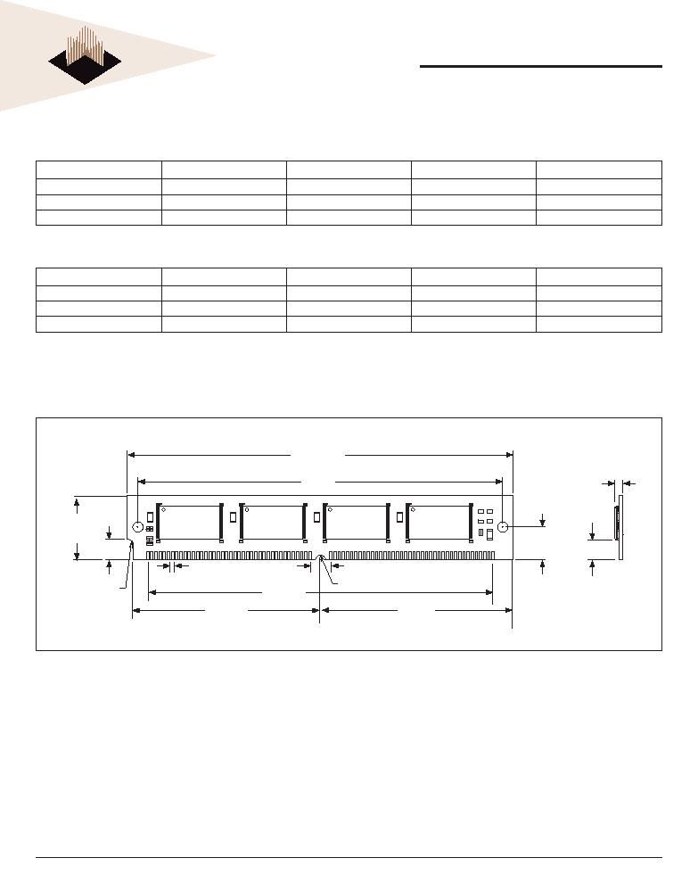
ORDERING IN FOR MA TION FOR W7G1M32SVx
PACKAGE NO. 346: 80 PIN SIMM (JEDEC)
J1
J3
153
1.57
(0.062) R
1.57 (0.062) R
21.59
(0.850)
MAX
118.24
(4.655) MAX.
111.35
(4.384)
6.35
(0.250)
57.02
(2.245)
55.68
(2.192)
10.16
(0.400)
105.41
(4.150)
1.27
(0.050) TYP
6.35 (0.250)
3.05
(0.120)
MAX
3.18
(0.125)
MIN
R3
R1
COMMERCIAL
Part Num ber
Speed (ns)
Pack age
T
A
Commercial Range
Height*
W7G1M32SVx70BNC
70
346
0∞C to +70∞C
21.59 (0.850")
W7G1M32SVx90BNC
90
346
0∞C to +70∞C
21.59 (0.850")
W7G1M32SVx120BNC
120
346
0∞C to +70∞C
21.59 (0.850")
INDUSTRIAL
Part Num ber
Speed (ns)
Pack age
T
A
Industrial Range
Height*
W7G1M32SVx70BNI
70
346
-40∞C to +85∞C
21.59 (0.850")
W7G1M32SVx90BNI
90
346
-40∞C to +85∞C
21.59 (0.850")
W7G1M32SVx120BNI
120
346
-40∞C to +85∞C
21.59 (0.850")
* ALL DIMENSIONS ARE IN MILLIMETERS AND (INCHES)

7
White Electronic Designs Corporation ∑ (602) 437-1520 ∑ www.wedc.com
White Electronic Designs
W7G1M32SVx-BN
W7G21M32SVx-BN
Feb. 2004
Rev. 2
PRELIMINARY
ORDERING IN FOR MA TION FOR W7G21M32SVx
PACKAGE NO. 361: 80 PIN SIMM (JEDEC)
5.72
(0.225)
MIN
3.18
(0.125)
MIN
4.32
(0.170)
MAX
J1
J3
153
1.57
(0.062) R
1.57 (0.062) R
21.59
(0.850)
MAX
118.24
(4.655) MAX.
111.35
(4.384)
6.35
(0.250)
57.02
(2.245)
55.68
(2.192)
10.16
(0.400)
105.41
(4.150)
1.27
(0.050) TYP
6.35 (0.250)
R3
R1
COMMERCIAL
Part Num ber
Speed (ns)
Pack age
T
A
Commercial Range
Height*
W7G21M32SVx70BNC
70
361
0∞C to +70∞C
21.59 (0.850")
W7G21M32SVx90BNC
90
361
0∞C to +70∞C
21.59 (0.850")
W7G21M32SVx120BNC
120
361
0∞C to +70∞C
21.59 (0.850")
INDUSTRIAL
Part Num ber
Speed (ns)
Pack age
T
A
Industrial Range
Height*
W7G21M32SVx70BNI
70
361
-40∞C to +85∞C
21.59 (0.850")
W7G21M32SVx90BNI
90
361
-40∞C to +85∞C
21.59 (0.850")
W7G21M32SVx120BNI
120
361
-40∞C to +85∞C
21.59 (0.850")
* ALL DIMENSIONS ARE IN MILLIMETERS AND (INCHES)

8
White Electronic Designs Corporation ∑ (602) 437-1520 ∑ www.wedc.com
White Electronic Designs
W7G1M32SVx-BN
W7G21M32SVx-BN
Feb. 2004
Rev. 2
PRELIMINARY
FLASH PART NUMBER MATRIX
W 7 G 1 M 3 2 S V X X X B N X
White Electronics Design
Flash
FR4 with gold contacts
Module Address depth: 1M
Module Bus width: x32
Component width: x16
Voltage: 3.3V
T = Top / B = Bottom Boot Block
Speed: 70, 90, 120
Package: 80 Pin SIMM
Temperature range:
C = 0∞C to 70∞C Commercial
I = -40∞C to 85∞C Industrial
9
White Electronic Designs Corporation ∑ (602) 437-1520 ∑ www.wedc.com
White Electronic Designs
W7G1M32SVx-BN
W7G21M32SVx-BN
Feb. 2004
Rev. 2
PRELIMINARY
W 7 G 2 1 M 3 2 S V X X X B N X
FLASH PART NUMBER MATRIX
White Electronics Design
Flash
FR4 with gold contacts
Bank
Module Address depth: 1M
Module Bus width: x32
Component width: x16
Voltage: 3.3V
T = Top / B = Bottom Boot Block
Speed: 70, 90, 120
Package: 80 Pin SIMM
Temperature range:
C = 0∞C to 70∞C Commercial
I = -40∞C to 85∞C Industrial

10
White Electronic Designs Corporation ∑ (602) 437-1520 ∑ www.wedc.com
White Electronic Designs
W7G1M32SVx-BN
W7G21M32SVx-BN
Feb. 2004
Rev. 2
PRELIMINARY
Document Title
8MB/4MB (2x1Mx32 / 1Mx32) CMOS, Boot Sector Flash Memory
Revision History
Rev #
History
Release Date
Status
Rev 0
Created
2-04
Advanced
Rev 1
Added T/B (top or bottom boot block option)
4-04
Advanced
Rev 2
Changed status from advanced to preliminary
6-04
Preliminary