
March 2006
Rev. 2
W7NCFxxx-H Series
1
White Electronic Designs Corporation ∑ (602) 437-1520 ∑ www.wedc.com
White Electronic Designs
PRELIMINARY*
FEATURES
Storage
Capacities:
∑
128MB, 256MB, 512MB, 2GB, and 4GB
Suitable for industrial temp (-40 to +85∞C) and
extended environment applications
CompactFlash
TM
Compatibility
∑
CFA standard 2.1 compliant
∑
3.3V or 5.0V single power supply
∑
50 pin connector with Type-I form factor (3.3mm
thickness)
∑
256 bytes of attribute memory
RoHS
compliant
Interface
modes
∑ PC
card
memory
model
∑
PC card I/O mode
∑ True
IDE
mode
Less than 1 Error in 10
14
bits read
MTBF > 4,000,000 hours
High shock & vibration tolerance
W/E
Endurance:
4,000,000
write/erase
cycles
High
performance
∑
Interface Transfer speed in PIO mode 4 or Multi
Word DMA mode 2 cycle timing; up to 16.7
MB/second (PIO mode 3 & 4 are available in
IDE mode only).
∑
Typical write: 5.0 MBytes/s in ATA PIO mode 4
∑
Typical write: 7.0 MBytes/s in ATA PIO mode 4
∑
On card ECC up to 6 Bytes per 512 Byte data
sector
Dimensions:
∑
Type I card : 36.4mm(L) x 42.8mm(W) x
3.3mm(H)
CompactFlash
TM
Card
Compact Flash
Æ
1
GB
Compact Flash
Æ
2
GB
Compact Flash
Æ
256
MB
DESCRIPTION
The W7NCFxxx-H Series CompactFlash
TM
card is an ATA
interface fl ash memory card based on fl ash technology.
The CompactFlash
TM
card is constructed with a 32 bit RISC
based controller and NAND fl ash memory devices. The
card operates from a single 5-Volt or 3.3-Volt power source,
and is available in CompactFlash
TM
type-I form factor with
128MB, 256MB, 512, 1GB, 2GB, and 4GB capacity. Able
to emulate IDE hard disk drives and certifi ed in accordance
with the CompactFlash
TM
Certifi cation Plan.
*This product is not fully characterized and is subject to change without notice.
CompactFlash
TM
is a trademark of SanDisk Corporation and is licensed royalty-free to
the CFA, which in turn will license it royalty-free to CFA members.
CFA: CompactFlash
TM
Association.
PRODUCT DENSITY
Card Density
Part Number
128MByte
W7NCF128H10IS2BG
256MByte
W7NCF256H10IS3BG
512MByte
W7NCF512H10IS4BG
1GByte
W7NCF01GH10IS4BG
2GByte
W7NCF02GH10IS6BG
4GByte
W7NCF04GH10IS7BG
March 2006
Rev. 2
W7NCFxxx-H Series
2
White Electronic Designs Corporation ∑ (602) 437-1520 ∑ www.wedc.com
White Electronic Designs
PRELIMINARY*
ENVIRONMENTAL CHARACTERIZATION
Item
Performance
Temperature
JEDEC - JESD STD A104 Temp condition N (-40∞C to 85 ∞C) and soak mode 3; 200 cycles
Humidity
MIL-STD 810F, Method 507.4, Paragraph 4.5.2 - 10 day test per fi gure 507.4-1, 10 day test
Vibration
MIL-STD 810F, Method 514.5, procedure 1, category 24, 1 hour per axis
Shock
MIL-STD 810F, Method 516.5, procedure1, non-operational, 40g, SRS functional shock for ground equipment, three (3)
shock per axis (positive or negative).
JEDEC- JESD22-B, 104-A, test condition B,1500 g pulse, 0.5 msec
Altitude
MIL-STD 810F, Method 500.4, procedure II, modifi ed to 80,000 ft and non operation 1 hr test duration at altitude
PRODUCT PERFORMANCE
Item
Performance (PIO mode 4 true IDE)
Read Transfer Rate (Typical)
7MB/s
Write Transfer Rate (Typical)
5MB/s
Burst Transfer Rate
up to 16.7MB/s
Controller Overhead
(Command to DRQ)
1ms typical, 5ms (max)
DC ELECTRICAL CHARACTERISTICS
Parameter
When DC input voltage is 3.3V +/- .3
Read Current (Typical)
Write Current (Typical)
Sleep (Typical standby Current)
W7NCF128H10IS2BG
60mA
60mA
200µA
W7NCF256H10IS3BG
60mA
60mA
200µA
W7NCF512H10IS4BG
70mA
70mA
200µA
W7NCF01GH10IS4BG
80mA
80mA
220µA
W7NCF02GH10IS6BG
80mA
80mA
220µA
W7NCF04GH10IS7BG
140mA
140mA
280µA
When DC input voltage is 5.0V +/- .5
W7NCF128H10IS2BG
60mA
60mA
200µA
W7NCF256H10IS3BG
60mA
60mA
200µA
W7NCF512H10IS4BG
70mA
70mA
200µA
W7NCF01GH10IS4BG
80mA
80mA
220µA
W7NCF02GH10IS6BG
80mA
80mA
220µA
W7NCF04GH10IS7BG
140mA
140mA
280µA
PRODUCT RELIABILITY
Item
Value
MTBF (@ 25∞C)
> 4,000,000 Hours
Data reliability
> 1 Non-Recoverable Error in 10
14
Bits Read
Endurance
> 4,000,000 write/erase cycles
March 2006
Rev. 2
W7NCFxxx-H Series
3
White Electronic Designs Corporation ∑ (602) 437-1520 ∑ www.wedc.com
White Electronic Designs
PRELIMINARY*
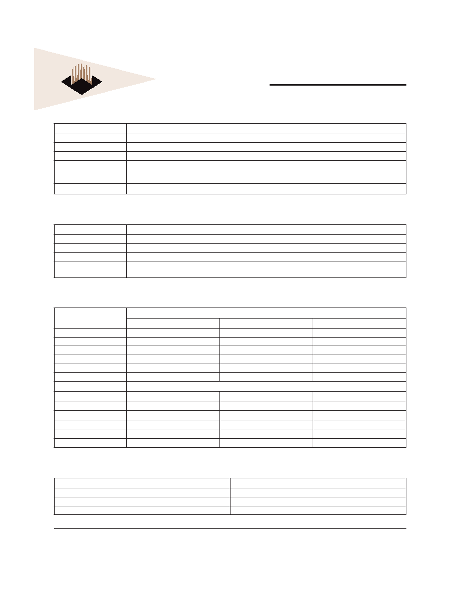
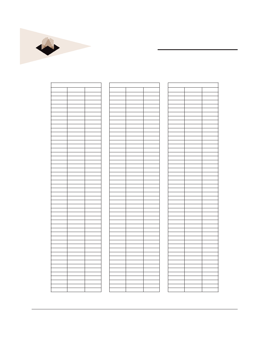
Pin Assignments & Pin Type
PC Card Memory Mode
Pin Number Signal Name
Pin Type
1
GND
2
D03
I/O
3
D04
I/O
4
D05
I/O
5
D06
I/O
6
D07
I/O
7
-CE1
I
8
A10
I
9
-OE
I
10
A09
I
11
A08
I
12
A07
I
13
V
CC
14
A06
I
15
A05
I
16
A04
I
17
A03
I
18
A02
I
19
A01
I
20
A00
I
21
D00
I/O
22
D01
I/O
23
D02
I/O
24
WP
O
25
-CD2
O
26
-CD1
O
27
D11
1
I/O
28
D12
1
I/O
29
D13
1
I/O
30
D14
1
I/O
31
D15
1
I/O
32
-CE21
I
33
-VS1
O
34
-IORD
I
35
-IOWR
I
36
-WE
I
37
RDY
O
38
V
CC
39
-CSEL
I
40
-VS2
O
41
RESET
I
42
-WAIT
O
43
-INPACK
O
44
-REG
I
45
BVD
2
I/O
46
BVD
1
I/O
47
DO8
1
I/O
48
DO9
1
I/O
49
D10
1
I/O
50
GND
PC Card I/O Mode
Pin Number Signal Name
Pin Type
1
GND
2
D03
I/O
3
D04
I/O
4
D05
I/O
5
D06
I/O
6
D07
I/O
7
-CE1
I
8
A10
I
9
-OE
I
10
A09
I
11
A08
I
12
A07
I
13
V
CC
14
A06
I
15
A05
I
16
A04
I
17
A03
I
18
A02
I
19
A01
I
20
A00
I
21
D00
I/O
22
D01
I/O
23
D02
I/O
24
-IOIS16
O
25
-CD2
O
26
-CD1
O
27
D11
1
I/O
28
D12
1
I/O
29
D13
1
I/O
30
D14
1
I/O
31
D15
1
I/O
32
-CE21
I
33
-VS1
O
34
-IORD
I
35
-IOWR
I
36
-WE
I
37
IREQ
O
38
V
CC
39
-CSEL
I
40
-VS2
O
41
RESET
I
42
-WAIT
O
43
-INPACK
O
44
-REG
I
45
BVD
2
I/O
46
BVD
1
I/O
47
DO8
1
I/O
48
DO9
1
I/O
49
D10
1
I/O
50
GND
True IDE Mode
Pin Number Signal Name
Pin Type
1
GND
2
D03
I/O
3
D04
I/O
4
D05
I/O
5
D06
I/O
6
D07
I/O
7
-CS0
I
8
A10
2
I
9
-ATA SEL
I
10
A09
2
I
11
A08
2
I
12
A07
2
I
13
V
CC
14
A06
2
I
15
A05
2
I
16
A04
2
I
17
A03
2
I
18
A02
I
19
A01
I
20
A00
I
21
D00
I/O
22
D01
I/O
23
D02
I/O
24
-IOIS16
O
25
-CD2
O
26
-CD1
O
27
D11
1
I/O
28
D12
1
I/O
29
D13
1
I/O
30
D14
1
I/O
31
D15
1
I/O
32
-CE21
I
33
-VS1
O
34
-IORD
I
35
-IOWR
I
36
-WE
3
I
37
IREQ
O
38
V
CC
39
-CSEL
I
40
-VS2
O
41
RESET
I
42
-WAIT
O
43
-INPACK
O
44
-REG
I
45
BVD
2
I/O
46
BVD
1
I/O
47
DO8
1
I/O
48
DO9
1
I/O
49
D10
1
I/O
50
GND
Note:
1
: These signals are required only for 16-bit access and are not required when
installed in 8-bit systems. Devices should allow for 3-state signals not to
consume current.
2
: Should be grounded by the host system.
3
: Should be tied to V
CC
by the host system.
-
Indicates enabled low

March 2006
Rev. 2
W7NCFxxx-H Series
4
White Electronic Designs Corporation ∑ (602) 437-1520 ∑ www.wedc.com
White Electronic Designs
PRELIMINARY*
ALL DIMENSIONS ARE IN MILLIMETERS AND (INCHES)
4xR 0.5mm ± .1
(4xR.020 in ± .004)
41.66mm ± .13(1.640 in ±. 005)
42.80mm ± .10(1.685 in ± .004)
0.63mm ± .07(.025 in ± .003)
.01mm ± .07(.039 in ± .003)
26
50
1
25
.99mm ± .05
(.039 in ± .002)
.01mm ± .07(.039 in ± .003)
3.30mm ± .10
(.130 in ± .004)
1.60mm ± .05
(.063 in ± .002)
0.76mm ± .07(0.30 in ± .003)
m
m
0
0
.
3
x
2±
7
0
.
n
i
8
1
1
.
x
2
(
.
±
)
3
0
0
m
m
0
4
.
6
3
±
n
i
3
3
4
.
1
(
5
1
.±
.
)
6
0
0
m
m
8
7
.
5
2
x
2±
5
1
0
.
1
x
2
(
7
0
.±
.
)
3
0
0
m
m
0
0
.
2
1
x
2±
0
1
.
n
i
2
7
4
x
2
(.
±)
4
0
0
2.15mm ± .07
(.085 in x .003)
Top View
PACKAGE DIMENSIONS

March 2006
Rev. 2
W7NCFxxx-H Series
5
White Electronic Designs Corporation ∑ (602) 437-1520 ∑ www.wedc.com
White Electronic Designs
PRELIMINARY*
Part Numbering Guide
W 7N CF xxx H x 0 x x x x x
WEDC
Flash Card, NAND-single cell
Compact Flash
Memory Capacity:
128 = 128M Byte
256 = 256M Byte
512 = 512M Byte
01G = 1G Byte
02G
=
2G
Byte
04G = 4G Byte
Controller manufacturer
H = H-Series
Contoller/Firmware Revision Number:
1, 2, 3...
Labels or Custom Labeling:
0 = labels front and back
1 = label on back only
Temperature:
C = Commercial (0∞C - 70∞C)
I = Industrial (-40∞C - +85∞C)
Memory Mfg.:
S = Samsung
Memory Device Information:
B = Standard Card
E = Compatible with embedded
software
applications
G = for RoHS
2 = 512Mbit single die package
7 = 8Gb dual die package
3 = 1Gb single die package
8 = 8Gb single die package
4 = 2Gb single die package
9 = 16Gb quad die package
5 = 4Gb dual die package
A = 16Gb dual die package
6 = 4Gb single die package
B = 16Gb single die package

March 2006
Rev. 2
W7NCFxxx-H Series
6
White Electronic Designs Corporation ∑ (602) 437-1520 ∑ www.wedc.com
White Electronic Designs
PRELIMINARY*
Document Title
128MB to 4GB Industrial Compact Flash
Revision History
Rev #
History
Release Date
Status
Rev 0
Initial Release
November 2005
Preliminary
Rev 1
Preliminary Release
February 2006
Preliminary
Rev 2
Part numbering corrections
March 2006
Preliminary