
1
White Electronic Designs Corporation ∑ (602) 437-1520 ∑ www.wedc.com
White Electronic Designs
WC32P040-XXM
July 1998
68040 FEATURES
Selection of Processor Speeds: 25, 33MHz
Military Temperature Range: -55∞C to +125∞C
Packaging
∑ 179 pin Ceramic PGA (P4)
∑ 184 lead Ceramic Quad Flatpack, CQFP (Q4)
6-Stage
Pipeline,
68030-Compatible
IU
68881/68882-Compatible
FPU
Independent Instruction and Data MMUs
Simultaneously
Accessible,
4-Kbyte
Physical
Instruction Cache and 4-Kbyte Physical Data Cache
Low-Latency Bus Acceses for Reduced Cache Miss
Penalty
Multimaster/Multiprocessor Support via Bus
Snooping
Concurrent IU, FPU, MMU, and Bus Controller
Operation Maximizes Throughput
July 1998
FIGURE 1 ≠ BLOCK DIAGRAM
32-Bit, Nonmultiplexed External Address and Data
Buses with Synchronous Interface
User Object-Code Compatible with all Earlier 68000
Microprocessors
4-GigaByte
Direct
Addressing
Range
DESCRIPTION
The WC32P040 is a 68000-compatible, high-performance,
32-bit microprocessor. The WC32P040 is a virtual
memory microprocessor employing multiple concurrent
execution units and a highly intergrated architecture that
provides very high performance in a monolithic HCMOS
device. It has a 68030-compatible integer unit (IU) and
two independent caches. The WC32P040 contains dual,
independent, demand-paged memory management units
(MMUs) for instruction and data stream accesses and
independent, 4-Kbyte instruction and data caches. The
WC32P040 has a 68881/68882-compatible fl oating-point
unit (FPU).
INSTRUCTION DATA BUS
INSTRUCTION
ATC
INSTRUCTION
FETCH
DECODE
CONVERT
EXECUTE
WRITE-
BACK
FLOATING-
POINT
UNIT
EA
CALCULATE
EA
FETCH
EXECUTE
WRITE-
BACK
INTEGER
UNIT
INSTRUCTION
CACHE
ADDRESS
BUS
DATA
ADDRESS
DATA
BUS
OPERAND DATA BUS
BUS
CONTROL
SIGNALS
INSTRUCTION
ADDRESS
B
U
S
C
O
N
T
R
O
L
L
E
R
INSTRUCTION
MMU/CACHE/SNOOP
CONTROLLER
INSTRUCTION MEMORY UNIT
DATA
ATC
DATA
CACHE
DATA
MMU/CACHE/SNOOP
CONTROLLER
DATA MEMORY UNIT
2
White Electronic Designs Corporation ∑ (602) 437-1520 ∑ www.wedc.com
White Electronic Designs
WC32P040-XXM
July 1998
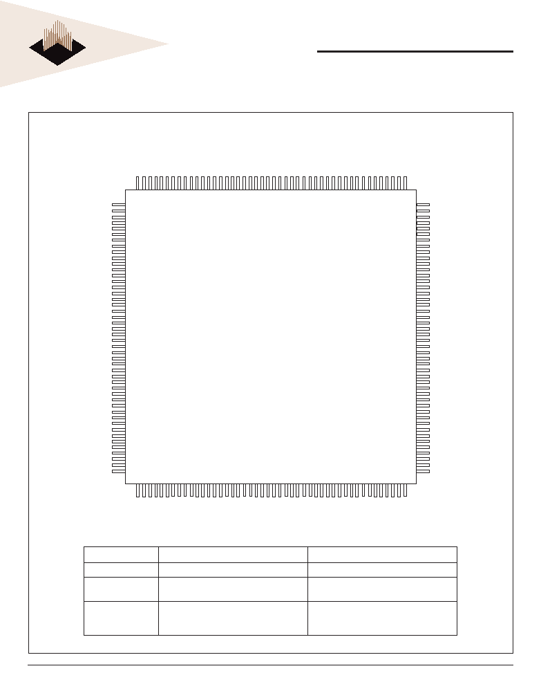
FIGURE 2 ≠
PIN CONFIGURATION FOR WC32P040-XXM, CQFP (Q4)
139
140
141
142
143
144
145
146
147
148
149
150
151
152
153
154
155
156
157
158
159
160
161
162
163
164
165
166
167
168
169
170
171
172
173
174
175
176
177
178
179
180
181
182
183
184
138
137
136
135
134
133
132
131
130
129
128
127
126
125
124
123
122
121
120
11
9
11
8
11
7
11
6
11
5
11
4
11
3
11
2
111
11
0
109
108
107
106
105
104
103
102
101
100
99
98
97
96
95
94
93
GND
GND
A
31
A
30
V
CC
A
29
A
28
GND
A
27
A
26
V
CC
A
25
A
24
GND
A
23
A
22
V
CC
A
21
A
20
GND
A
19
A
18
V
CC
GND
A
17
A
16
GND
A
15
A
14
V
CC
A
13
A
12
GND
A
11
A
10
GND
V
CC
TT
1
TT
0
GND
UPA
1
UPA
0
V
CC
CIOUT#
IPEND#
GND
RST
O#
TD
0
TD
1
TCK
GND
TRST#
TMS
GND
V
CC
MDIS#
CDIS#
RSTI#
IPL
2#
IPL
1#
IPL
0#
GND
GND
BCLK
V
CC
GND
V
CC
GND
PCLK
GND
GND
DLE
GND
GND
TCI#
A
VEC#
TBI#
V
CC
GND
SC
0
SC
1
BG#
TEA#
TA
#
PST
0
GND
PST
1
PST
2
V
CC
PST
3
TIP
GND
D
27
GND
D
28
D
29
V
CC
D
30
D
31
GND
GND
A
9
A
8
V
CC
A
7
A
6
GND
A
5
A
4
V
CC
A
3
A
2
GND
A
1
A
0
V
CC
GND
TM
2
TM
1
GND
TM
0
TLN
1
V
CC
TLN
0
SIZ
0
GND
R/W#
LOCKE#
V
CC
GND
SIZ
1
LOCK#
GND
MI#
BR#
V
CC
TS#
BB#
D
0
D
1
V
CC
GND
D
2
D
3
GND
D
4
GND
D
5
V
CC
D
6
D
7
GND
D
8
D
9
V
CC
GND
D
10
D
11
GND
D
12
D
13
V
CC
D
14
D
15
GND
D
16
D
17
V
CC
GND
D
18
D
19
GND
D
20
D
21
V
CC
D
22
V
CC
D
23
GND
D
24
D
25
GND
V
CC
D
26
1
2
3
4
5
6
7
8
9
10
11
12
13
14
15
16
17
18
19
20
21
22
23
24
25
26
27
28
29
30
31
32
33
34
35
36
37
38
39
40
41
42
43
44
45
46
92
91
90
89
88
87
86
85
84
83
82
81
80
79
78
77
76
75
74
73
72
71
70
69
68
67
66
65
64
63
62
61
60
59
58
57
56
55
54
53
52
51
50
49
48
47
TOP VIEW
Pin Group
GND
Vcc
PLL
17, 22, 24
19, 21
Internal Logic
5, 8, 10, 27, 28, 33, 55, 68, 95, 108, 121, 130,
135, 162, 174
9, 32, 56, 69, 81, 94, 100, 109, 122, 136, 149,
161, 175
Output Drivers
16, 20, 25, 40, 46, 52, 59, 65, 72, 78, 84, 85,
91, 98, 105, 112, 118, 125, 132, 139, 140, 146,
152, 158, 165, 171, 178, 184
43, 49, 62, 75, 88, 102, 115, 128, 143, 155,
168, 181

3
White Electronic Designs Corporation ∑ (602) 437-1520 ∑ www.wedc.com
White Electronic Designs
WC32P040-XXM
July 1998
FIGURE 3 ≠
PIN CONFIGURATION FOR WC32P040-XXM, PGA (P4)
IPEND#
CIOUT#
UPA
1
A
10
A
12
A
13
A
14
A
15
A
17
A
18
A
20
A
21
A
22
A
24
A
27
A
29
A
31
1 2 3 4 5 6 7 8 9 10 11 12 13 14 15 16 17 18
TDO
GND
V
CC
GND
TT1
GND
V
CC
GND
A
16
A
19
GND
V
CC
GND
A
26
GND
V
CC
GND
D
3
TRST#
TDI
RTSO#
UPA
0
TT
0
A
11
V
CC
GND
GND
V
CC
V
CC
A
23
A
25
A
28
A
30
D
0
D
1
D
4
GND
TCK
GND
D
2
GND
D
5
CDIS#
TMS
V
CC
V
CC
V
CC
D
6
IPL
2
#
MDIS#
GND
GND
GND
D
7
IPL
1
#
RSTI#
BCLK
GND
D
8
D
9
IPL
0
#
V
CC
V
CC
V
CC
GND
D
10
DLE
GND
PCLK
GND
V
CC
D
11
TCI#
GND
GND
V
CC
GND
D
12
AVEC#
TBI#
GND
GND
D
16
D
13
BB#
GND
V
CC
GND
SIZ
0
GND
V
CC
GND
TM
2
A
2
GND
V
CC
GND
D
30
GND
V
CC
GND
D
21
BR#
LOCK#
LOCKE#
TLN
0
TLN
1
TM
0
TM
1
A
0
A
1
A
3
A
4
A
5
A
7
A
8
D
31
D
28
D
26
D
24
T
S
R
Q
P
N
M
L
K
J
H
G
F
E
D
C
B
A
V
CC
D
18
D
14
GND
GND
D
15
V
CC
V
CC
D
17
D
23
GND
D
19
PST
3
V
CC
TS#
MI#
SIZ
1
R/W#
GND
V
CC
GND
V
CC
V
CC
A
6
A
9
D
29
D
27
D
25
D
22
D
20
SC
0
SC
1
V
CC
BG#
TEA#
GND
TA#
PST
1
PST
2
PST
0
GND
TIP#
BOTTOM VIEW
Pin Group
GND
Vcc
PLL
S9, R6, R10
R8, S8
Internal Logic
C6, C7, C9, C11, C13, K3, L3, M16, R4, R11,
R13, S6, S10, T4
C5, C8, C10, C12, C14, H3, H16, J3, J16,
L16, M3, R5, R12
Output Drivers
B2, B4, B6, B8, B10, B13, B15, B17, D2, D17,
F2, F17, H2, H17, L2, L17, N2, N17, Q2, Q17,
S2, S15, S17
B5, B9, B14, C2, C17, G2, G17, M2, M17, R2,
R17, S16

4
White Electronic Designs Corporation ∑ (602) 437-1520 ∑ www.wedc.com
White Electronic Designs
WC32P040-XXM
July 1998
ADDRESSSING
The WC32P040 supports the basic addressing modes of
the 68000 family. The register indirect addressing modes
support postincrement, predecrement, offset, and indexing.
The program counter indirect mode also has indexing and
offset capabilities.
ADDRESSING MODES
Addressing
Syntax
Register Direct
Data Register Direct
Address Register Direct
Dn
An
Register Indirect
Address Register Indirect
Address Register Indirect with Postincrement
Address Register Indirect with Predecrement
Address Register Indirect with Displacement
(An)
(An) +
- (An)
(d16,An)
Register Indirect with Index
Address Register Indirect with Index (8-Bit Displacement)
Address Register Indirect with Index (Base Displacement)
(d8,An,Xn)
(bd,An,Xn)
Memory Indirect
Memory Indirect Postindexed
Memory Indirect Preindexed
([bd,An],Xn,od)
([bd,An,Xn],od)
Program Counter Indirect with Displacement
(d16,PC)
Program Counter Indirect with Index
PC Indirect with Index (8-Bit Displacement)
PC Indirect with Index (Base Displacement)
(d8,PC,Xn)
(bd,PC,Xn)
Program Counter Memory Indirect
PC Memory Indirect Postindexed
PC Memory Indirect Preindexed
([bd,PC],Xn,od)
([bd,PC,Xn],od)
Absolute
Absolute Short
Absolute Long
(xxx).W
(xxx).L
Immediate
#<xxx>
INSTRUCTION SET SUMMARY
Opcode
Operation
Syntax
ABCD
BCD Source + BCD Destination + X Destination
ABCD Dy,Dx
ABCD -(Ay),-(Ax)
ADD
Source + Destination Destination
ADD <ea>,Dn
ADD Dn,<ea>
ADDA
Source + Destination Destination
ADDA <ea>,An
ADDI
Immediate Data + Destination Destination
ADDI #<data>,<ea>
ADDQ
Immediate Data + Destination Destination
ADDQ #<data>,<ea>
ADDX
Source + Destination + X Destination
ADDX Dy,Dx
ADDX -(Ay),-(Ax)
AND
Source
Destination Destination
AND <ea>,Dn
AND Dn,<ea>
ANDI
Immediate Data
Destination Destination
ANDI #<data>,<ea>
ANDI to CCR
Source
CCR CCR
ANDI #<data>,CCR
ANDI to SR
If supervisor state
then
Source
SR SR
else TRAP
ANDI #<data>,SR
DATA FORMATS
The WC32P040 supports the basic data formats of the
68000 family. Some data formats apply only to the IU,
some only to the FPU, and some to both. In addition, the
instruction set supports operations on other data formats
such as memory addresses.
DATA FORMATS
Operand Data
Format
Size
Supported In
Notes
Bit
1 Bit
IU
--
Bit Field
1-32 Bits
IU
Field of Consecutive Bits
Binary-Coded
Decimal (BCD)
8 Bits
IU
Packed: 2 Digits/Byte;
Unpacked: 1 Digit/Byte
Byte Integer
8 Bits
IU, FPU
--
Word Integer
16 Bits
IU, FPU
--
Long-Word Integer
32 Bits
IU, FPU
--
Quad-Word Integer
64 Bits
IU
Any Two Data Registers
16-Byte
128 Bits
IU
Memory Only, Aligned to
16-Byte Boundary
Single-Precision Real
32 Bits
FPU
1-Bit Sign, 8-Bit Exponent,
23-Bit Fraction
Double-Precision
Real
64 Bits
FPU
1-Bit Sign,11-Bit
Exponent, 52-Bit Fraction
Extended-Precision
Real
80 Bits
FPU
1-Bit Sign,15-Bit
Exponent, 64-Bit Mantissa

5
White Electronic Designs Corporation ∑ (602) 437-1520 ∑ www.wedc.com
White Electronic Designs
WC32P040-XXM
July 1998
Opcode
Operation
Syntax
ASL,ASR
Destination Shifted by count Destination
ASd Dx,Dy
(1)
ASd #<data>,Dy
(1)
ASd <ea>
(1)
Bcc
It condition true
then PC + dn PC
Bcc <label>
BCHG
~(bit number of Destination) Z;
~(bit number ot Destination) (bit number) of Destination
BCHG Dn,<ea>
BCHG #<data>,<ea>
BCLR
~(bit number ot Destination) Z;
0 bit number ot Destination
BCLR Dn,<ea>
BCLR #<data>,<ea>
BFCHG
~(bit fi eld ot Destination) bit fi eld of Destination
BFCHG <ea> {offset:width}
BFCLR
0 bit fi eld of Destination
BFCLR <ea> {offset:width}
BFEXTS
bit fi eld of Source Dn
BFEXTS <ea> {offset:width}, Dn
BFEXTU
bit offset of Source Dn
BFEXTU <ea> {offset:width}, Dn
BFFFO
bit offset of Source Bit Scan Dn
BFFFO <ea> {offset:width}, Dn
BFINS
Dn bit fi eld of Destination
BFINS Dn,<ea> {offset:width}
BFSET
1s bit fi eld of Destination
BFSET <ea> {offset:width}
BFTST
bit fi eld of Destination
BFTST <ea> {offset:width}
BKPT
Run breakpoint acknowledge cycle; TRAP as illegal instruction
BKPT #<data>
BRA
PC+dn PC
BRA <label>
BSET
~(bit number ot Destination) Z;
1 bit number of Destination
BSET Dn,<ea>
BSET #<data>,<ea>
BSR
SP - 4 SP; PC (SP); PC + dn PC
BSR <label>
BTST
≠(bit number of Destination) Z
BTST Dn,<ea>
BTST #<data>,<ea>
CAS
CAS Destination ≠ Compare Operand cc;
if Z, Update Operand Destination
else Destination Compare Operand
CAS Dc,Du,<ea>
CAS2
CAS2 Destination 1 ≠ Compare 1 cc;
if Z, Destination 2 ≠ Compare cc;
if Z, Update 1 Destination 1;
Update
2 Destination 2
else Destination 1 Compare 1;
Destination
2 Compare 2
CAS2 Dc1-Dc2,Du1-Du2,(Rn1)-(Rn2)
CHK
If Dn < 0 or Dn > Source then TRAP
CHK <ea>,Dn
CHK2
If Rn < LB or If Rn > UB then TRAP
CHK2 <ea>,Rn
CINV
If supervisor state
then invalidate selected cache lines
else TRAP
CINVL <caches>,
(An) CINVP <caches>,
(An) CINVA <caches>
CLR
0 Destination
CLR <ea>
CMP
Destination ≠ Source cc
CMP <ea>,Dn
CMPA
Destination ≠ Source
CMPA <ea>,An
CMPI
Destination ≠ Immediate Data
CMPI #<data>,<ea>
CMPM
Destination ≠ Source cc
CMPM (Ay)+,(Ax)+
CMP2
Compare Rn < LB or Rn > UB and Set Condition Codes
CMP2 <ea>,Rn
CPUSH
If supervisor state
then it data cache push selected dirty data cache lines;
invalidate selected cache lines
else TRAP
CPUSHL <caches>, (An)
CPUSHP <caches>, (An)
CPUSHA <caches>
INSTRUCTION SET SUMMARY (contd)

6
White Electronic Designs Corporation ∑ (602) 437-1520 ∑ www.wedc.com
White Electronic Designs
WC32P040-XXM
July 1998
Opcode
Operation
Syntax
DBcc
If condition false
then (Dn-1 Dn;
if (Dn -1
then PC + dn PC)
DBcc Dn,<label>
DIVS, DIVSL
Destination + Source Destination
DIVS.W <ea>,Dn
DIVS.L <ea>,Dq
DIVS.L <ea>,Dr:Dq
DIVSL.L <ea>,Dr:Dq
32 + 16 16r:16q
32 + 32 32q
64 + 32 32r:32q
32 + 32 32r:32q
DIVU, DIVUL
Destination + Source Destination
DIVU.W <ea>,Dn
DIVU.L <ea>,Dq
DIVU.L <ea>,Dr:Dq
DIVUL.L <ea>,Dr:Dq
32 + 16 16r:16q
32 + 32 32q
64 + 32 32r:32q
32 + 32 32r:32q
EOR
Source
Destination Destination
EOR Dn,<ea>
EORI
Immediate Data
Destination Destination
EORI #<data>,<ea>
EORI to CCR
Source
CCR CCR
EORI #<data>,CCR
EORI to SR
If supervisor state
EORI #<data>,SR
then Source SR SR
else TRAP
EXG
Rx
Ry
EXG Dx,Dy
EXG Ax,Ay
EXG Dx,Ay
EXG Ay,Dx
EXT,EXTB
Destination Sign ≠ Extended Destination
EXT.W Dn
EXT.L L Dn
EXTB.L Dn
extend byte to word
extend word to long word
extend byte to long word
FABS
Absolute Value of Source FPn
FABS.<fmt> <ea>,FPn
FABS.X FPm,FPn
FABS.X FPn
FrABS.<fmt> <ea>,FPn
(2)
FrABS.X FPm,FPn
(2)
FrABS.X FPn
(3)
FADD
Source + FPn FPn
FADD.<fmt, <ea>,FPn
FADD.X FPm,FPn
FrADD.<fmt> <ea>,FPn
(2)
FrADD.X FPm,FPn
(2)
FBcc
If condition true
then PC + dn PC
FBcc.SIZE <label>
FCMP
FPn ≠ Source
FCMP.<fmt> <ea>,FPn
FCMP.X FPm,FPn
FDBcc
It condition true
then no operation
else Dn-1 Dn
if Dn -1
then PC + dn PC
else execute next instruction
FDBcc Dn,<label>
FDIV
FPn + Source FPn
FDIV.<tmt> <ea>,FPn
FDIV.X FPm,FPn
FrDIV.<fmt> <ea>,FPn
(2)
FrDIV.X FPm,FPn
(2)
FMOVE
Source Destination
FMOVE.<fmt> <ea>,FPn
FMOVE.<fmt> FPM,<ea>
FMOVE.P FPm,<ea>{Dn}
FMOVE.P FPm,<ea>{#k}
FrMOVE.<fmt> <ea>,FPn
(2)
INSTRUCTION SET SUMMARY (contd)

7
White Electronic Designs Corporation ∑ (602) 437-1520 ∑ www.wedc.com
White Electronic Designs
WC32P040-XXM
July 1998
Opcode
Operation
Syntax
FMOVE
Source Destination
FMOVE.L <ea>,FPcr
FMOVE.L FPcr,<ea>
FMOVEM
Register List Destination
Source Register List
FMOVEM.X <list>,<ea>
(3)
FMOVEM.X Dn,<ea>
FMOVEM.X <ea>,<list>
(3)
FMOVEM.X <ea>,Dn
FMOVEM
Register List Destination
Source Register List
FMOVEM.L <list>,<ea>
(4)
FMOVEM.L <ea>,<list>
(4)
FMUL
Source x FPn FPn
FMUL.<fmt> <ea>,FPn
FMUL.X FPm,FPn
FrMUL<fmt> <ea>,FPn
(2)
FrMUL.X FPm,FPn
(3)
FNEG
≠(Source) FPn
FNEG.<fmt> <ea>,FPn
FNEG.X FPm,FPn
FNEG.X FPn
FrNEG.<fmt> <ea>,FPn
(2)
FrNEG.X FPm,FPn
(2)
FrNEG.X FPn
(2)
FNOP
None
FNOP
FRESTORE
If in supervisor state
then FPU State Frame Internal State
else TRAP
FRESTORE <ea>
FSAVE
If in supervisor state
then FPU Internal State State Frame
else TRAP
FSAVE <ea>
FScc
If condition true
then 1s Destination
else 0s Destination
FScc.SIZE <ea>
FSGLDIV
FPn
˜ Source FPn
FSGLDIV.<fmt> <ea>,FPn
FSGLDIV.X FPm,FPn
FSGLMUL
Source x FPn FPn
FSGMUL.<tmt> <ea>,FPn
FSGLMUL.X FPm, FPn
FSQRT
Square Root of Source FPn
FSQRT.<fmt> <ea>,FPn
FSQRT.X FPm,FPn
FSQRT.X FPn
FrSQRT.<fmt> <ea,,FPn
(2)
FrSQRT FPm,FPn
(2)
FrSQRT FPn
(2)
FSUB
FPn ≠ Source FPn
FSUB.<fmt> <ea>,FPn
FSUB.X FPm,FPn
FrSUB.<tmt> <ea>,FPn
(2)
FrSUB.X FPm,FPn3
(2)
FTRAPcc
If condition true
then TRAP
FTRAPcc
FTRAPcc.W #<data>
FTRAPcc.L #<data>
FTST
Condition Codes tor Operand FPCC
FTST.dmt> <ea>
FTST.X FPm
ILLEGAL
SSP ≠ 2 SSP; Vector Offset (SSP);
SSP ≠ 4 SSP; PC (SSP);
SSp ≠ 2 SSP; SR (SSP)
Illegal Instruction Vector Address PC
ILLEGAL
JMP
Destination Address
PC
JMP <ea>
INSTRUCTION SET SUMMARY (contd)

8
White Electronic Designs Corporation ∑ (602) 437-1520 ∑ www.wedc.com
White Electronic Designs
WC32P040-XXM
July 1998
JSR
SP ≠ 4 SP; PC (SP)
Destination Address
PC
JSR <ea>
Opcode
Operation
Syntax
LEA
<ea> An
LEA <ea>,An
LINK
SP ≠ 4 SP;An (SP)
SP An, SP + d SP
LINK An,dn
LSL,LSR
Destination Shifted by count Destination
LSd Dx,Dy
(1)
LSd #<data>,Dy
(1)
LSd <ea>
(1)
MOVE
Source Destination
MOVE <ea>,<ea>
MOVEA
Source Destination
MOVEA <ea>, An
MOVE from CCR
CCR Destination
MOVE CCR,<ea>
MOVE to CCR
Source CCR
MOVE <ea>,CCR
MOVE from SR
If supervisor state
then SR Destination
else TRAP
MOVE SR,<ea>
MOVE to SR
If supervisor state
then Source SR
else TRAP
MOVE <ea>,SR
MOVE USP
It supervisor state
then USP An or An
USP
else TRAP
MOVE USP,An
MOVE An,USP
MOVE1 6
Source block Destination block
MOVE16 (Ax)+, (Ay)+
(5)
MOVE16 (xxx).L, (An)
MOVE16 (An), (xxx).L
MOVE16 (An)+, (xxx).L
MOVEC
If supervisor state then Rc Rn or Rn Rc else TRAP
MOVEC Rc,Rn
MOVEC Rn,Rc
MOVEM
Registers Destination
Source Registers
MOVEM <list>,<ea>
(3)
MOVEM <ea>,<list>
(3)
MOVEP
Source Destination
MOVEP Dx,(dn,Ay)
MOVEP (dn,Ay),Dx
MOVEQ
Immediate Data Destination
MOVEQ #<data>,Dn
MOVES
If supervisor state
then Rn Destination [DFC) or Source [SFC] Rn
else TRAP
MOVES Rn,<ea>
MOVES <ea>,Rn
MULS
Source x Destination Destination
MULS.W <ea>,Dn
MULS.L <eai,Dl
MULS.L <ea>,Dh-Dl
16 x 16 32
32 x 32 32
32 x 32 64
MULU
Source x Destination Destination
MULU.W <ea>,Dn
MULU.L <ea>,DI
MULU.L <ea>,Dh-DI
16 x 16 32
32 x 32 32
32 x 32 64
NBCD
0 ≠ (Destination10) ≠ X Destination
NBCD <ea>
NEG
0 ≠ (Destination) Destination
NEG <ea>
NEGX
0 ≠ (Destination) ≠ X Destination
NEGX <ea>
NOP
None
NOP
NOT
~ Destination Destination
NOT <ea>
OR
Source V Destination Destination
OR <ea>,Dn
OR Dn,<ea>
INSTRUCTION SET SUMMARY (contd)

9
White Electronic Designs Corporation ∑ (602) 437-1520 ∑ www.wedc.com
White Electronic Designs
WC32P040-XXM
July 1998
Opcode
Operation
Syntax
ORI
Immediate Data V Destination Destination
ORI #<data>,<ea>
ORI to CCR
Source V CCR CCR
ORI #<data>,CCR
ORI to SR
If supervisor state
then Source V SR SR
else TRAP
ORI #<data>,SR
PACK
Source (Unpacked BCD) + adjustment Destination (Packed BCD)
PACK -(Ax),-(Ay),#(adjustment)
PACK Dx,Dy,#(adjustment)
PEA
SP ≠ 4 SP; <ea> (SP)
PEA <ea>
PFLUSH
If supervisor state
then invalidate instruction and data ATC entries
for destination address
else TRAP
PFLUSH (An)
PFLUSHN (An)
PFLUSHA
PFLUSHAN
PTEST
If supervisor state
then logical address status MMUSR; entry ATC
else TRAP
PTESTR (An)
PTESTW (An)
RESET
If supervisor state
then Assert RSTO# Line
else TRAP
RESET
ROL, ROR
Destination Rotated by count Destination
ROd Rx,Dy(1)
ROd #<data>,Dy(1)
ROXL, ROXR
Destination Rotated with X by count Destination
ROXd Dx,Dy(1)
ROXd #<data>,Dy(1)
ROXd <ea>(1)
RTD
(SP) PC; SP + 4 + dn SP
RTD #(dn)
RTE
If supervisor state
then (SP) SR; SP + 2 SP; (SP) PC; SP + 4 SP;
restore state and deallocate stack according to (SP)
else TRAP
RTE
RTR
(SP) CCR; SP + 2 SP;
(SP) PC; SP + 4 SP
RTR
RTS
(SP) PC; SP + 4 SP
RTS
SBCD
Destination10 ≠ Source10 ≠ X Destination
SBCD Dx,Dy
SBCD ≠(Ax),≠(Ay)
Scc
If condition true
then 1s Destination
else 0s Destination
Scc <ea>
STOP
If supervisor state
then Immediate Data SR; STOP
elseTRAP
STOP #<data>
SUB
Destination ≠ Source Destination
SUB <ea>,Dn
SUB Dn,<ea>
SUBA
Destination ≠ Source Destination
SUBA <ea>,An
SUBI
Destination ≠ Immediate Data Destination
SUBI #<data>,<ea>
SUBQ
Destination ≠ Immediate Data Destination
SUBQ #<data>,<ea>
INSTRUCTION SET SUMMARY (contd)

10
White Electronic Designs Corporation ∑ (602) 437-1520 ∑ www.wedc.com
White Electronic Designs
WC32P040-XXM
July 1998
Opcode
Operation
Syntax
SUBX
Destination ≠ Source ≠ X Destination
SUBX Dx,Dy
SUBX (Ax), (Ay)
SWAP
Register 31 ≠ 16 Register 15 ≠ 0
SWAP Dn
TAS
Destination Tested Condition Codes;
1 bit 7 of Destination
TAS <ea>
TRAP
SSP ≠ 2 SSP; Format + Offset (SSP)
SSP ≠ 4 SSP; PC (SSP); SSP - 2 SSP;
SR (SSP); Vector Address PC
TRAP #<vector>
TRAPcc
If cc
then TRAP
TRAPcc
TRAPcc.W #<data>
TRAPcc.L #<data>
TRAPV
If V
then TRAP
TRAPV
TST
Destination Tested Condition Codes
TST <ea>
UNLK
An SP; (SP) An; SP + 4 SP
UNLK An
UNPK
Source (Packed BCD) + adjustment Destination (Unpacked BCD)
UNPACK ≠(Ax ), ≠(Ay), # (adjustment)
UNPACK Dx,Dy, #(adjustment)
NOTES:
1. Where d is direction, left or right.
2. Where r is rounding precision, single or double precision.
3. List refers to register.
4. List refers to control registers only.
5. MOVE16 (ax)+, (ay)+ is functionally the same as MOVE16 (ax), (ay)+ when ax = ay.
The address register is only incremented once, and the line is copied over itself rather than to the next line.
INSTRUCTION SET SUMMARY (contd)

11
White Electronic Designs Corporation ∑ (602) 437-1520 ∑ www.wedc.com
White Electronic Designs
WC32P040-XXM
July 1998
FIGURE 4 ≠ FUNCTIONAL SIGNAL GROUPS
A31-A0
D31-D0
TT0
TT1
TM0
TM1
TM2
TLN0
TLN1
UPA0
UPA1
R/W
SIZ0
SIZ1
LOCK
LOCKE
CIOUT
TS
TIP
TA
TEA
TCI
TBI
DLE
SC0
SC1
MI#
BR#
BG#
BB#
CDIS#
MDIS#
RSTI#
RSTO#
IPL0#
IPL1#
IPL2#
IPEND#
AVEC#
PST0
PST1
PST2
PST3
BCLK
PCLK
TCK
TMS
TDI
TDO
TRST#
Vcc
GND
TRANSFER
ATTRIBUTES
POWER SUPPLY
BUS SNOOP CONTROL
AND RESPONSE
BUS ARBITRATION
MASTER
TRANSFER
CONTROL
PROCESSOR
CONTROL
ADDRESS
BUS
DATA
BUS
SLAVE
TRANSFER
CONTROL
INTERRUPT
CONTROL
STATUS AND
CLOCKS
TEST

12
White Electronic Designs Corporation ∑ (602) 437-1520 ∑ www.wedc.com
White Electronic Designs
WC32P040-XXM
July 1998
SIGNAL INDEX
Signal Name
Mnemonic
Function
Address Bus
A31-A0
32-bit address bus used to address any of 4-Gbytes.
Data Bus
D31-D0
32-bit data bus used to transfer up to 32 bits of data per bus transfer.
Transfer Type
TT1,TT0
Indicates the general transfer type: normal, MOVE16, alternate logical function code, and acknowledge.
Transfer Modifi er
TM2-TM0
Indicates supplemental information about the access.
Transfer Line Number
TLN1-TLN0
Indicates which cache line in a set is being pushed or loaded by the current line transfer.
User-Progammable Attributes
UPA1,UPA0
User-defi ned signals, controlled by the corresponding user attribute bits from the address translation entry.
Read/Write
R/W#
Identifi es the transfer as a read or write.
Transfer Size
SIZ0/SIZ1
Indicates the data transfer size. These signals, together with A0 and A1, defi ne the active sections of the data
bus.
Bus Lock
LOCK#
Indicates a bus transfer is part of a read-modify-write operation, and the sequence of transfers should be
interrupted.
Bus Lock End
LOCKE#
Indicates the current transfer is the last in a locked sequence of transfers.
Cache Inhibit Out
CIOUT#
Indicates the processor will not cache the current bus transfer.
Transfer Start
TS#
Indicates the beginning of the bus transfer.
Transfer on Progress
TIP#
Asserted for the duration of a bus transfer.
Transfer Acknowledge
TA#
Asserted to acknowledge a bus transfer.
Transfer Error Acknowledge
TEA#
Indicates an error condition exists for a bus transfer.
Transfer Cache Inhibit
TCI#
Indicates the current bus transfer should not be cached.
Transfer Burst Inhibit
TBI#
Indicates the slave cannot handle a line burst access.
Data Latch Enable
DLE
Alternate clock input used to latch input data when the processor is operating in DLE mode.
Snoop Control
SC1,SC0
Indicates the snooping operation required during an alternate master access.
Memory Inhibit
MI#
Inhibits mem ory devices from responding to an alternate master access during snooping operations.
Bus Request
BR#
Asserted by the processor to request bus mastership.
Bus Grant
BG#
Asserted by an arbiter to grant bus mastership to the processor.
Bus Busy
BB#
Asserted by the current bus master to indicate it has assumed ownership of the bus.
Cache Disable
CDIS#
Dynamically disables the internal caches to assist emulator support.
MMU Disable
MDIS#
Disables the translation mechanism of the MMUs.
Reset In
RSTI#
Processor reset.
Reset Out
RSTO#
Asserted during execution of a RESET instruction to reset external devices.
Interrupt Priority Level
IPL2#-IPL0#
Provides an encoded interrupt level to the processor.
Interrupt Pending
IPEND#
Indicates an interrupt is pending.
Autovector
AVEC#
Used during an interrupt acknowledge transfer to request internal generation of the vector number.
Processor Status
PST3-PST0
Indicates internal processor status.
Processor Clock
PCLK
Clock input used for internal logic timing. The PCLK frequency is exactly 2 x the BLCK frequency.
Test Clock
TCK
Clock signal for the IEEE P1149.1 Test Access Port (TAP).
Test Mode Select
TMS
Selects the principle operations of the test-support circuitry.
Test Data Input
TDI
Serial data input for the TAP.
Test Data Output
TDO
Serial data output for the TAP.
Test Reset
TRST#
Provides an asynchronous reset of the TAP controller.
Power Supply
Vcc
Power supply.
Ground
GND
Ground connection.

13
White Electronic Designs Corporation ∑ (602) 437-1520 ∑ www.wedc.com
White Electronic Designs
WC32P040-XXM
July 1998
DC ELECTRICAL SPECIFICATIONS
V
CC
= 5.0 V
DC
± 5%
Characteristics
Symbol
Min
Max
Unit
Input High Voltage
VIH
2.0
Vcc
V
Input Low Voltage
VIL
GND
0.8
V
Undershoot
--
--
0.8
V
Input Leakage Current @ 0.5/2.4V
AVEC#, BCLK, BG#, CDIS#, MDIS#, IPLx#, PCLK, RSTI#, SCx,
TBI#, TMx, TLNx, TCI#, TCK, TEA#
IIN
20
20
µA
High-Z (Off State) Leakage Current @
0.5/2.4 V
An, BB#, CIOUT#, Dn, LOCK#, LOCKE#, R/W#, SIZX, TA#,
TDO, TIP#, TMx, TLNx, TS#, TTx, UPAx
ITSI
20
20
µA
Signal Low Input Current, VIL = 0.8V
TMS, TDI, TRST#
IIL
-1.1
-0.18
mA
Signal High Input Current, VIH = 2.0V
TMS, TDI, TRST#
IIH
-0.94
-0.16
mA
Output High Voltage, IOH = 5mA (Small Buffer Mode)
VOH
2.4
--
V
Output Low Voltage, IOL = 5mA (Small Buffer Mode)
VOL
--
0.5
V
Output High Voltage, IOH = 55mA (Large Buffer Mode)
VOH
2.4
--
V
Output Low Voltage, IOL = 55mA (Large Buffer Mode)
VOL
--
0.5
V
Capacitance (1), VIN = 0V, f = 1MHz
CIN
--
20
pF
NOTE: 1. Capacitance is guaranteed by design but not tested.
MAXIMUM RATINGS
Parameter
Symbol
Value
Unit
Supply Voltage
V
CC
-0.3 to +7.0
V
Input Voltage
V
IN
-0.5 to +7.0
V
Maximum Operating Temperature
T
J
+125
∞C
Minimum Operating Temperature
T
A
-55
∞C
Storage Temperature
T
STG
-55 to +150
∞C
THERMAL CHARACTERISTICS
Parameter
Symbol
Value
Rating
Thermal Resistance, Junction to
Case ≠ PGA Package
JC
3.0
∞C/W
POWER DISSIPATION
Buffer Mode
25 MHz
33 MHz
Small Unterminated, IOL = IOH = 5mA
4.9W
6.2W
Large Unterminated, IOL = IOH = 5mA
5.1W
6.6W
Large Terminated, 50 , 2.5V, IOL = IOH = 55mA
6.5W
8.0W
14
White Electronic Designs Corporation ∑ (602) 437-1520 ∑ www.wedc.com
White Electronic Designs
WC32P040-XXM
July 1998
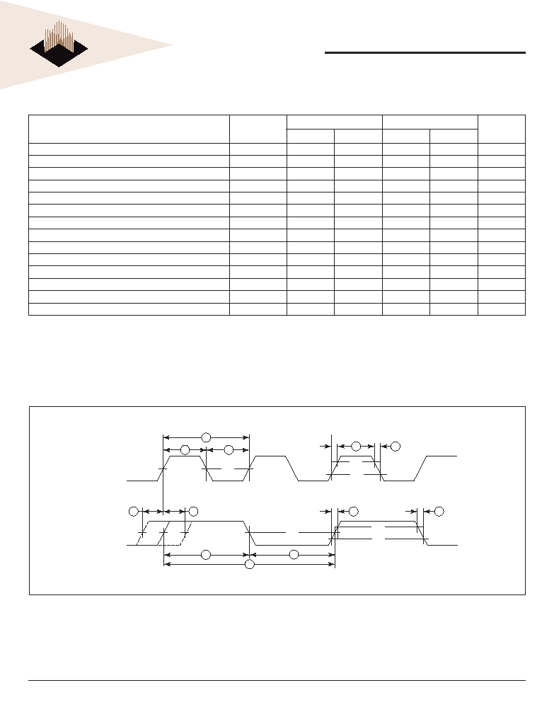
FIGURE 5 ≠ CLOCK INPUT TIMING DIAGRAM
CLOCK AC TIMING SPECIFICATIONS (SEE FIGURE 5)
Characteristic
Specifi cation
25 MHz
33 MHz
Unit
Min
Max
Min
Max
Frequency of Operation
20
25
20
33
MHz
PCLK Cycle Time
1
20
25
15
25
ns
PCLK Rise Time
2
--
1.7
--
1.7
ns
PCLK Fall Time
3
--
1.6
--
1.6
ns
PCLK Duty Cycle Measured at 1.5V
4
47.50
52.50
46.67
53.33
%
PCLK Pulse Width High Measured at 1.5V
4A (1)
9.50
10.50
7
8
ns
PCLK Pulse Width Low Measured at 1.5V
4B (1)
9.50
10.50
7
8
ns
BCLK Cycle Time
5
40
50
30
50
ns
BCLK Rise and Fall Time
6,7
--
4
--
3
ns
BCLK Duty Cycle Measured at 1.5V
8
40
60
40
60
%
BCLK Pulse Width High Measured at 1.5V
8A (1)
16
24
12
18
ns
BCLK Pulse Width Low Measured at 1.5V
8B (1)
16
24
12
18
ns
PCLK, BCLK Frequency Stability
9
--
1000
--
1000
ppm
PCLK and BCLK Skew
10
--
9
--
n/a
ns
NOTES: 1. Specifi cation value at maximum frequency of operation.
1
V
M
V
M
V
il
V
iH
V
iH
PCLK
BCLK
4A
10
10
6
7
8A
5
8B
4B
V
IL
2
3

15
White Electronic Designs Corporation ∑ (602) 437-1520 ∑ www.wedc.com
White Electronic Designs
WC32P040-XXM
July 1998
OUTPUT AC TIMING SPECIFICATIONS (SEE FIGURE 6-10)
Characteristic
Specifi cation
25 MHz
33 MHz
Unit
Large (1)
Small (2)
Large (1)
Small (2)
Min
Max
Min
Max
Min
Max
Min
Max
BCLK to Address CIOUT#, LOCK#, LOCKE#, R/W#, SIZx,
TLN, TMx, TTx, UPAx Valid
11 (3)
9
21
9
30
6.50
18
6.50
25
ns
BCLK to Output Invalid (Output Hold)
12
9
≠
9
≠
6.50
≠
6.50
≠
ns
BCLK to TS# Valid
13
9
21
9
30
6.50
18
6.50
25
ns
BCLK to TIP# Valid
14
9
21
9
30
6.50
18
6.50
25
ns
BCLK to Data Out Valid
18 (4)
9
23
9
32
6.50
20
6.50
27
ns
BCLK to Data Out Invalid (Output Hold)
19 (4)
9
≠
9
≠
6.50
≠
6.50
≠
ns
BCLK to Output Low Inpedance
20 (3,4)
9
≠
9
≠
6.50
≠
6.50
≠
ns
BCLK to Data-Out High Impedance
21 (5)
9
20
9
20
6.50
17
6.50
17
ns
BCLK to Multiplexed Address Valid
26 (3)
19
31
19
40
14
26
14
33
ns
BCLK to Multiplexed Address Driven
27 (3,5)
19
≠
19
≠
14
≠
14
≠
ns
BCLK to Multiplexed Address High Impedance
28 (3,4,5)
9
18
9
18
6.50
15
6.50
15
ns
BCLK to Multiplexed Data Valid
29 (4,5)
19
≠
19
≠
14
20
14
20
ns
BCLK to Multiplexed Data Driven
30 (4)
19
33
19
42
14
28
14
35
ns
BCLK to Address, CIOUT#, LOCK#, LOCKE#, R/W#, SIZx,
TS#, TLNx, TMx, TTx, UPAx High Impedance
38 (3)
9
18
9
18
6.50
15
6.50
15
ns
BLCLK to BB#, TA#, TIP# High Impedance
39
19
28
19
28
14
23
14
23
ns
BCLK to BR#, BB# Valid
40
9
21
9
30
6.50
18
6.50
25
ns
BCLK to MI# Valid
43
9
21
9
30
6.50
18
6.50
25
ns
BCLK to TA# Valid
48
9
21
9
30
6.50
18
6.50
25
ns
BCLK to IPEND#, PSTx, RSTO# Valid
50
9
21
9
30
6.50
18
6.50
25
ns
NOTES:
1.
Output timing is specifi ed for a valid signal measured at the pin. Large buffer timing
is specifi ed driving a 50
transmission line with a length characterized by a 2.5ns
one-way propagation delay, terminated through 50
to 2.5V. Large buffer output
impedance is 4-12
, resulting in incident wave switching for this environment. All
large buffer outputs must be terminated to guarantee operation.
2.
Small buffer timing is specifi ed driving an unterminated 30
transmission line with
a length characterized buy a 2.5ns one-way propagation delay. Small buffer output
impedance is typically 30
; the small buffer specifi cations include approximately
5ns for the signal to propagate the length of the transmission line and back.
3.
Timing specifi cations 11, 20, and 38 for address bus output timinng apply when
normal bus operation is selected. Specifi cations 26, 27, and 28 should be used
when the multiplexed bus mode of operation is enabled.
4.
Timing specifi cations 18 and 19 for data bus output timing apply when normal
bus operation is selected. Specifi cations 28 and 29 should be used when the
multiplexed bus mode of operation is enabled.
5.
Timing specifi cations 21, 27, 28, and 29 are measured from BCLK edges. By
design, the 68040 cannot drive address and data simultaneously during multiplexed
operations.

16
White Electronic Designs Corporation ∑ (602) 437-1520 ∑ www.wedc.com
White Electronic Designs
WC32P040-XXM
July 1998
INTPUT AC TIMING SPECIFICATIONS (SEE FIGURE 6-10)
Characteristic
Specifi cation
25 MHz
33 MHz
Unit
Min
Max
Min
Max
Data-In Valid to BCLK (Setup)
15
5
≠
4
≠
ns
BCLK to Data-In Valid (Hold)
16
4
≠
4
≠
ns
BCLK to Data-In High Impedance (Read Followed by Write)
17
≠
49
≠
36.5
ns
TA# Valid to BCLK (Setup)
22A
10
≠
10
≠
ns
TEA# Valid to BCLK (Setup)
22B
10
≠
10
≠
ns
TCI# Valid to BCLK (Setup)
22C
10
≠
10
≠
ns
TBI# Valid to BCLK (Setup)
22D
11
≠
10
≠
ns
BCLK to TA#, TEA#, TCI#, TBI# Invalid (Hold)
23
2
≠
2
≠
ns
AVEC# Valid to BCLK (Setup)
24
5
≠
5
≠
ns
BCLK to AVEC# Invalid (Hold)
25
2
≠
2
≠
ns
DLE Width High
31
8
≠
8
≠
ns
Data-In Valid to DLE (Setup)
32
2
≠
2
≠
ns
DLE to Data-In Invalid (Hold)
33
8
≠
8
≠
ns
BCLK to DLE Hold
34
3
≠
3
≠
ns
DLE High to BCLK
35
16
≠
12
≠
ns
Data-In Valid to BCLK (DLE Mode Setup)
36
5
≠
5
≠
ns
BCLK to Data-In Invalid (DLE Mode Hold)
37
4
≠
4
≠
ns
BB# Valid to BCLK (Setup)
41A
7
≠
7
≠
ns
BG# Valid to BCLK (Setup)
41B
8
≠
7
≠
ns
CDIS#, MDIS# Valid to BCLK (Setup)
41C
10
≠
8
≠
ns
IPLx# Valid to BCLK (Setup)
41D
4
≠
3
≠
ns
BCLK to BB#, BG#, CDIS#, IPLx#, MDIS# Invalid (Hold)
42
2
≠
2
≠
ns
Address Valid to BCLK (Setup)
44A
8
≠
7
≠
ns
SIZx Valid BCLK (Setup)
44B
12
≠
8
≠
ns
TTx Valid to BCLK (Setup)
44C
6
≠
8.5
≠
ns
R/W Valid to BCLK (Setup)
44D
6
≠
5
≠
ns
SCx Valid to BCLK (Setup)
44E
10
≠
11
≠
ns
BCLK to Address, SIZx, TTx, R/W#, SCx Invalid (Hold)
45
2
≠
2
≠
ns
TS# Valid to BCLK (Setup)
46
5
≠
9
≠
ns
BCLK to TS# Invalid (Hold)
47
2
≠
2
≠
ns
BCLK to BB# High Impedance (MC68040 Assumes Bus Mastership)
49
≠
9
≠
9
ns
RSTI# Valid to BCLK
51
5
≠
4
≠
ns
BCLK to RSTI# Invalid
52
2
≠
2
≠
ns
Mode Select Setup to RSTI# Negated
53
20
≠
20
≠
ns
RSTI# Negated to Mode Selects Invalid
54
2
≠
2
≠
ns
17
White Electronic Designs Corporation ∑ (602) 437-1520 ∑ www.wedc.com
White Electronic Designs
WC32P040-XXM
July 1998
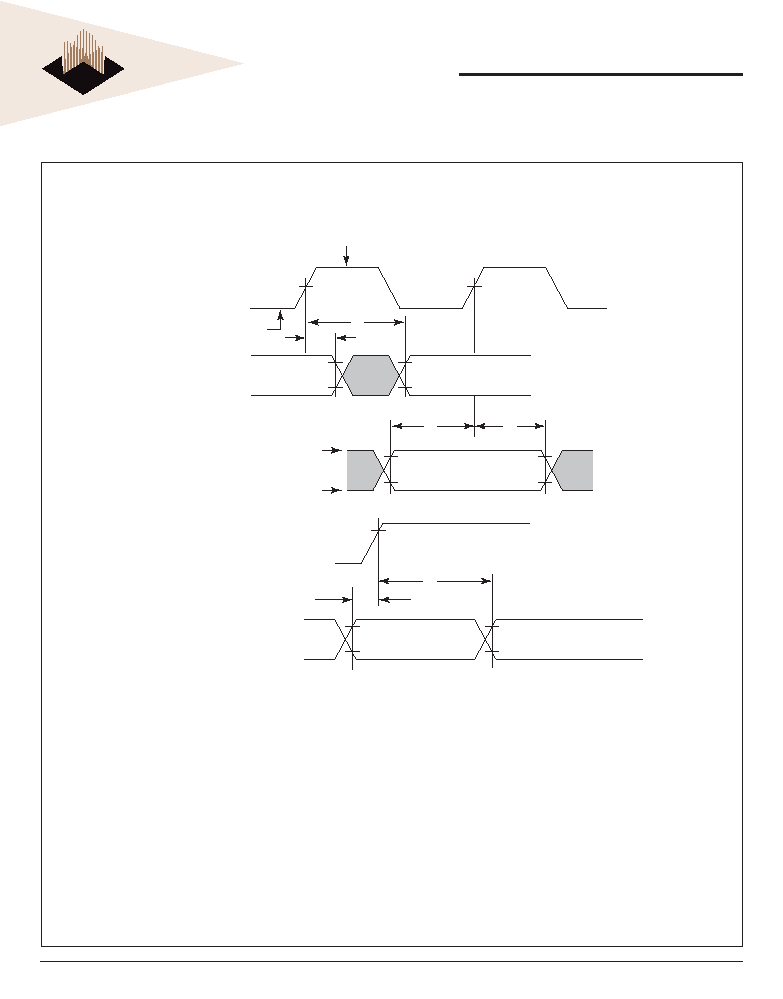
NOTE:
1.
This output timing is applicable to all parameters specifi ed relative to the rising edge of the clock.
2.
This input timing is applicable to all parameters specifi ed relative to the rising edge of the clock.
3.
This timing is applicable to all parameters specifi ed relative to the negation of the RSTI# signal.
LEGEND:
A. Maximum output delay specifi cation.
B. Minimum output hold time.
C. Minimum input setup time specifi cation.
D. Minimum input hold time specifi cation.
E. Mode select setup time to RSTI# negated.
F.
Mode select hold time to RSTI# negated.
FIGURE 6 ≠ DRIVE LEVELS AND TEST POINTS FOR AC SPECIFICATONS
2.0V
0.8V
2.0V
0.8V
2.0V
2.0V
F
D
C
B
A
VALID
INPUT
DRIVE TO
2.4V
DRIVE TO
0.5V
DRIVE TO
0.5V
BCLK
OUTPUTS (1)
INPUTS (2)
RSTI# (3)
IPLX#, CDIS#,
MDIS#
E
0.8V
2.0V
0.8V
2.0V
1.5V
1.5V
TO 2.4V
0.8V
VALID
OUTPUT
VALID
OUTPUT
n + 1
n

18
White Electronic Designs Corporation ∑ (602) 437-1520 ∑ www.wedc.com
White Electronic Designs
WC32P040-XXM
July 1998
FIGURE 7 ≠ READ/WRITE TIMING DIAGRAM
NOTE:
Transfer Attribute Signals = UPAx, SIZx, TTx, TMx, TLNx, R/W#, LOCK#, LOCKE#, CIOUT#
BCLK
A31-A0
TRANSFER
ATTRIBUTES
TS#
TIP#
TA#
TEA#
TCI#
AVEC#
TBI#
D31-D0 IN
(READ)
D31-D0 OUT
(WRITE)
11
12
12
12
13
14
18
20
22
15
21
19
16
23
24
25
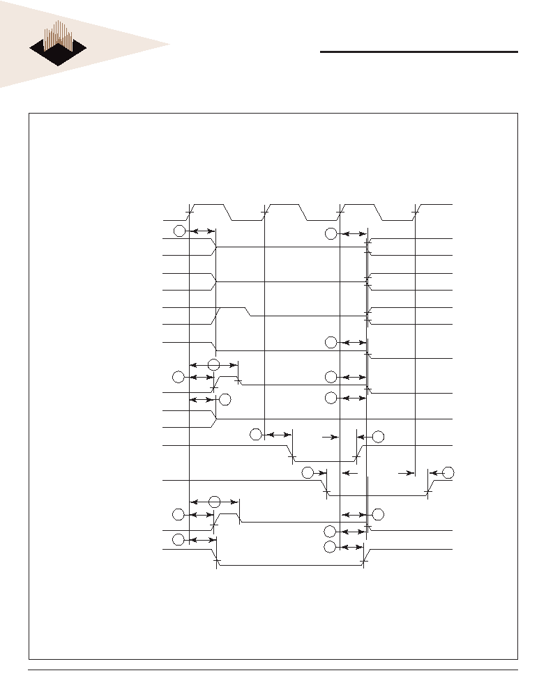
19
White Electronic Designs Corporation ∑ (602) 437-1520 ∑ www.wedc.com
White Electronic Designs
WC32P040-XXM
July 1998
FIGURE 8 ≠ BUS ARBITRATION TIMING DIAGRAM
NOTE: Transfer Attribute Signals = UPAx, SIZx, TTx, TMx, TLNx, R/W#, CIOUT#
38
BCLK
A31-A0
TRANSFER
ATTRIBUTES
LOCK#, LOCKE#
TS#
TIP#
BR#
BG#
MI#
BB OUT#
D31-D0 OUT
(WRITE)
11
13
14
12
39
39
21
20
40
40
12
43
20
12
12
42
41
20
White Electronic Designs Corporation ∑ (602) 437-1520 ∑ www.wedc.com
White Electronic Designs
WC32P040-XXM
July 1998
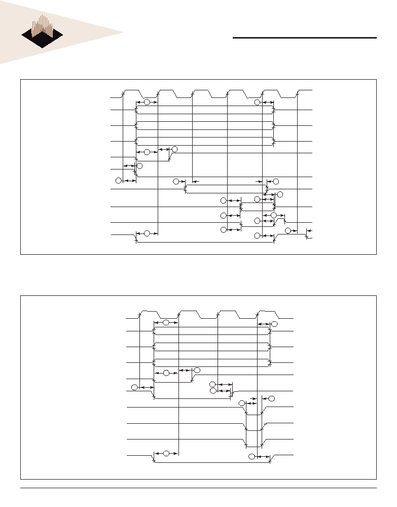
FIGURE 9 ≠ SNOOP HIT TIMING DIAGRAM
FIGURE 10 ≠ SNOOP MISS TIMING DIAGRAM
43
43
23
47
45
12
42
22
44
46
41
BCLK
SNOOP
A31-A0 IN
SIZx, TTx,
R/W# IN
SC1, SC0
TS# IN
MI#
BB# IN
TA#
TEA#
TBI#
49
12
21
43
15
15
47
45
19
12
42
18
20
48
44
46
41
39
BCLK
A31-A0 IN
SIZx, TTx,
R/W# IN
SC1, SC0
TS# IN
MI
TA# OUT
BB# IN
D31-D0 OUT
(ALT. MASTER
WRITE)
D31-D0 OUT
(ALT. MASTER
READ)

21
White Electronic Designs Corporation ∑ (602) 437-1520 ∑ www.wedc.com
White Electronic Designs
WC32P040-XXM
July 1998
FIGURE 11 ≠ OTHER SIGNAL TIMING DIAGRAM
BCLK
IPEND#
RSTO#
PST3-PST0
CDIS#
RSTI#
CDIS#, MDIS#
IPL2#-IPL0#
MDIS#
IPL2#-IPL0#
12
12
50
42
41
41
51
53
52
54
42

22
White Electronic Designs Corporation ∑ (602) 437-1520 ∑ www.wedc.com
White Electronic Designs
WC32P040-XXM
July 1998
FIGURE 13 184 LEAD, CERAMIC QUAD FLAT PACK, CQFP (q4)
ALL LINEAR DIMENSIONS ARE MILLIMETERS AND PARENTHETICALLY IN INCHES
1
34.93 (1.375) 0.55 (0.022)
0.33 (0.013)
0.65 (0.026)
31.31 (1.232) 0.44 (0.017) SQ.
4.08 (0.161)
0.80 (0.031)
0.20 (0.008)
0.05 (0.002)
34.93 (1.375)
0.55 (0.022)
4.08 (0.161)
0.80 (0.031)
0.80 (0.031) REF
0.80 (0.031) 0.15 (0.006)
0 - 4
DETAIL A
DETAIL A
0.76 (0.030)
0.16 (0.006)
29.25 (1.152) REF
46
138
93
139
184
92
47
0 - 8
1.80 (0.071) REF
0.20 (0.008)
REF
0.75 (0.030)
FIGURE 12 179 PIN GRID ARRAY, PGA (P4)
ALL LINEAR DIMENSIONS ARE MILLIMETERS AND PARENTHETICALLY IN INCHES
47.25 (1.860) 0.50 (0.020) SQ.
2.54 (0.100)
2.92 (0.115)
0.13 (0.005)
4.07 (0.160)
0.26 (0.010)
T
S
R
Q
P
N
M
L
K
J
H
G
F
E
D
C
B
A
1 2 3
4 5
6
7 8 9 10 11 12 13
0.46 (0.018)
0.05 (0.002)
2.54 (0.100)
PIN A1
INDICATOR
14 15 16 17 18

23
White Electronic Designs Corporation ∑ (602) 437-1520 ∑ www.wedc.com
White Electronic Designs
WC32P040-XXM
July 1998
ORDERING INFORMATION
W C 32 P040 - X X M
DEVICE GRADE:
M = Military Temperature
-55∞C to +125∞C
PACKAGE:
P4 = 179 Pin Ceramic PGA
Q4 = 184 Lead Ceramic Quad Flatpack, CQFP
Operating Frequency in MHz
68040
32 bit Wide
MICROCONTROLLER
WHITE
MICROELECTRONICS