1
White Electronic Designs Corporation (602) 437-1520 www.whiteedc.com
WE512K8, WE256K8,
WE128K8-XCX
512KX8 BIT CMOS EEPROM
MODULE
FEATURES
Read Access Times of 150, 200, 250, 300ns
JEDEC Standard 32 Pin, Hermetic Ceramic DIP
(Package 300)
Commercial, Industrial and Military Temperature
Ranges
MIL-STD-883 Compliant Devices Available
Write Endurance 10,000 Cycles
Data Retention at 25∞C, 10 Years
Low Power CMOS Operation:
3mA Standby Typical/100mA Operating Maximum
Automatic Page Write Operation
Internal Address and Data Latches for
512 Bytes, 1 to 128 Bytes/Row, Four Pages
Page Write Cycle Time 10mS Max.
Data Polling for End of Write Detection
Hardware and Software Data Protection
TTL Compatible Inputs and Outputs
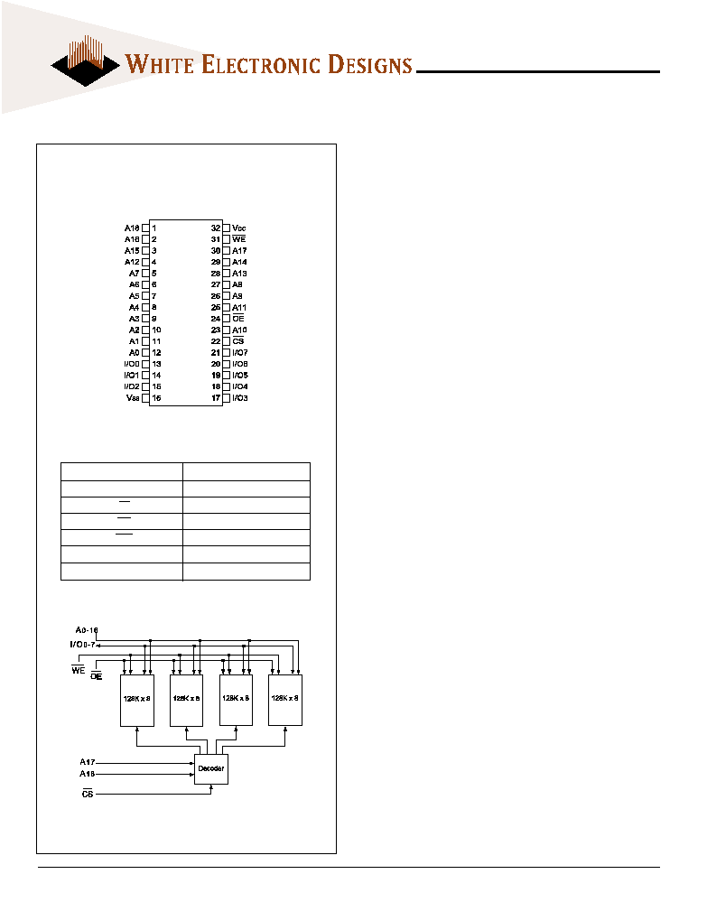
P
IN
C
ONFIGURATION
T
OP
V
IEW
F
IG
. 1
B
LOCK
D
IAGRAM
A0-18
Address Inputs
I/O0- 7
Data Input/Output
CS
Chip Select
OE
Output Enable
WE
Write Enable
VCC
+5.0V Power
VSS
Ground
P
IN
D
ESCRIPTION
512Kx8 CMOS EEPROM, WE512K8-XCX, SMD 5962-93091
May 2000 Rev.1

2
White Electronic Designs Corporation Phoenix AZ (602) 437-1520
WE512K8, WE256K8,
WE128K8-XCX
256Kx8 CMOS EEPROM, WE256K8-XCX, SMD 5962-93155
F
IG
.2
P
IN
C
ONFIGURATION
T
OP
V
IEW
256KX8 BIT CMOS EEPROM
MODULE
FEATURES
Read Access Times of 150, 200ns
JEDEC Standard 32 Pin, Hermetic Ceramic DIP
(Package 302)
Commercial, Industrial and Military Temperature
Ranges
MIL-STD-883 Compliant Devices Available
Write Endurance 10,000 Cycles
Data Retention at 25∞C, 10 Years
Low Power CMOS Operation:
2mA Standby Typical/90mA Operating Maximum
Automatic Page Write Operation
Internal Address and Data Latches for
512 Bytes, 1 to 64 Bytes/Row, Eight Pages
Page Write Cycle Time 10mS Max.
Data Polling for End of Write Detection
Hardware and Software Data Protection
TTL Compatible Inputs and Outputs
B
LOCK
D
IAGRAM
P
IN
D
ESCRIPTION
A0-17
Address Inputs
I/O0-7
Data Input/Output
CS
Chip Select
OE
Output Enable
WE
Write Enable
VCC
+5.0V Power
VSS
Ground

3
White Electronic Designs Corporation (602) 437-1520 www.whiteedc.com
WE512K8, WE256K8,
WE128K8-XCX
128Kx8 CMOS EEPROM, WE128K8-XCX, SMD 5962-93154
128KX8 BIT CMOS EEPROM
MODULE
FEATURES
Read Access Times of 150, 200ns
JEDEC Standard 32 Pin, Hermetic Ceramic DIP
(Package 300)
Commercial, Industrial and Military Temperature
Ranges
MIL-STD-883 Compliant Devices Available
Write Endurance 10,000 Cycles
Data Retention at 25∞C, 10 Years
Low Power CMOS Operation:
1mA Standby Typical/70mA Operating
Automatic Page Write Operation
Internal Address and Data Latches for
256 Bytes, 1 to 64 Bytes/Row, Four Pages
Page Write Cycle Time 10mS Max.
Data Polling for End of Write Detection
Hardware and Software Data Protection
TTL Compatible Inputs and Outputs
F
IG
. 3
P
IN
C
ONFIGURATION
T
OP
V
IEW
P
IN
D
ESCRIPTION
A0-16
Address Inputs
I/O0-7
Data Input/Output
CS
Chip Select
OE
Output Enable
WE
Write Enable
VCC
+5.0V Power
VSS
Ground
B
LOCK
D
IAGRAM
4
White Electronic Designs Corporation Phoenix AZ (602) 437-1520
WE512K8, WE256K8,
WE128K8-XCX
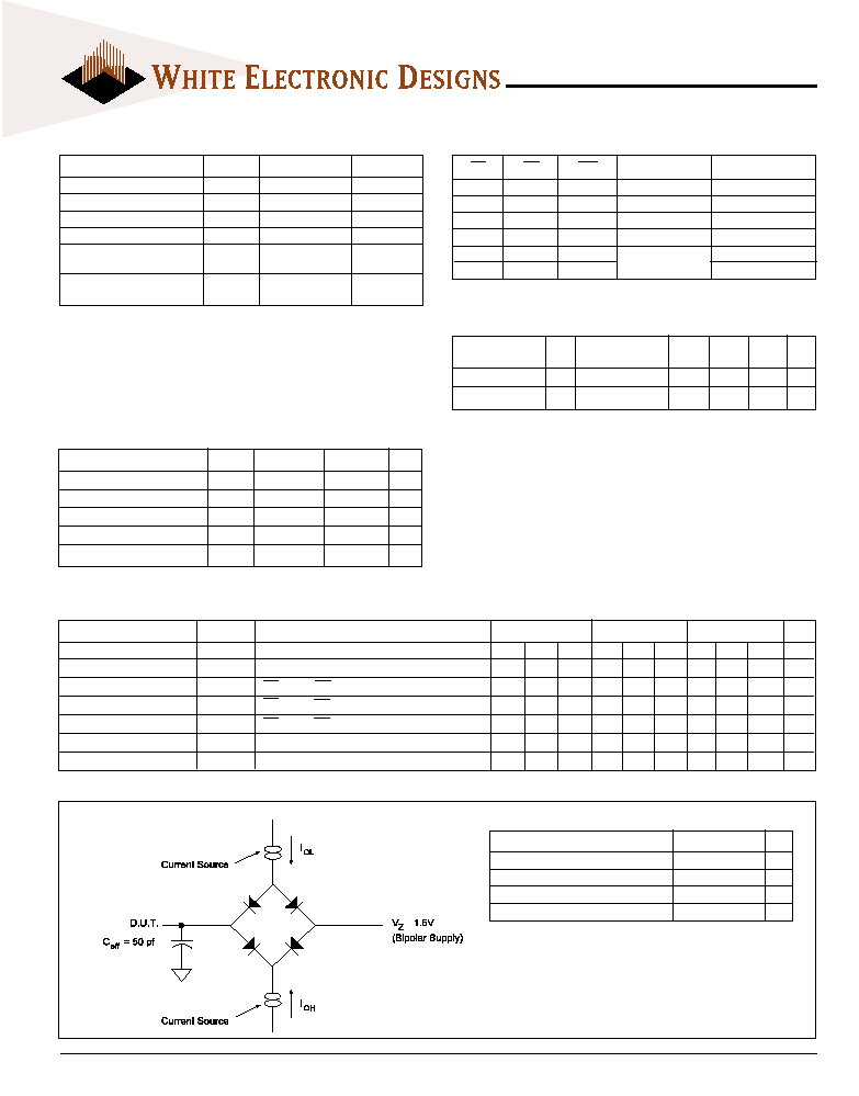
Parameter
Symbol
Conditions
512K x 8
256K x 8
128K x 8
Unit
Min Typ Max Min Typ Max Min Typ Max
Input Leakage Current
I
LI
V
CC
= 5.5, V
IN
= GND to V
CC
10
10
10
µA
Output Leakage Current
I
LO
CS = V
IH
, OE = V
IH
, V
OUT
= GND to V
CC
10
10
10
µA
Dynamic Supply Current
I
CC
CS = V
IL
, OE = V
IH
, f = 5MHz, V
CC
= 5.5
80
100
60
90
50
70
mA
Standby Current
I
SB
CS = V
IL
, OE = V
IH
, f = 5MHz, V
CC
= 5.5
3
8
2
6
1
4
mA
Output Low Voltage
V
OL
I
OL
= 2.1mA, V
CC
= 4.5V
0.45
0.45
0.45
V
Output High Voltage
V
OH
I
OH
= -400µA, V
CC
= 4.5V
2.4
2.4
2.4
V
NOTE: DC test conditions: V
IH
= V
CC
-0.3V, V
IL
= 0.3V
CS
OE
WE
Mode
Data I/O
H
X
X
Standby
High Z
L
L
H
Read
Data Out
L
H
L
Write
Data In
X
H
X
Out Disable
High Z/Data Out
X
X
H
Write
X
L
X
Inhibit
Parameter
Symbol
Unit
Operating Temperature
T
A
-55 to +125
∞C
Storage Temperature
T
STG
-65 to +150
∞C
Signal Voltage Any Pin
V
G
-0.6 to + 6.25 V
Voltage on OE and A9
-0.6 to +13.5 V
Thermal Resistance
q
JC
28
∞C/W
junction to case
Lead Temperature
+300
∞C
(soldering -10 secs)
T
RUTH
T
ABLE
A
BSOLUTE
M
AXIMUM
R
ATINGS
C
APACITANCE
(T
A
= +25∞C)
NOTE:
Stresses above those listed under "Absolute Maximum Ratings" may
cause permanent damage to the device. This is a stress rating only
and functional operation of the device at these or any other conditions
above those indicated in the operational sections of this specification
is not implied. Exposure to absolute maximum rating conditions for
extended periods may affect device reliability.
DC C
HARACTERISTICS
(V
CC
= 5.0V, V
SS
= 0V, T
A
= -55∞C
TO
+125∞C)
R
ECOMMENDED
O
PERATING
C
ONDITIONS
F
IG
. 4
AC T
EST
C
IRCUIT
AC T
EST
C
ONDITIONS
Notes:
V
Z
is programmable from -2V to +7V.
I
OL
& I
OH
programmable from 0 to 16mA.
Tester Impedance Z
0
= 75 ˝.
V
Z
is typically the midpoint of V
OH
and V
OL
.
I
OL
& I
OH
are adjusted to simulate a typical resistive load circuit.
ATE tester includes jig capacitance.
Parameter
Sym
Condition
512Kx8 256Kx8128Kx8 Unit
Max
Max
Max
Input Capacitance
C
IN
V
IN
= 0V, f = 1MHz
45
80
45
pF
Output Capacitance C
OUT
V
I/O
= 0V, f = 1MHz
60
80
60
pF
This parameter is guaranteed by design but not tested.
Parameter
Symbol
Min
Max
Unit
Supply Voltage
V
CC
4.55
.5
V
Input High Voltage
V
IH
2.0
V
CC
+ 0.3
V
Input Low Voltage
V
IL
-0.3
+0.8
V
Operating Temp. (Mil.)
T
A
-55
+125
∞C
Operating Temp. (Ind.)
T
A
-40
+85∞C
Parameter
Typ
Unit
Input Pulse Levels
V
IL
= 0, V
IH
= 3.0 V
Input Rise and Fall
5ns
Input and Output Reference Level
1.5V
Output Timing Reference Level
1.5V
5
White Electronic Designs Corporation (602) 437-1520 www.whiteedc.com
WE512K8, WE256K8,
WE128K8-XCX
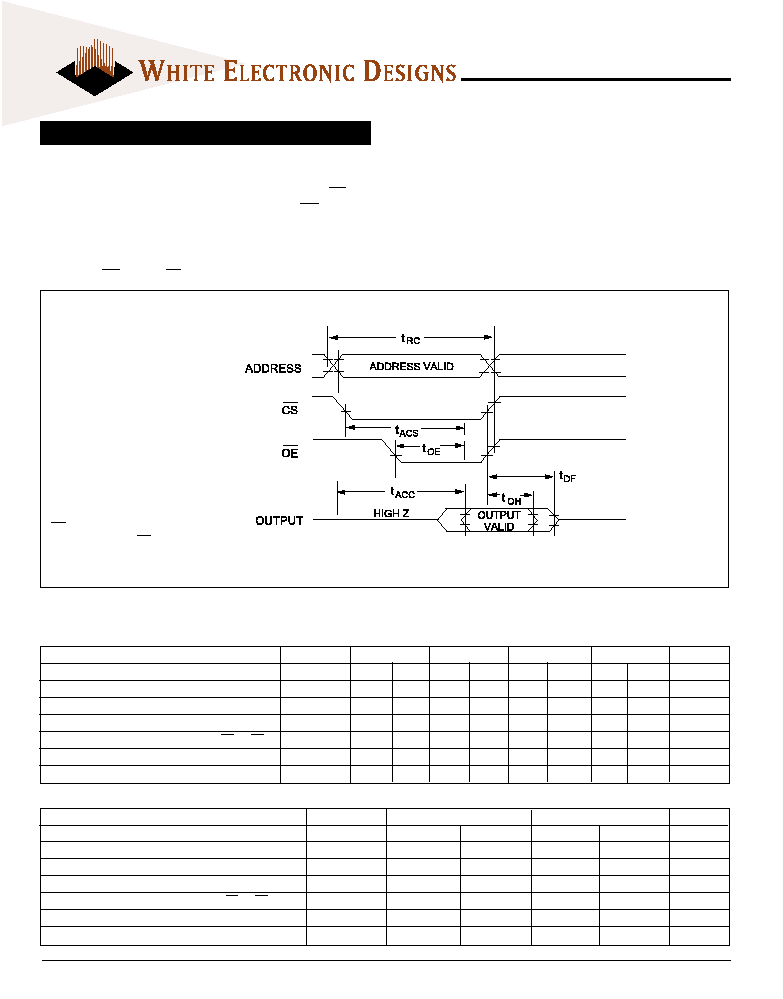
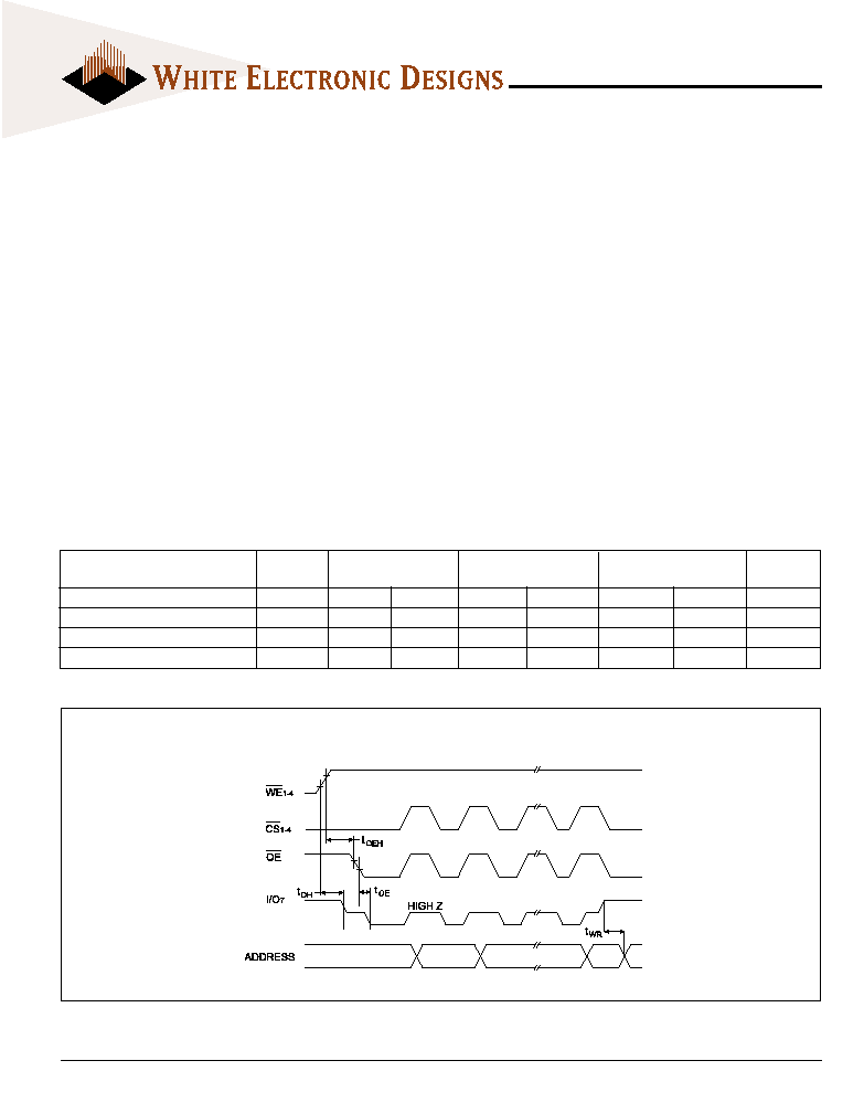
Figure 5 shows Read cycle waveforms. A read cycle be-
gins with selection address, chip select and output en-
able. Chip select is accomplished by placing the CS line
low. Output enable is done by placing the OE line low.
The memory places the selected data byte on I/O0
through I/O7 after the access time. The output of the
memory is placed in a high impedance state shortly after
either the OE line or CS line is returned to a high level.
AC READ CHARACTERISTICS (S
EE
F
IGURE
5)
FOR WE512K8-XCX
(V
CC
= 5.0V, V
SS
= 0V, T
A
= -55∞C
TO
+125∞C)
Parameter
Symbol
-150
-200
-250
-300
Unit
Min
Max
Min
Max
Min
Max
Min
Max
Read Cycle Time
t
RC
150
200
250
300
ns
Address Access Time
t
ACC
150
200
250
300
ns
Chip Select Access Time
t
ACS
150
200
250
300
ns
Output Hold from Address Change, OE or CS
t
OH
0
0
0
0
ns
Output Enable to Output Valid
t
OE
8585100
125
ns
Chip Select or Output Enable to High Z Output
t
DF
70
70
70
70
ns
FOR WE256K8-XCX
AND
WE128K8-XCX
Parameter
Symbol
-150
-200
Unit
Min
Max
Min
Max
Read Cycle Time
t
RC
150
200
ns
Address Access Time
t
ACC
150
200
ns
Chip Select Access Time
t
ACS
150
200
ns
Output Hold from Address Change, OE or CS
t
OH
10
10
ns
Output Enable to Output Valid
t
OE
85100
ns
Chip Select or Output Enable to High Z Output
t
DF
70
70
ns
F
IG
. 5
R
EAD
W
AVEFORMS
NOTE:
OE may be delayed up to t
ACS
-t
OE
after
the falling edge of CS without impact
on t
OE
or by t
ACC
-t
OE
after an address
change without impact on t
ACC
.
READ

6
White Electronic Designs Corporation Phoenix AZ (602) 437-1520
WE512K8, WE256K8,
WE128K8-XCX
NOTES:
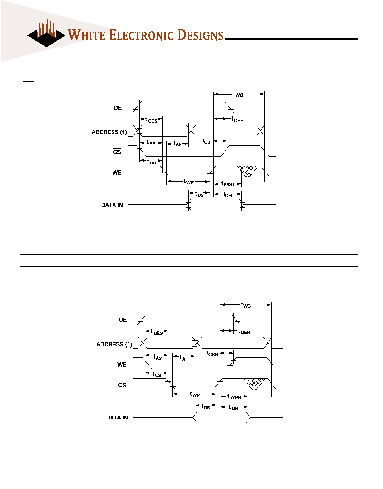
1. A
17
and A
18
must remain valid through WE and CS low pulse, for 512K x 8.
A
15
, A
16
, and A
17
must remain valid through WE and CS low pulse, for 256K x 8.
A
15
and A
16
must remain valid through WE and CS low pulse, for 128K x 8.
WRITE CYCLE TIMING
Figures 6 and 7 show the write cycle timing relation-
ships. A write cycle begins with address application,
write enable and chip select. Chip select is accom-
plished by placing the CS line low. Write enable con-
sists of setting the WE line low. The write cycle begins
when the last of either CS or WE goes low.
The WE line transition from high to low also initiates an
internal 150µsec delay timer to permit page mode op-
eration. Each subsequent WE transition from high to
low that occurs before the completion of the 150µsec
time out will restart the timer from zero. The operation
of the timer is the same as a retriggerable one-shot.
Write operations are initiated when both CS and WE
are low and OE is high. The EEPROM devices support
both a CS and WE controlled write cycle. The address
is latched by the falling edge of either CS or WE, which-
ever occurs last.
The data is latched internally by the rising edge of ei-
ther CS or WE, whichever occurs first. A byte write
operation will automatically continue to completion.
WRITE
AC WRITE CHARACTERISTICS
(V
CC
= 5.0V, V
SS
= 0V, T
A
= -55∞C
TO
+125∞C)
Parameter
Symbol 512K x 8
256K x 8
128K x 8
Unit
Min
Max
Min
Max
Min
Max
Write Cycle Time, TYP = 6mS
t
WC
10
10
10
ms
Address Set-up Time
t
AS
10
30
30
ns
Write Pulse Width (WE or CS)
t
WP
150
150
150
ns
Chip Select Set-up Time
t
CS
0
0
0
ns
Address Hold Time (1)
t
AH
125
50
50
ns
Data Hold Time
t
DH
10
0
0
ns
Chip Select Hold Time
t
CH
0
0
0
ns
Data Set-up Time
t
DS
100
100
100
ns
Output Enable Set-up Time
t
OES
10
30
30
ns
Output Enable Hold Time
t
OEH
10
0
0
ns
Write Pulse Width High
t
WPH
50
50
50
ns
7
White Electronic Designs Corporation (602) 437-1520 www.whiteedc.com
WE512K8, WE256K8,
WE128K8-XCX
F
IG
. 6
W
RITE
W
AVEFORMS
WE C
ONTROLLED
F
IG
. 7
W
RITE
W
AVEFORMS
CS C
ONTROLLED
NOTE:
1. Decoded Address Lines must be valid for the duration of the write.
NOTE:
1. Decoded Address Lines must be valid for the duration of the write.
8
White Electronic Designs Corporation Phoenix AZ (602) 437-1520
WE512K8, WE256K8,
WE128K8-XCX
DATA POLLING
Operation with data polling permits a faster method of
writing to the EEPROM. The actual time to complete
the memory programming cycle is faster than the guar-
anteed maximum.
The EEPROM features a method to determine when
the internal programming cycle is completed. After a
write cycle is initiated, the EEPROM will respond to read
cycles to provide the microprocessor with the status of
the programming cycle. The status consists of the last
data byte written being returned with data bit I/O
7
complemented during the programming cycle, and I/O
7
true after completion.
Data polling allows a simple bit test operation to deter-
mine the status of the EEPROM. During the internal
programming cycle, a read of the last byte written will
produce the complement of the data on I/O
7
. For ex-
ample, if the data written consisted of I/O
7
= HIGH, then
the data read back would consist of I/O
7
= LOW.
A polled byte write sequence would consist of the fol-
lowing steps:
1. write byte to EEPROM
2. store last byte and last address written
3. release a time slice to other tasks
4. read byte from EEPROM - last address
5. compare I/O
7
to stored value
a) If different, write cycle is not completed, go to
step 3.
b) If same, write cycle is completed, go to step 1
or step 3.
DATA POLLING AC CHARACTERISTICS
(V
CC
= 5.0V, V
CC
= 0V, T
A
= -55∞C
TO
+125∞C)
Parameter
Symbol
512Kx8
256Kx8
128Kx8
Unit
Min
Max
Min
Max
Min
Max
Data Hold Time
t
DH
10
0
0
ns
Output Enable Hold Time
t
OEH
10
0
0
ns
Output Enable To Output Delay
t
OE
100
100
100
ns
Write Recovery Time
t
WR
0
0
0
ns
F
IG
. 8
D
ATA
P
OLLING
W
AVEFORMS
9
White Electronic Designs Corporation (602) 437-1520 www.whiteedc.com
WE512K8, WE256K8,
WE128K8-XCX
Parameter
Symbol Min Max Unit
Write Cycle Time, TYP = 6mS
t
WC
10
ms
Data Set-up Time
t
DS
100
ns
Data Hold Time
t
DH
10
ns
Write Pulse Width
t
WP
150
ns
Byte Load Cycle Time
t
BLC
150
µs
Write Pulse Width High
t
WPH
5
0
ns
PAGE WRITE OPERATION
These devices have a page write operation that allows
one to 64 bytes of data (one to 128 bytes for the
WE512K8) to be written into the device and then simul-
taneously written during the internal programming pe-
riod. Successive bytes may be loaded in the same man-
ner after the first data byte has been loaded. An internal
timer begins a time out operation at each write cycle. If
another write cycle is completed within 150µs or less, a
new time out period begins. Each write cycle restarts
the delay period. The write cycles can be continued as
long as the interval is less than the time out period.
The usual procedure is to increment the least signifi-
cant address lines from A
0
through A
5
(A
0
through A
6
for
the WE512K8) at each write cycle. In this manner a page
of up to 64 bytes (128 bytes for the WE512K8) can be
loaded into the EEPROM in a burst mode before begin-
ning the relatively long interval programming cycle.
After the 150µs time out is completed, the EEPROM
begins an internal write cycle. During this cycle the en-
tire page of bytes will be written at the same time. The
internal programming cycle is the same regardless of
the number of bytes accessed.
PAGE
MODE CHARACTERISTICS
(V
CC
= 5.0V, V
SS
= 0V, T
A
= -55∞C
TO
+125∞C)
F
IG
. 9
P
AGE
W
RITE
W
AVEFORMS
Device
Block Address
Page Address
WE512K8-XCX
A
17
-A
18
A
7
-A
16
WE256K8-XCX
A
15
-A
17
A
6
-A
14
WE128K8-XCX
A
15
-A
16
A
6
-A
14
NOTE:
1. Decoded Address Lines must be valid for the duration of the write.
The page address must be the same for each byte load
and must be valid during each high to low transition of
WE (or CS). The block address also must be the same
for each byte load and must remain valid throughout
the WE (or CS) low pulse. The page and block address
lines are summarized below:

10
White Electronic Designs Corporation Phoenix AZ (602) 437-1520
WE512K8, WE256K8,
WE128K8-XCX
F
IG
. 10
S
OFTWARE
B
LOCK
D
ATA
P
ROTECTION
E
NABLE
A
LGORITHM
NOTES:
1. Data Format: I/O
7-0
(Hex);
Address Format: A
14
-A
0
(Hex).
A
17
and A
18
control selection of one of four blocks in the 512Kx8.
A
15
, A
16
, and A
17
control selection of one of 8 pages in the
256Kx8.
A
15
and A
16
control one of the four blocks in the 128Kx8.
2. Write Protect state will be activated at end of write even if no
other data is loaded.
3. Write Protect state will be deactivated at end of write period
even if no other data is loaded.
4. 1 to 128 bytes of data at each of 4 blocks may be loaded in the
512Kx8. 1 to 64 bytes of data at each of 8 blocks may be
loaded in the 256Kx8 and 1 to 64 bytes on 4 blocks in the
128Kx8.
(1)
LOAD DATA AA
TO
ADDRESS 5555
LOAD DATA 55
TO
ADDRESS 2AAA
LOAD DATA A0
TO
ADDRESS 5555
LOAD DATA XX
TO
ANY ADDRESS
(4)
LOAD LAST BYTE
TO
LAST ADDRESS
WRITES ENABLED
(2)
ENTER DATA
PROTECT STATE
11
White Electronic Designs Corporation (602) 437-1520 www.whiteedc.com
WE512K8, WE256K8,
WE128K8-XCX
HARDWARE DATA PROTECTION
Several methods of hardware data protection have been
implemented in the White Microelectronics EEPROM.
These are included to improve reliability during normal
operations.
a) V
CC
power on delay
As V
CC
climbs past 3.8V typical the device will wait
5mSec typical before allowing write cycles.
b) V
CC
sense
While below 3.8V typical write cycles are inhibited.
c) Write inhibiting
Holding OE low and either CS or WE high inhibits
write cycles.
d) Noise filter
Pulses of <8ns (typ) on WE or CS will not initiate a
write cycle.
(1)
F
IG
. 11
S
OFTWARE
B
LOCK
D
ATA
P
ROTECTION
D
ISABLE
A
LGORITHM
SOFTWARE DATA PROTECTION
A software write protection feature may be enabled or
disabled by the user. When shipped by White Micro-
electronics, the devices have the feature disabled. Write
access to the device is unrestricted.
To enable software write protection, the user writes three
access code bytes to three special internal locations.
Once write protection has been enabled, each write to
the EEPROM must use the same three byte write se-
quence to permit writing. After setting software data
protection, any attempt to write to the device without
the three-byte command sequence will start the inter-
nal write timers. No data will be written to the device,
however, for the duration of t
WC
. The write protection
feature can be disabled by a six byte write sequence of
specific data to specific locations. Power transitions
will not reset the software write protection.
Each 32K byte block (128K bytes for the WE512K8) of
EEPROM has independent write protection. One or
more blocks may be enabled and the rest disabled in
any combination. The software write protection guards
against inadvertent writes during power transitions or
unauthorized modification using a PROM programmer.
The block selection is controlled by the upper most ad-
dress lines (A
17
through A
18
for the WE512K8, A
15
through A
17
for the WE256K8, or A
15
and A
16
for the
WE128K8).
NOTES:
1. Data Format: I/O
7-0
(Hex);
Address Format: A
14
-A
0
(Hex).
A
17
and A
18
control selection of one of four blocks in the
512Kx8.
A
15
, A
16
, and A
17
control selection of one of 8 pages in the
256Kx8.
A
15
and A
16
control one of the four blocks in the 128Kx8.
2. Write Protect state will be activated at end of write even if no
other data is loaded.
3. Write Protect state will be deactivated at end of write period even
if no other data is loaded.
4. 1 to 128 bytes of data at each of 4 blocks may be loaded in the
512Kx8. 1 to 64 bytes of data at each of 8 blocks may be loaded
in the 256Kx8 and 1 to 64 bytes on 4 blocks in the 128Kx8.
EXIT DATA
PROTECT STATE
(3)
LOAD DATA AA
TO
ADDRESS 5555
LOAD DATA 55
TO
ADDRESS 2AAA
LOAD DATA 80
TO
ADDRESS 5555
LOAD DATA AA
TO
ADDRESS 5555
LOAD DATA 55
TO
ADDRESS 2AAA
LOAD DATA 20
TO
ADDRESS 5555
LOAD DATA XX
TO
ANY ADDRESS(4)
LOAD LAST BYTE
TO
LAST ADDRESS
12
White Electronic Designs Corporation Phoenix AZ (602) 437-1520
WE512K8, WE256K8,
WE128K8-XCX
P
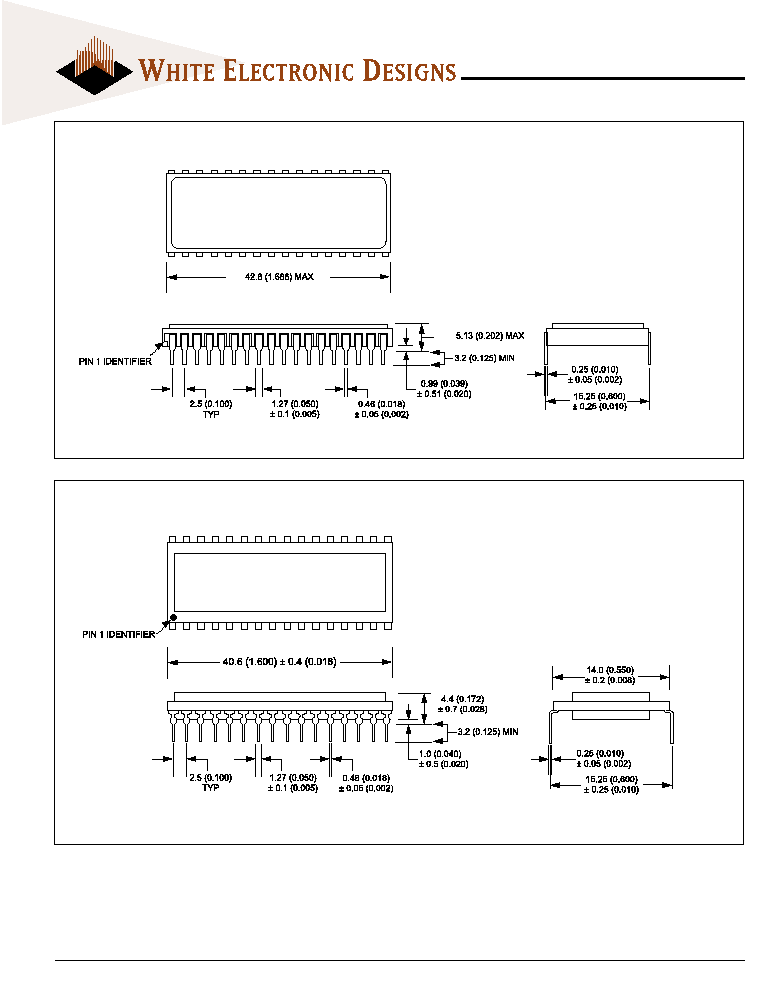
ACKAGE
300: 32 P
IN
, C
ERAMIC
D
IP
, S
INGLE
C
AVITY
S
IDE
B
RAZED
ALL LINEAR DIMENSIONS ARE MILLIMETERS AND PARENTHETICALLY IN INCHES
P
ACKAGE
302: 32 P
IN
, C
ERAMIC
D
IP
, D
UAL
C
AVITY
B
OTTOM
B
RAZED
ALL LINEAR DIMENSIONS ARE MILLIMETERS AND PARENTHETICALLY IN INCHES

13
White Electronic Designs Corporation (602) 437-1520 www.whiteedc.com
WE512K8, WE256K8,
WE128K8-XCX
O
RDERING
I
NFORMATION
LEAD FINISH:
Blank = Gold plated leads
A = Solder dip leads
PROCESSING:
Q = MIL-STD-883 Compliant
M = Military Screened
-55∞C to +125∞C
I = Industrial
-40∞C to +85∞C
C = Commercial
0∞C to +70∞C
PACKAGE:
C = Ceramic DIP (Package 300 for 128Kx8)
(Package 302 for 256Kx8)
(Package 300 for 512Kx8)
ACCESS TIME (ns)
ORGANIZATION, 512Kx8, 256Kx8 or 128Kx8
EEPROM
WHITE ELECTRONIC DESIGNS
512K x 8 EEPROM
150ns
32 pin DIP (C)
WE512K8-150CQ
5962-93091 01HYX
512K x 8 EEPROM
300ns
32 pin DIP (C)
WE512K8-300CQ
5962-93091 02HYX
512K x 8 EEPROM
250ns
32 pin DIP (C)
WE512K8-250CQ
5962-93091 03HYX
512K x 8 EEPROM
200ns
32 pin DIP (C)
WE512K8-200CQ
5962-93091 04HYX
256K x 8 EEPROM
200ns
32 pin DIP (C)
WE256K8-200CQ
5962-93155 01HYX
256K x 8 EEPROM
150ns
32 pin DIP (C)
WE256K8-150CQ
5962-93155 02HYX
128K x 8 EEPROM
200ns
32 pin DIP (C)
WE128K8-200CQ
5962-93154 01HXX
128K x 8 EEPROM
150ns
32 pin DIP (C)
WE128K8-150CQ
5962-93154 02HXX
W E XXXK8 - XXX C X X
DEVICE TYPE
SPEED
PACKAGE
WM PART NO.
SMD NO.
D
EVICE
T
YPE
S
PEED
P
ACKAGE
WM P
ART
N
O
.
SMD N
O
.