1
White Electronic Designs Corporation (602) 437-1520 www.whiteedc.com
WE32K32-XXX
White Electronic Designs
32Kx32 EEPROM MODULE, SMD 5962-94614
FEATURES
Access Times of 80*, 90, 120, 150ns
MIL-STD-883 Compliant Devices Available
Packaging:
68 lead, Hermetic CQFP (G2U), 122.4mm
(0.880") square, 3.56mm (0.140") height
(Package 510).
68 lead, Hermetic CQFP (G1U)
1
, 23.9mm
(0.940") square, 3.56mm (0.140") high (Pack
age 519)
68 lead, Hermetic CQFP (G1T), 23.9mm
(0.940") square, 4.06mm (0.160"), (Package
524)
66-pin, PGA Type, 1.075" square, Hermetic
Ceramic HIP (Package 400)
Data Retention at 25∞C, 10 Years
Write Endurance, 10,000 Cycles
Organized as 32Kx32; User Configurable 64Kx16
or 128Kx8
Commercial, Industrial and Military Temperature
Ranges
Automatic Page Write Operation
Page Write Cycle Time: 10ms Max
Data Polling for End of Write Detection
Hardware and Software Data Protection
TTL Compatible Inputs and Outputs
5 Volt Power Supply
Low Power CMOS, 10mA Standby Typical
Built-in Decoupling Caps and Multiple Ground
Pins for Low Noise Operation
* 80ns speed is not fully characterized and is subject to change or
cancellation without notice.
NOTE 1: Package not recommended for new design
P
IN
D
ESCRIPTION
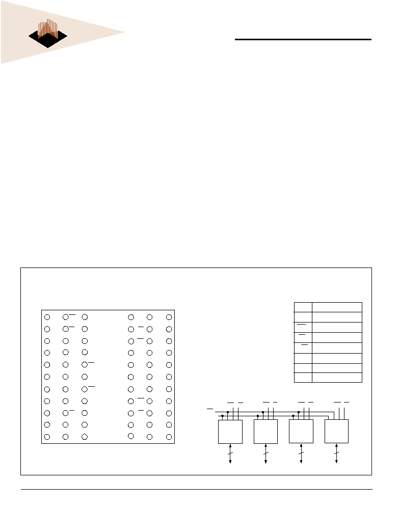
FIG. 1 PIN CONFIGURATION FOR WE32K32N-XH1X
TOP VIEW
I/O
0-31
Data Inputs/Outputs
A
0-14
Address Inputs
WE
1-4
Write Enables
CS
1-4
Chip Selects
OE
Output Enable
V
CC
Power Supply
GND
Ground
NC
Not Connected
B
LOCK
D
IAGRAM
October 2002 Rev. 3
32K x 8
8
I/O
0-7
WE CS
1
1
32K x 8
8
I/O
8-15
WE CS
2
2
32K x 8
8
I/O
16-23
WE CS
3
3
32K x 8
8
I/O
24-31
WE CS
4
4
A
0-14
OE
I/O
8
I/O
9
I/O
10
A
13
A
14
NC
NC
NC
I/O
0
I/O
1
I/O
2
WE
2
CS
2
GND
I/O
11
A
10
A
11
A
12
V
CC
CS
1
NC
I/O
3
I/O
15
I/O
14
I/O
13
I/O
12
OE
NC
WE
1
I/O
7
I/O
6
I/O
5
I/O
4
I/O
24
I/O
25
I/O
26
A
6
A
7
NC
A
8
A
9
I/O
16
I/O
17
I/O
18
V
CC
CS
4
WE
4
I/O
27
A
3
A
4
A
5
WE
3
CS
3
GND
I/O
19
I/O
31
I/O
30
I/O
29
I/O
28
A
0
A
1
A
2
I/O
23
I/O
22
I/O
21
I/O
20
11 22 33 44 55 66
1 12 23 34 45 56
2
White Electronic Designs Corporation Phoenix, AZ (602) 437-1520
White Electronic Designs
WE32K32-XXX
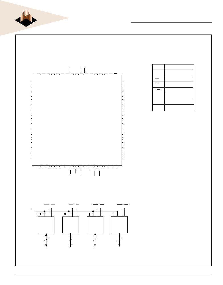
P
IN
D
ESCRIPTION
I/O
0-31
Data Inputs/Outputs
A
0-14
Address Inputs
WE
1-4
Write Enables
CS
1-4
Chip Selects
OE
Output Enable
V
CC
Power Supply
GND
Ground
NC
Not Connected
FIG. 2 PIN CONFIGURATION FOR WE32K32-XG2UX, WE32K32-XG1UX
1
,
AND WE32K32-XG1TX
B
LOCK
D
IAGRAM
T
OP
V
IEW
10
11
12
13
14
15
16
17
18
19
20
21
22
23
24
25
26
60
59
58
57
56
55
54
53
52
51
50
49
48
47
46
45
44
9 8 7 6 5 4 3 2 1 68 67 66 65 64 63 62 61
27 28 29 30 31 32 33 34 35 36 37 38 39 40 41 42 43
I/O
0
I/O
1
I/O
2
I/O
3
I/O
4
I/O
5
I/O
6
I/O
7
GND
I/O
8
I/O
9
I/O
10
I/O
11
I/O
12
I/O
13
I/O
14
I/O
15
V
CC
A
11
A
12
A
13
A
14
NC
NC
CS
1
OE
CS
2
NC
WE
2
WE
3
WE
4
NC
NC
NC
I/O
16
I/O
17
I/O
18
I/O
19
I/O
20
I/O
21
I/O
22
I/O
23
GND
I/O
24
I/O
25
I/O
26
I/O
27
I/O
28
I/O
29
I/O
30
I/O
31
NC
A
0
A
1
A
2
A
3
A
4
A
5
CS
3
GND
CS
4
WE
1
A
6
A
7
A
8
A
9
A
10
V
CC
32K x 8
8
I/O
0-7
WE CS
1
1
32K x 8
8
I/O
8-15
WE CS
2
2
32K x 8
8
I/O
16-23
WE CS
3
3
32K x 8
8
I/O
24-31
WE CS
4
4
A
0-14
OE
Note 1: Package not recommended for new design
3
White Electronic Designs Corporation Phoenix, AZ (602) 437-1520
White Electronic Designs
WE32K32-XXX
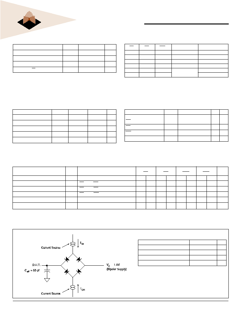
Parameter
Symbol
Conditions
-80
-90
-120
-150Units
Min
Max
Min Max
Min Max
Min
Max
Input Leakage Current
I
LI
V
CC
= 5.5, V
IN
= GND to V
CC
10
10
10
10
µA
Output Leakage Current
I
LO x 32
CS = V
IH
, OE = V
IH
, V
OUT
= GND to V
CC
10
10
10
10
µA
Operating Supply Current x 32 Mode I
CC x 32
CS = V
IL
, OE = V
IH
, f = 5MHz
320
250
200
150
mA
Standby Current
I
SB
CS = V
IH
, OE = V
IH
, f = 5MHz
2.5
2.5
2.5
2.5
mA
Output Low Voltage
V
OL
I
OL
= 2.1mA, V
CC
= 4.5V
0.45
0.45
0.45
0.45
V
Output High Voltage
V
OH
I
OH
= -400µA, V
CC
= 4.5V
2.4
2.4
2.4
2.4
V
NOTE: DC test conditions: V
IH
= V
CC
-0.3V, V
IL
= 0.3V
A
BSOLUTE
M
AXIMUM
R
ATINGS
DC C
HARACTERISTICS
(V
CC
= 5.0V, GND = 0V, T
A
= -55∞C
TO
+125∞C)
T
RUTH
T
ABLE
NOTE:
Stresses above those listed under "Absolute Maximum Ratings"
may cause permanent damage to the device. This is a stress
rating only and functional operation of the device at these or any
other conditions above those indicated in the operational sections
of this specification is not implied. Exposure to absolute maximum
rating conditions for extended periods may affect device reliability.
R
ECOMMENDED
O
PERATING
C
ONDITIONS
C
APACITANCE
(T
A
= 25∞ C)
F
IG
. 3 AC T
EST
C
IRCUIT
AC T
EST
C
ONDITIONS
Notes:
V
Z
is programmable from -2V to +7V.
I
OL
& I
OH
programmable from 0 to 16mA.
Tester Impedance Z
0
= 75 W.
V
Z
is typically the midpoint of V
OH
and V
OL
.
I
OL
& I
OH
are adjusted to simulate a typical resistive load circuit.
ATE tester includes jig capacitance.
CS
OE
WE
Mode
Data I/O
H
X
X
Standby
High Z
LL H
Read
Data Out
LH
L
Write
Data In
X
H
X
Out Disable
High Z/Data Out
X
X
H
Write
X
LX
Inhibit
Parameter
Symbol
Unit
Operating Temperature
T
A
-55 to +125
∞C
Storage Temperature
T
STG
-65 to +150
∞C
Signal Voltage Relative to GND
V
G
-0.6 to +6.25
V
Voltage on OE and A9
-0.6 to +13.5
V
Parameter
Symbol
Min
Max
Unit
Supply Voltage
V
CC
4.5
5.5
V
Input High Voltage
V
IH
2.0
V
CC
+ 0.3
V
Input Low Voltage
V
IL
-0.5
+0.8
V
Operating Temp. (Mil.)
T
A
-55
+125
∞C
Operating Temp. (Ind.)
T
A
-40
+85
∞C
Parameter
Symbol
Condition
Max Unit
Address Input Capacitance
C
AD
V
IN
= 0V, f = 1.0MHz 50
pF
OE Capacitance
C
OE
CS
1-4
Capacitance
C
CS
V
IN
= 0V, f = 1.0MHz 20
pF
WE
1-4
Capacitance
C
WE
V
IN
= 0V, f = 1.0MHz 20
pF
Data I/O Capacitance
C
I/O
V
IN
= 0V, f = 1.0MHz 20
pF
This parameter is guaranteed by design but not tested.
Parameter
Typ
Unit
Input Pulse Levels
V
IL
= 0, V
IH
= 3.0
V
Input Rise and Fall
5
ns
Input and Output Reference Level
1.5
V
Output Timing Reference Level
1.5
V
4
White Electronic Designs Corporation Phoenix, AZ (602) 437-1520
White Electronic Designs
WE32K32-XXX
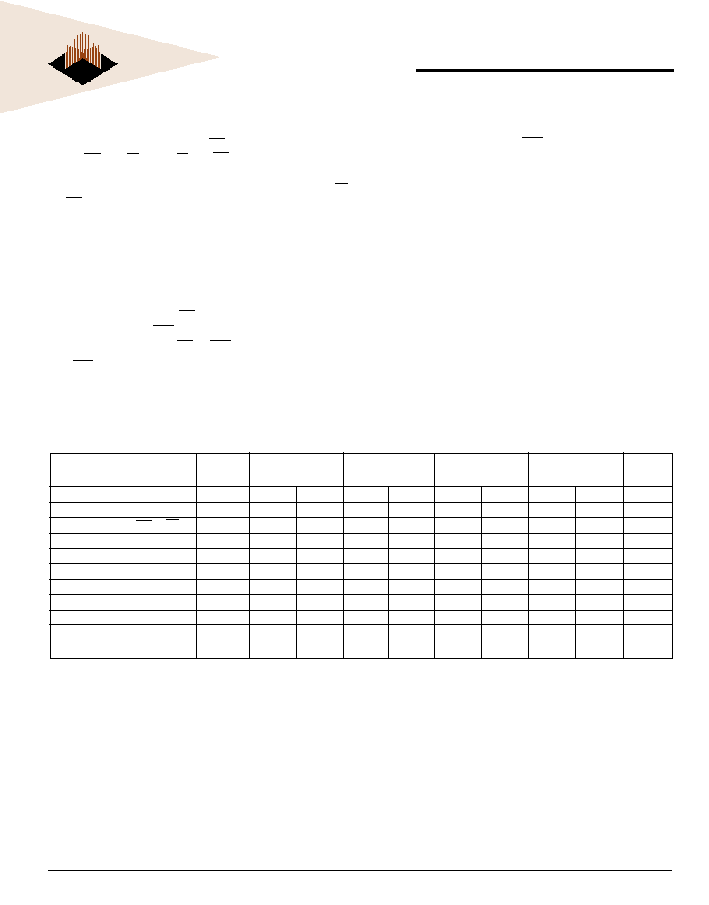
WRITE
AC W
RITE
C
HARACTERISTICS
(V
CC
= 5.0V, GND = 0V, T
A
= -55∞C
TO
+125∞C)
WRITE CYCLE
-80-90-120-150
Write Cycle Parameter
Symbol
Min
Max
Min
Max
Min
Max
Min
Max
Unit
Write Cycle Time, TYP = 6ms
t
WC
10
10
10
10
ms
Address Set-up Time
t
AS
0
0
30
30
ns
Write Pulse Width (WE or CS)
t
WP
100
100
150
150
ns
Chip Select Set-up Time
t
CS
0
0
0
0
ns
Address Hold Time
t
AH
50
50
100
100
ns
Data Hold Time
t
DH
0
0
10
10
ns
Chip Select Hold Time
t
CSH
0
0
0
0
ns
Data Set-up Time
t
DS
50
50
100
100
ns
Write Pulse Width High
t
WPH
50
50
50
50
ns
Output Enable Set-up Time
t
OES
10
10
10
10
ns
Output Enable Hold Time
t
OEH
10
10
10
10
ns
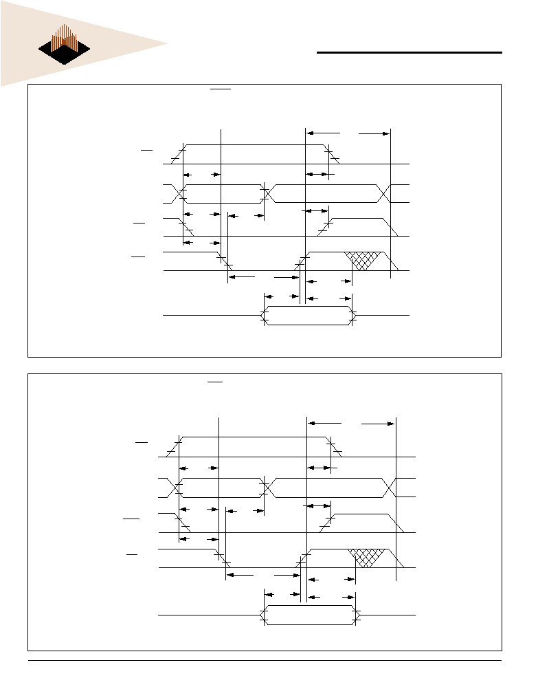
A write cycle is initiated when OE is high and a low pulse
is on WE or CS with CS or WE low. The address is
latched on the falling edge of CS or WE whichever oc-
curs last. The data is latched by the rising edge of CS
or WE, whichever occurs first. A byte write operation
will automatically continue to completion.
WRITE CYCLE TIMING
Figures 4 and 5 show the write cycle timing relation-
ships. A write cycle begins with address application,
write enable and chip select. Chip select is accom-
plished by placing the CS line low. Write enable con-
sists of setting the WE line low. The write cycle begins
when the last of either CS or WE goes low.
The WE line transition from high to low also initiates an
internal 150 µsec delay timer to permit page mode op-
eration. Each subsequent WE transition from high to
low that occurs before the completion of the 150 µsec
time out will restart the timer from zero. The operation
of the timer is the same as a retriggerable one-shot.
5
White Electronic Designs Corporation Phoenix, AZ (602) 437-1520
White Electronic Designs
WE32K32-XXX
FIG. 4 WRITE WAVEFORMS WE CONTROLLED
FIG. 5 WRITE WAVEFORMS CS CONTROLLED
t
ADDRESS
CS
1-4
WE
1-4
DATA IN
DH
t
WPH
t
WP
t
CSH
t
OEH
t
AH
t
OES
t
AS
t
CS
OE
t
WC
t
DS
t
ADDRESS
WE
1 - 4
CS
1 - 4
DATA IN
DH
t
WPH
t
WP
t
CSH
t
OEH
t
AH
t
OES
t
AS
t
CS
OE
t
DS
t
WC