1
White Electronic Designs Corporation ∑ (602) 437-1520 ∑ www.wedc.com
White Electronic Designs
WE512K16-XG4X
April 1999
Rev. 2
White Electronic Designs Corp. reserves the right to change products or specifi cations without notice.
512Kx16 CMOS EEPROM MODULE
FEATURES
Access Time of 140, 150, 200ns
Packaging:
∑ 68 lead, 40mm Hermetic CQFP (Package 501)
Organized as 4 banks of 128Kx16
Write
Endurance
10,000
Cycles
Data
Retention
Ten
Years
Minimum
Military
Temperature
Range
Low Power CMOS
Automatic Page Write Operation
Page Write Cycle Time: 10ms Max
Data Polling for End of Write Detection
Hardware and Software Data Protection
TTL Compatible Inputs and Outputs
5 Volt Power Supply
8 Built-in Decoupling Caps and Multiple Ground Pins for Low
Noise Operation
Weight - 20 grams typical
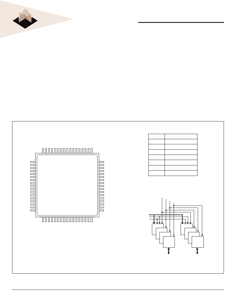
Block Diagram
128K x 8
I / O
0 - 7
CS
1
#
128K x 8
I / O
8 - 1 5
CS
3
#
C S
2
#
128K x 8
128K x 8
CS
4
#
A
0 - 1 6
O E #
W E #
128K x 8
128K x 8
128K x 8
128K x 8
NOTE: CS
1-4
# are used as bank selects. During reads, only one CSx#
can be active at one time.
FIGURE 1 ≠ PIN CONFIGURATION
Top View
10
11
12
13
14
15
16
17
18
19
20
21
22
23
24
25
26
60
59
58
57
56
55
54
53
52
51
50
49
48
47
46
45
44
9 8 7 6 5 4 3 2 1 68 67 66 65 64 63 62 61
27 28 29 30 31 32 33 34 35 36 37 38 39 40 41 42 43
I/O
0
I/O
1
I/O
2
I/O
3
I/O
4
I/O
5
I/O
6
I/O
7
GND
I/O
8
I/O
9
I/O
10
I/O
11
I/O
12
I/O
13
I/O
14
I/O
15
V
CC
A
11
A
12
A
13
A
14
A
15
A
16
CS
2
#
OE#
CS
4
#
NC
NC
NC
NC
NC
NC
NC
NC
NC
INC
NC
NC
NC
NC
NC
GND
NC
NC
NC
NC
NC
NC
NC
NC
NC
A
0
A
1
A
2
A
3
A
4
A
5
CS
1
#
GND
CS
3
#
WE#
A
6
A
7
A
8
A
9
A
10
V
CC
Pin Description
I/O0-15
Data Input/Output
A0-16
Address Inputs
WE#
Write Enable
CS1-4#
Chip Selects
OE#
Output Enable
V
CC
+5.0V Power
GND
Ground
NC
Not Connected
2
White Electronic Designs Corporation ∑ (602) 437-1520 ∑ www.wedc.com
White Electronic Designs
WE512K16-XG4X
April 1999
Rev. 2
White Electronic Designs Corp. reserves the right to change products or specifi cations without notice.
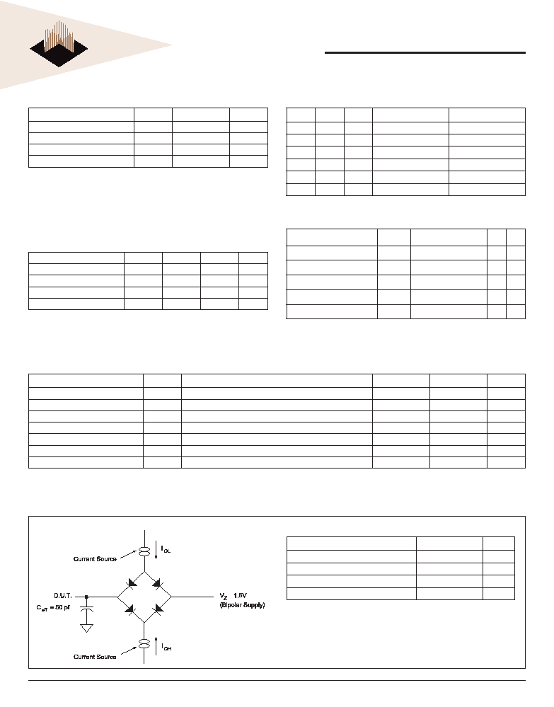
FIGURE 4
AC Test Circuit
DC CHARACTERISTICS
V
CC
= 5.0V, V
SS
= 0V, -55∞C T
A
+125∞C
Parameter
Symbol
Conditions
Min
Max
Unit
Input Leakage Current
I
LI
V
CC
= 5.5, V
IN
= GND to V
CC
10
µA
Output Leakage Current
I
LO
CS# = V
IH
, OE# = V
IH
, Vout = GND to V
CC
10
µA
Operating Supply Current (x16)
I
CCx16
CS1# = V
IL
, OE# = CS2-4# = V
IH
, f = 5MHz, V
CC
= 5.5
160
mA
Chip Erase Current
I
CC1
CS# = V
IL
, OE# = V
IH
, f = 5MHz, V
CC
= 5.5
250
mA
Standby Current
I
SB
CS# = V
IH
, OE# = V
IH
, f = 5MHz, V
CC
= 5.5
5
mA
Output Low Voltage
V
OL
I
OL
= 2.1mA, V
CC
= 4.5V
0.45
V
Output High Voltage
V
OH
I
OH
= -400µA, V
CC
= 4.5V
2.4
V
NOTE: DC test conditions: V
IH
= V
CC
-0.3V, V
IL
= 0.3V
TRUTH TABLE
CS#
OE#
WE#
Mode
Data I/O
H
X
X
Standby
High Z
L
L
H
Read
Data Out
L
H
L
Write
Data In
X
H
X
Out Disable
High Z/Data Out
X
X
H
Write
X
L
X
Inhibit
CAPACITANCE
T
A
= +25∞C
Parameter
Symbol
Conditions Max Unit
OE capacitance
COE
VIN = 0 V, f = 1.0 MHz
50
pF
WE capacitance
CWE
VIN = 0 V, f = 1.0 MHz
50
pF
CS1-4 capacitance
CCS
VIN = 0 V, f = 1.0 MHz
25
pF
Data I/O capacitance
CI/O
VI/O = 0 V, f = 1.0 MHz
40
pF
Address input capacitance
CAD
VIN = 0 V, f = 1.0 MHz
70
pF
This parameter is guaranteed by design but not tested.
ABSOLUTE MAXIMUM RATINGS
Parameter
Symbol
Unit
Operating Temperature
T
A
-55 to +125
∞C
Storage Temperature
T
STG
-65 to +150
∞C
Signal Voltage Relative to GND
V
G
-0.6 to + 6.25
V
Voltage on OE# and A9
-0.6 to +13.5
V
NOTE:
Stresses above those listed under "Absolute Maximum Ratings" may cause permanent
damage to the device. This is a stress rating only and functional operation of the device
at these or any other conditions above those indicated in the operational sections of
this specifi cation is not implied. Exposure to absolute maximum rating conditions for
extended periods may affect device reliability.
RECOMMENDED OPERATING CONDITIONS
Parameter
Symbol
Min
Max
Unit
Supply Voltage
V
CC
4.5
5.5
V
Input High Voltage
V
IH
2.0
V
CC
+ 0.3
V
Input Low Voltage
V
IL
-0.3
+0.8
V
Operating Temp. (Mil.)
T
A
-55
+125
∞C
AC TEST CONDITIONS
Parameter
Typ
Unit
Input Pulse Levels
V
IL
= 0, V
IH
= 3.0
V
Input Rise and Fall
5
ns
Input and Output Reference Level
1.5
V
Output Timing Reference Level
1.5
V
Notes: V
Z
is programmable from -2V to +7V.
I
OL
& I
OH
programmable from 0 to 16mA.
Tester Impedance Z0 = 75.
V
Z
is typically the midpoint of V
OH
and V
OL
.
I
OL
& I
OH
are adjusted to simulate a typical resistive load circuit.
ATE tester includes jig capacitance.
3
White Electronic Designs Corporation ∑ (602) 437-1520 ∑ www.wedc.com
White Electronic Designs
WE512K16-XG4X
April 1999
Rev. 2
White Electronic Designs Corp. reserves the right to change products or specifi cations without notice.
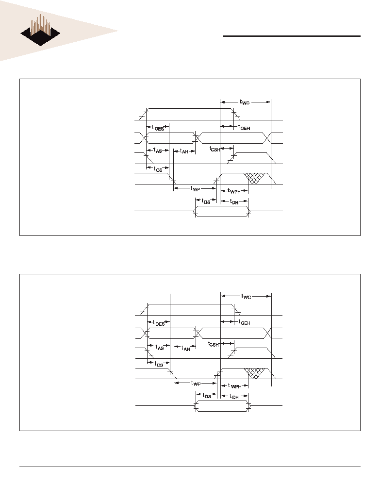
WRITE
A write cycle is initiated when OE# is high and a low pulse
is on WE# or CS# with CS# or WE# low. The address
is latched on the falling edge of CS# or WE# whichever
occurs last. The data is latched by the rising edge of CS#
or WE#, whichever occurs fi rst. A word write operation will
automatically continue to completion.
WRITE CYCLE TIMING
Figures 3 and 4 show the write cycle timing relationships.
A write cycle begins with address application, write enable
and chip select. Chip select is accomplished by placing
the CS# line low. Write enable consists of setting the WE#
line low. The write cycle begins when the last of either CS#
or WE# goes low.
The WE# line transition from high to low also initiates
an internal 150 µsec delay timer to permit page mode
operation. Each subsequent WE# transition from high to
low that occurs before the completion of the 150 µsec time
out will restart the timer from zero. The operation of the
timer is the same as a retriggerable one-shot.
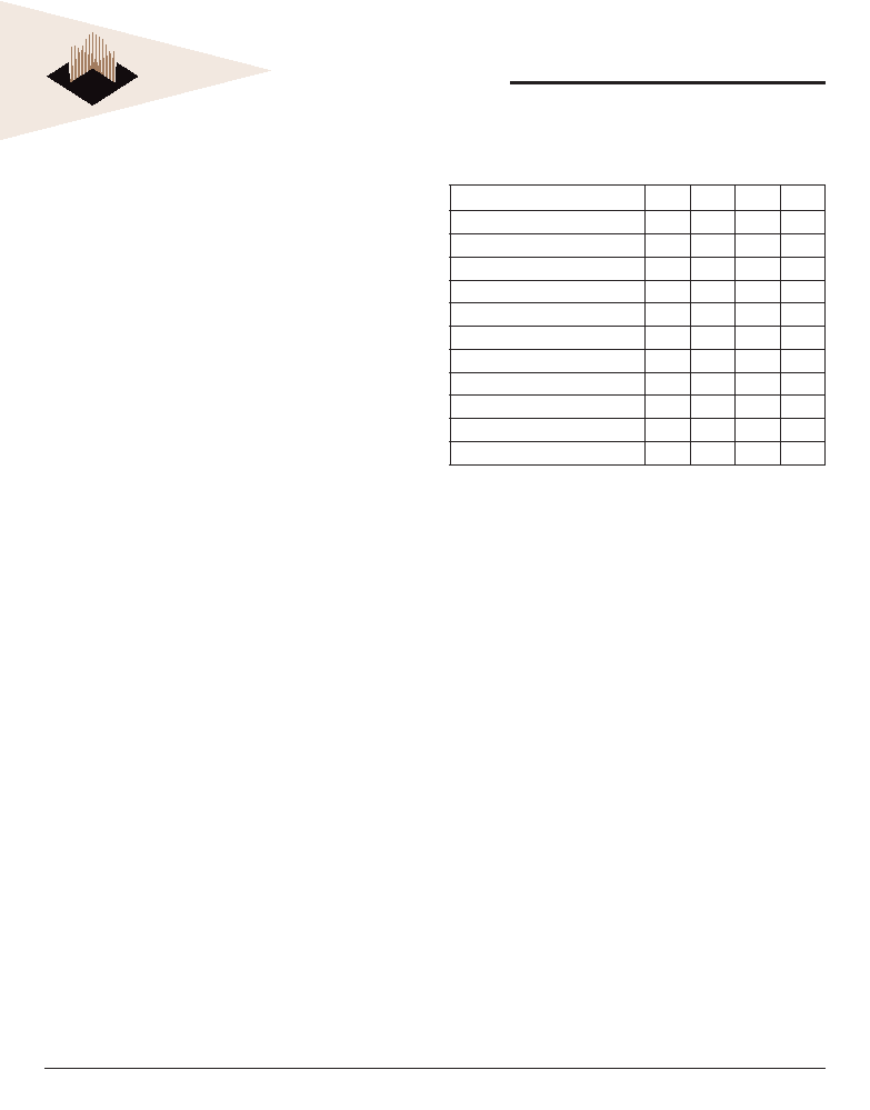
AC WRITE CHARACTERISTICS
V
CC
= 5.0V, V
SS
= 0V, -55∞C T
A
+125∞C
Write Cycle Parameter
Symbol
Min
Max
Unit
Write Cycle Time, TYP = 6ms
t
WC
10
ms
Address Set-up Time
t
AS
10
ns
Write Pulse Width (WE# or CS#)
t
WP
120
ns
Chip Select Set-up Time
t
CS
0
ns
Address Hold Time
t
AH
100
ns
Data Hold Time
t
DH
10
ns
Chip Select Hold Time
t
CSH
0
ns
Data Set-up Time
t
DS
100
ns
Output Enable Set-up Time
t
OES
10
ns
Output Enable Hold Time
t
OEH
10
ns
Write Pulse Width High
t
WPH
50
ns
4
White Electronic Designs Corporation ∑ (602) 437-1520 ∑ www.wedc.com
White Electronic Designs
WE512K16-XG4X
April 1999
Rev. 2
White Electronic Designs Corp. reserves the right to change products or specifi cations without notice.
OE#
ADDRESS
CS1-4#
WE#
DATA IN
OE#
ADDRESS
WE#
CS1-4#
DATA IN
FIGURE 3 ≠ WRITE WAVEFORM WE# CONTROLLED
FIGURE 4 ≠ WRITE WAVEFORM CS# CONTROLLED
5
White Electronic Designs Corporation ∑ (602) 437-1520 ∑ www.wedc.com
White Electronic Designs
WE512K16-XG4X
April 1999
Rev. 2
White Electronic Designs Corp. reserves the right to change products or specifi cations without notice.
ADDRESS
CS#
OE#
OUTPUT
READ
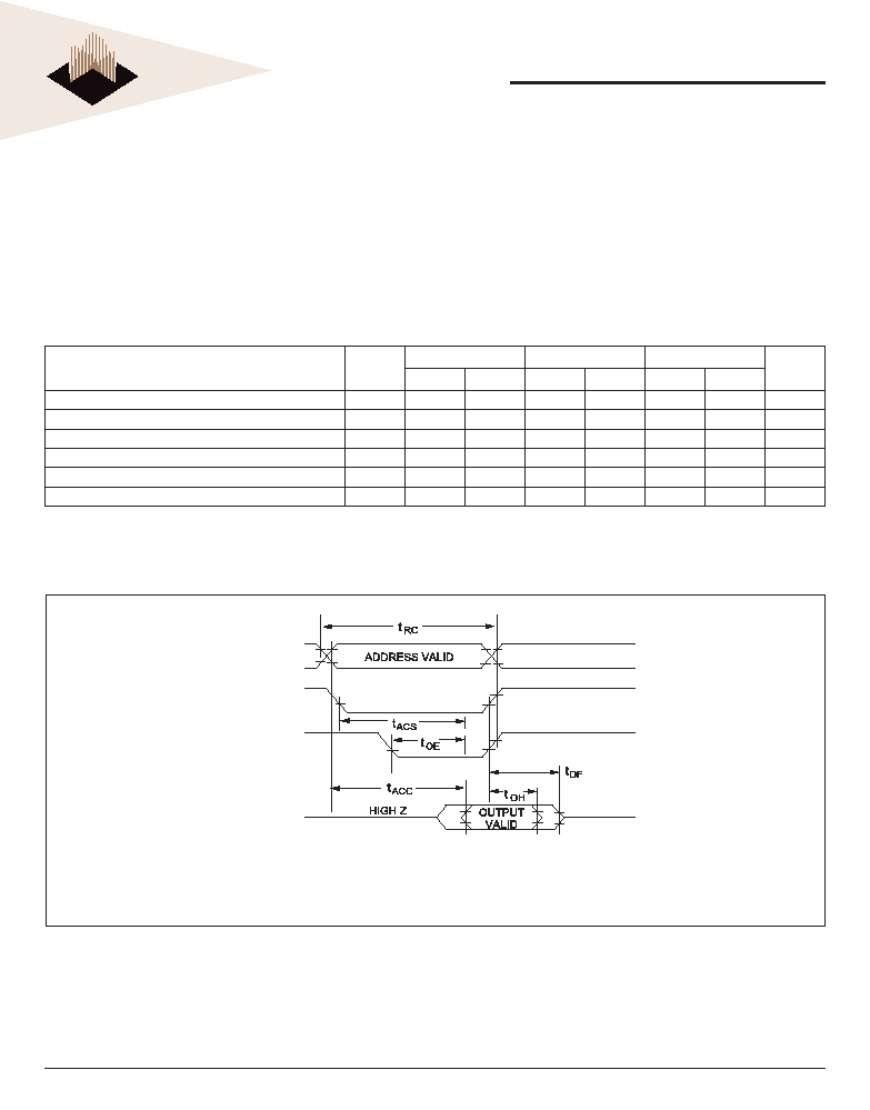
The module stores data at the memory location determined
by the address pins. When CS# and OE# are low and WE#
is high, this data is present on the outputs. When CS# and
OE# are high, the outputs are in a high impedance state.
This two line control prevents bus contention.
Notes:
OE# may be delayed up to t
ACS
- t
OE
after the falling edge of CS# without impact
on t
OE
or by t
ACC
- toe after an address change without impact on t
ACC
.
CS1-4# are used as bank selects.
During reads, only one CSx# can be active at one time.
AC READ CHARACTERISTICS
V
CC
= 5.0V, V
SS
= 0V, -55∞C T
A
+125∞C
Parameter
Symbol
-140
-150
-200
Unit
Min
Max
Min
Max
Min
Max
Read Cycle Time
trc
140
150
200
ns
Address Access Time
tacc
140
150
200
ns
Chip Select Access Time
tacs
140
150
200
ns
Output Hold from Address Change, OE# or CS#
toh
0
0
0
ns
Output Enable to Output Valid
toe
0
50
0
55
0
55
ns
Chip Select or OE# to High Z Output
tdf
50
70
70
ns
FIGURE 5 ≠ READ WAVEFORMS