1
White Electronic Designs Corporation ∑ (508) 366-5151 ∑ www.whiteedc.com
WED2CG472512V-D2
December 1999
ADVANCED*
DESCRIPTION
16MB (4x512Kx72) SYNC / SYNC BURST,
DUAL KEY DIMM SRAM MODULE
The WED2CG472512V is a Synchronous/Synchronous Burst SRAM,
84 position Dual Key; Double High DIMM (168 contacts) Module,
organized as 4x512Kx72. The Module contains sixteeen (16) Syn-
chronous Burst RAM devices, packaged in the industry standard
JEDEC 14mmx20mm TQFP placed on a Multilayer FR4 Substrate.
The Module Architecture is defined as a Sync/SyncBurst, Flow-
Through, with support for either linear or sequential burst. This
Module provides high performance, 2-1-1-1 accesses when used
in Burst Mode, and when used in Synchronous Only Mode, pro-
vides a high performance cost advantage over BiCMOS asynchro-
nous device architectures.
Synchronous Only operations are performed via strapping ADSC
Low, and ADSP/ADV High, which provides for Ultra Fast Accesses
in Read Mode while providing for internally self-timed Early
Writes.
Synchronous/Synchronous Burst operations are in relation to an
externally supplied clock, Registered Address, Registered Global
Write, Registered Enables as well as an Asynchronous Output
Enable. This Module has been defined with full flexibility, which
allows individual control of each of the eight bytes, as well as
Quad Words in both Read and Write Operations.
* This data sheet describes a product that may or may not be under development
and is subject to change or cancellation without notice.
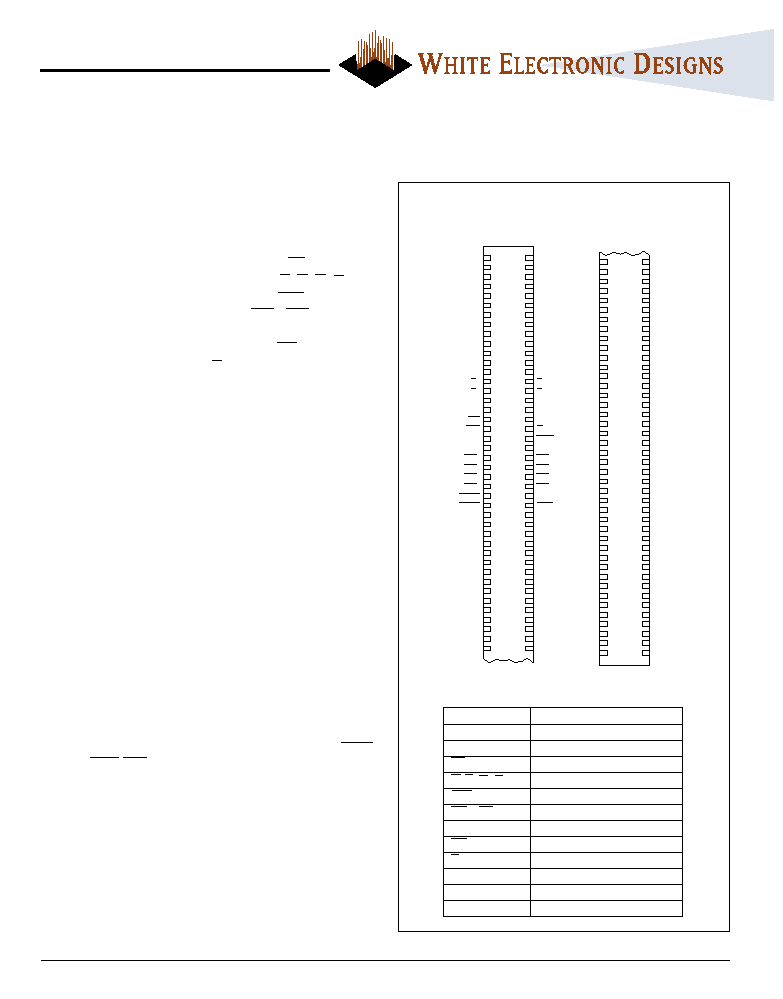
FIG. 1
PIN IDENTIFIER
PIN CONFIGURATION
V
SS
A
0
A
16
A
2
A
14
V
CC
A
4
A
12
A
6
A
10
V
SS
A
8
RFU
E
4
E
2
V
SS
MODE
EM
GW
RFU
V
CC
BW
4
BW
3
BW
8
BW
7
ADSC
ADSP
V
SS
NC
V
CC
DQ
0
DQ
1
DQ
2
DQ
3
V
SS
ZZ
1
V
CC
DQ
8
DQ
9
DQ
10
DQ
11
V
SS
V
SS
A
17
A
1
A
15
A
3
V
CC
A
13
A
5
A
11
A
7
V
SS
A
9
A
18
E
1
E
3
V
SS
CLK
V
SS
G
BWE
V
CC
BW
2
BW
1
BW
6
BW
5
V
SS
ADV
V
SS
DQP
0
V
CC
DQ
7
DQ
6
DQ
5
DQ
4
V
SS
DQP
1
V
CC
DQ
15
DQ
14
DQ
13
DQ
12
V
SS
1
2
3
4
5
6
7
8
9
10
11
12
13
14
15
16
17
18
19
20
21
22
23
24
25
26
27
28
29
30
31
32
33
34
35
36
37
38
39
40
41
42
85
86
87
88
89
90
91
92
93
94
95
96
97
98
99
100
101
102
103
104
105
106
107
108
109
110
111
112
113
114
115
116
117
118
119
120
121
122
123
124
125
126
43
44
45
46
47
48
49
50
51
52
53
54
55
56
57
58
59
60
61
62
63
64
65
66
67
68
69
70
71
72
73
74
75
76
77
78
79
80
81
82
83
84
127
128
129
130
131
132
133
134
135
136
137
138
139
140
141
142
143
144
145
146
147
148
149
150
151
152
153
154
155
156
157
158
159
160
161
162
163
164
165
166
167
168
NC
V
CC
DQ
16
DQ
17
DQ
18
DQ
19
V
SS
ZZ
2
V
CC
DQ
24
DQ
25
DQ
26
DQ
27
V
SS
NC
V
CC
DQ
32
DQ
33
DQ
34
DQ
35
V
SS
ZZ
3
V
CC
DQ
40
DQ
41
DQ
42
DQ
43
V
SS
NC
V
CC
DQ
48
DQ
49
DQ
50
DQ
51
V
SS
ZZ
4
V
CC
DQ
56
DQ
57
DQ
58
DQ
59
V
SS
DQP
2
V
CC
DQ
23
DQ
22
DQ
21
DQ
20
V
SS
DQP
3
V
CC
DQ
31
DQ
30
DQ
29
DQ
28
V
SS
DQP
4
V
CC
DQ
39
DQ
38
DQ
37
DQ
36
V
SS
DQP
5
V
CC
DQ
47
DQ
46
DQ
45
DQ
44
V
SS
DQP
6
V
CC
DQ
55
DQ
54
DQ
53
DQ
52
V
SS
DQP
7
V
CC
DQ
63
DQ
62
DQ
61
DQ
60
V
SS
FEATURES
s 4x512Kx72 Synchronous, Synchronous Burst
s Flow-Through Architecture
s Linear and Sequential Burst Support via MODE pin
s Clock Controlled Registered Module Enable (EM)
s Clock Controlled Registered Bank Enables (E
1
, E
2
, E
3
, E
4
)
s Clock Controlled Byte Write Mode Enable (BWE)
s Clock Controlled Byte Write Enables (BW
1
- BW
8
)
s Clock Controlled Registered Address
s Clock Controlled Registered Global Write (GW)
s Asynchronous Output Enable (G)
s Internally Self-Timed Write
s Individual Bank Sleep Mode Enables (ZZ
1
, ZZ
2
, ZZ
3
, ZZ
4
)
s Gold Lead Finish
s 3.3V
±
10% Operation
s Frequency(s): 100, 83, 67, 50MHz
s Access Speed(s): t
KHQV
= 9, 10, 12, 15ns
s Common Data I/O
s High Capacitance (30pF) Drive, at Rated Access Speed
s Single Total Array Clock
PIN DESCRIPTION
DQ
0
- DQ
63
Input/Output Bus
DQP
0
- DQP
7
Parity Bits
A
0
- A
18
Address Bus
EM
Module Enable
E
1
, E
2
, E
3
, E
4
Synchronous Bank Enables
BWE
Byte Write Mode Enable
BW
1
- BW
8
Byte Write Enables
CLK
Array Clock
GW
Synchronous Global Write Enable
G
Asynchronous Output Enable
ZZ
1
, ZZ
2
, ZZ
3
, ZZ
4
Bank Sleep Mode Enables
Vcc
3.3V Power Supply
Vss
Ground
2
White Electronic Designs Corporation ∑ (508) 366-5151 ∑ www.whiteedc.com
WED2CG472512V-D2
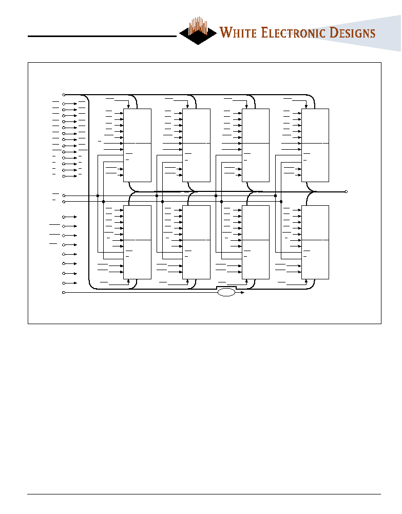
FIG. 2
FUNCTIONAL BLOCK DIAGRAM
ADDR
BW
8
BW
7
BW
6
BW
5
BW
4
BW
3
BW
2
BW
1
BWE
E
4
E
3
E
2
E
1
ADV
BW
4
BW
3
BW
2
BW
1
BWE
ADSP
ADSC
512K x 18
SBFT
512K x 18
SBFT
MODE
ADSP
ADSC
ADV
ZZ
1
ZZ
2
ZZ
3
ZZ
4
CLK
BW
8
BW
7
BW
6
BW
5
BW
4
BW
3
BW
2
BW
1
BWE
E
4
E
3
E
2
E
1
GW
G
E
1
ZZ
1
GW
G
BW
8
BW
7
BW
6
BW
5
BWE
ADSP
ADSC
ADV
512K x 18
SBFT
512K x 18
SBFT
E
1
ZZ
1
GW
G
ADV
BW
4
BW
3
BW
2
BW
1
BWE
ADSP
ADSC
512K x 18
SBFT
512K x 18
SBFT
E
2
ZZ
2
GW
G
BW
8
BW
7
BW
6
BW
5
BWE
ADSP
ADSC
ADV
512K x 18
SBFT
512K x 18
SBFT
E
2
ZZ
2
GW
G
ADV
BW
4
BW
3
BW
2
BW
1
BWE
ADSP
ADSC
512K x 18
SBFT
512K x 18
SBFT
E
3
ZZ
3
GW
G
BW
8
BW
7
BW
6
BW
5
BWE
ADSP
ADSC
ADV
512K x 18
SBFT
512K x 18
SBFT
E
3
ZZ
3
GW
G
ADV
BW
4
BW
3
BW
2
BW
1
BWE
ADSP
ADSC
512K x 18
SBFT
512K x 18
SBFT
E
4
ZZ
4
GW
G
BW
8
BW
7
BW
6
BW
5
BWE
ADSP
ADSC
ADV
512K x 18
SBFT
512K x 18
SBFT
E
4
ZZ
4
GW
G
U1 -U8 EQUAL LENGTH NET ROUTES
Data (DQ)
3
White Electronic Designs Corporation ∑ (508) 366-5151 ∑ www.whiteedc.com
WED2CG472512V-D2
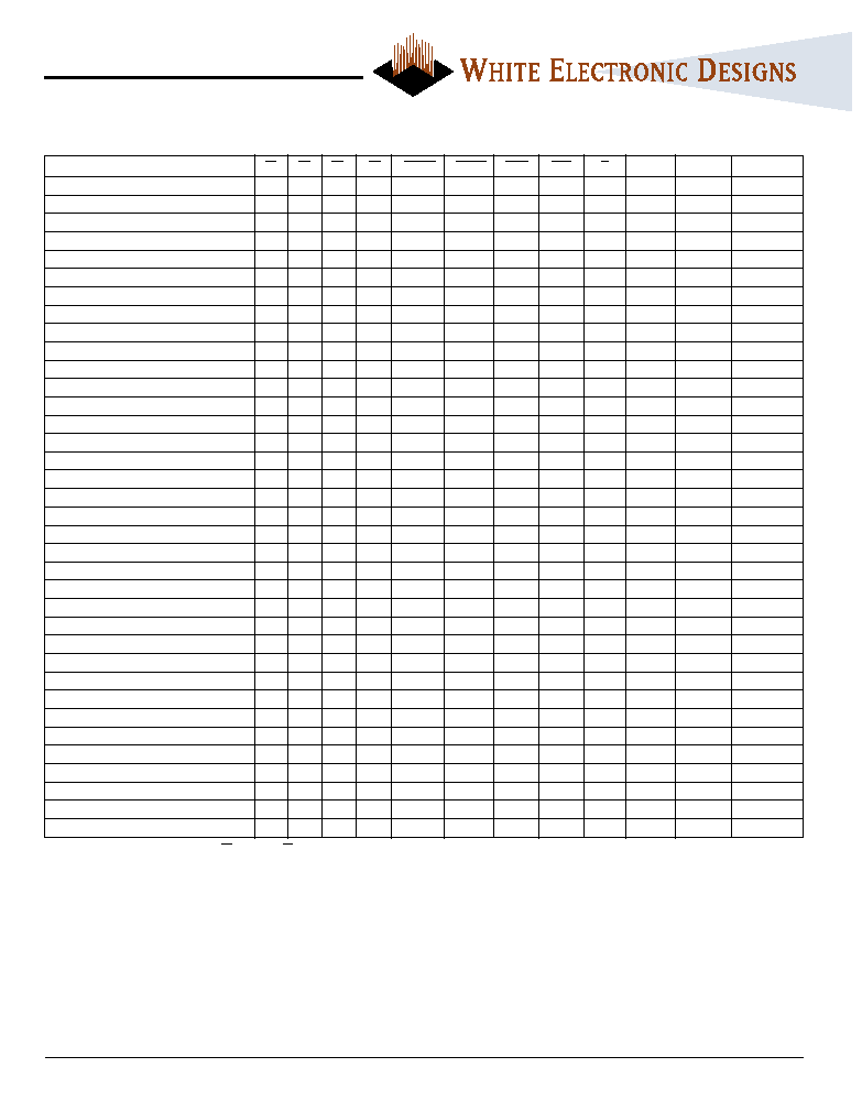
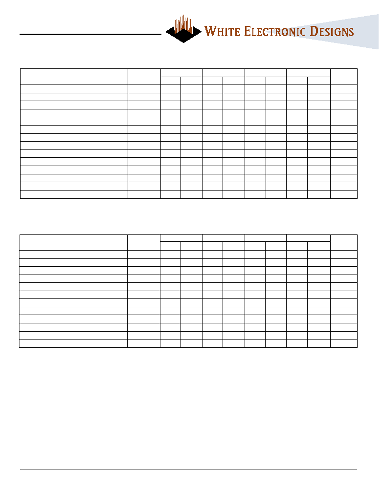
SYNC BURST ≠ TRUTH TABLE
Operation
E
1
E
2
E
3
E
4
ADSP
ADSC
ADV
GW
G
CLK
DQ
Addr. Used
Deselected Cycle, Power Down; Bank 1
H
X
*
*
X
L
X
X
X
L-H
High-Z
None
Deselected Cycle, Power Down; Bank 2
X
H
*
*
X
L
X
X
X
L-H
High-Z
None
Read Cycle, Begin Burst; Bank 1
L
H
*
*
L
X
X
X
L
L-H
Q
External
Read Cycle, Begin Burst; Bank 1
L
H
*
*
L
X
X
X
H
L-H
High-Z
External
Read Cycle, Begin Burst, Bank 2
H
L
*
*
L
X
X
X
L
L-H
Q
External
Read Cycle, Begin Burst; Bank 2
H
L
*
*
L
X
X
X
H
L-H
High-Z
External
Write Cycle, Begin Burst; Bank 1
L
H
*
*
H
L
X
L
X
L-H
D
External
Write Cycle, Begin Burst; Bank 2
H
L
*
*
H
L
X
L
X
L-H
D
External
Read Cycle, Begin Burst; Bank 1
L
H
*
*
H
L
X
H
L
L-H
Q
External
Read Cycle, Begin Burst; Bank 1
L
H
*
*
H
L
X
H
H
L-H
High-Z
External
Read Cycle, Begin Burst; Bank 2
H
L
*
*
H
L
X
H
L
L-H
Q
External
Read Cycle, Begin Burst; Bank 2
H
L
*
*
H
L
X
H
H
L-H
High-Z
External
Read Cycle, Continue Burst; Bank 1
X
H
*
*
X
H
L
H
L
L-H
Q
Next
Read Cycle, Continue Burst; Bank 1
X
H
*
*
X
H
L
H
H
L-H
High-Z
Next
Read Cycle, Continue Burst; Bank 2
H
X
*
*
X
H
L
H
L
L-H
Q
Next
Read Cycle, Continue Burst; Bank 2
H
X
*
*
X
H
L
H
H
L-H
High-Z
Next
Read Cycle, Continue Burst; Bank 1
H
H
*
*
X
H
L
H
L
L-H
Q
Next
Read Cycle, Continue Burst; Bank 1
H
H
*
*
X
H
L
H
H
L-H
High-Z
Next
Read Cycle, Continue Burst; Bank 2
H
H
*
*
X
H
L
H
L
L-H
Q
Next
Read Cycle, Continue Burst; Bank 2
H
H
*
*
X
H
L
H
H
L-H
High-Z
Next
Write Cycle, Continue Burst; Bank 1
X
H
*
*
H
H
L
L
X
L-H
D
Next
Write Cycle, Continue Burst; Bank 1
H
H
*
*
X
H
L
L
X
L-H
D
Next
Write Cycle, Continue Burst; Bank 2
H
X
*
*
H
H
L
L
X
L-H
D
Next
Write Cycle, Continue Burst; Bank 2
H
H
*
*
X
H
L
L
X
L-H
D
Next
Read Cycle, Suspend Burst; Bank 1
X
H
*
*
H
H
H
H
L
L-H
Q
Current
Read Cycle, Suspend Burst; Bank 1
X
H
*
*
H
H
H
H
H
L-H
High-Z
Current
Read Cycle, Suspend Burst; Bank 2
H
X
*
*
H
H
H
H
L
L-H
Q
Current
Read Cycle, Suspend Burst; Bank 2
H
X
*
*
H
H
H
H
H
L-H
High-Z
Current
Read Cycle, Suspend Burst; Bank 1
H
H
*
*
X
H
H
H
L
L-H
Q
Current
Read Cycle, Suspend Burst; Bank 1
H
H
*
*
X
H
H
H
H
L-H
High-Z
Current
Read Cycle, Suspend Burst; Bank 2
H
H
*
*
X
H
H
H
L
L-H
Q
Current
Read Cycle, Suspend Burst; Bank 2
H
H
*
*
X
H
H
H
H
L-H
High-Z
Current
Write Cycle, Suspend Burst; Bank 1
X
H
*
*
H
H
H
L
X
L-H
D
Current
Write Cycle, Suspend Burst; Bank 1
H
H
*
*
X
H
H
L
X
L-H
D
Current
Write Cycle, Suspend Burst; Bank 2
H
X
*
*
H
H
H
L
X
L-H
D
Current
Write Cycle, Suspend Burst; Bank 2
H
H
X
H
H
L
X
L-H
D
Current
* All truth Table Functions Repeat for Bank 3 (E
3
) and Bank 4 (E
4
).
4
White Electronic Designs Corporation ∑ (508) 366-5151 ∑ www.whiteedc.com
WED2CG472512V-D2
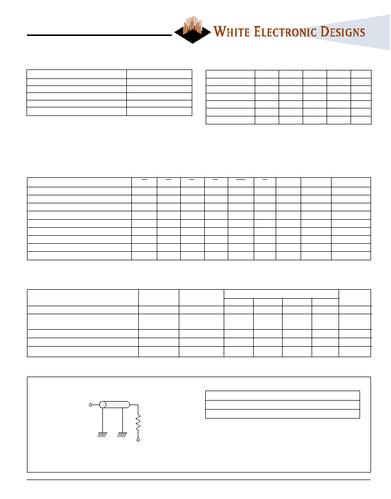
ABSOLUTE MAXIMUM RATINGS*
Voltage on V
cc
Relative to V
ss
-0.3V to +4.6V
V
in
-0.3V to V
cc
+0.5V
Storage Temperature
-55
∞
C to + 125
∞
C
Operating Temperature (Commercial)
0
∞
C to +70
∞
C
Operating Temperature (Industrial)
-40
∞
C to +85
∞
C
Short Circuit Output Current
100mA
*Stress greater than those listed under "Absolute Maximum Ratings" may cause permanent
damage to the device. This is a stress rating only and functional operation of the device
at these or any other conditions greater than those indicated in the operational sections of
this specification is not implied. Exposure to absolute maximum rating conditions for
extended periods may affect reliability.
RECOMMENDED DC OPERATING CONDITIONS
Parameter
Sym
Min
Typ
Max
Units
Supply Voltage
V
cc
3.3
3.3
3.6
V
Supply Voltage
V
ss
0
0
0
V
Input High
V
iH
2.0
3.0
V
cc
+0.3
V
Input Low
V
iL
-0.3
0
0.3
V
Input Leakage
I
Li
-2
1
2
µ
A
Output Leakage
I
Lo
-2
1
2
µ
A
AC TEST CONDITIONS
Input Pulse Levels
V
ss
to 3.0V
Input and Output Timing Ref.
1.25V
Output Test Equivalencies
see figure at left
DC ELECTRICAL CHARACTERISTICS READ CYCLE
Max
Description
Sym
Typ
8.5
10
12
15
Units
Power Supply Current
I
cc
1
2.0
2.9
2.7
2.7
2.5
A
Power Supply Current
I
cc
875
1.8
1.8
1.3
1.3
A
Device Selected, No Operation
Snooze Mode
I
cc
ZZ
270
350
350
350
350
mA
CMOS Standby
I
cc
3
500
700
700
700
700
mA
Clock Running-Deselect
I
cc
K
900
1.1
1.1
1.0
1.0
A
RL = 50
VL = 1.25V
DQ Output
Z0 = 50
Z0 = 50
AC TEST LOAD
Output Test Equivalencies
SYNCHRONOUS ONLY ≠ TRUTH TABLE
Operation
E
1
E
2
E
3
E
4
GW
G
ZZ
CLK
DQ
Synchronous Write - Bank 1
L
H
H
H
L
H
L
High-Z
Synchronous Read - Bank 1
L
H
H
H
H
L
L
Synchronous Write - Bank 2
H
L
H
H
L
H
L
High-Z
Synchronous Read - Bank 2
H
L
H
H
H
L
L
Synchronous Write - Bank 3
H
H
L
H
L
H
L
High-Z
Synchronous Read - Bank 3
H
H
L
H
H
L
L
Synchronous Write - Bank 4
H
H
H
L
L
H
L
High-Z
Synchronous Read - Bank 4
H
H
H
L
H
L
L
Snooze Mode
X
X
X
X
X
X
H
X
High-Z
5
White Electronic Designs Corporation ∑ (508) 366-5151 ∑ www.whiteedc.com
WED2CG472512V-D2
READ CYCLE TIMING PARAMETERS
9ns
10ns
12ns
15ns
Description
Sym
Min
Max
Min
Max
Min
Max
Min
Max
Units
Frequency
f
MAX
100
83
67
50
MHz
Clock Cycle Time
t
KHKH
10
12
15
20
ns
Clock High Time
t
KHKL
4
5
5
6
ns
Clock Low Time
t
KLKH
4
5
5
6
ns
Clock to Output Valid
t
KHQV
9
10
12
15
ns
Clock to Output Invalid
t
KHQX1
3
3
3
3
ns
Clock to Output Low-Z
t
KHQX
4
4
4
4
ns
Output Enable to Output Valid
t
GLQV
4
5
5
5
ns
Output Enable to Output Low-Z
t
GLQX
0
0
0
0
ns
Output Enable to Output High-Z
t
GHQZ
4
5
5
5
ns
Address Setup
t
AVKH
2.5
2.5
2.5
2.5
ns
Bank Enable Setup
t
EVKH
2.5
2.5
2.5
2.5
ns
Address Hold
t
KHAX
1.0
1.0
1.0
1.0
ns
Bank Enable Hold
t
KHEX
1.0
1.0
1.0
1.0
ns
WRITE CYCLE TIMING PARAMETERS
9ns
10ns
12ns
15ns
Description
Sym
Min
Max
Min
Max
Min
Max
Min
Max
Units
Frequency
f
MAX
100
83
67
50
MHz
Clock Cycle Time
t
KHKH
12
12
15
20
ns
Clock High Time
t
KHKL
4
5
5
6
ns
Clock Low Time
t
KLKH
4
5
5
6
ns
Address Setup
t
AVKH
2.5
2.5
2.5
2.5
ns
Address Hold
t
KHAX
1.0
1.0
1.0
1.0
ns
Bank Enable Setup
t
EVKH
2.5
2.5
2.5
2.5
ns
Bank Enable Hold
t
KHEX
1.0
1.0
1.0
1.0
ns
Global Write Enable Setup
t
WVKH
2.5
2.5
2.5
2.5
ns
Golbal Write Enable Hold
t
KHWX
1.0
1.0
1.0
1.0
ns
DataSetup
t
DVKH
2.5
2.5
2.5
2.5
ns
Data Hold
t
KHDX
1.0
1.0
1.0
1.0
ns