1
White Electronic Designs Corporation (508) 366-5151 www.whiteedc.com
White Electronic Designs
WED2DL36513V
July 2002 Rev. 3
ECO #14637
DESCRIPTION
The WEDC SyncBurst - SRAM family employs high-
speed, low-power CMOS designs that are fabricated
using an advanced CMOS process. WEDCs 16Mb
SyncBurst SRAMs integrate two 512K x 18 SRAMs into
a single BGA package to provide 512K x 36 configura-
tion. All synchronous inputs pass through registers con-
trolled by a positive-edge-triggered single-clock input
(CLK). The synchronous inputs include all addresses, all
data inputs, active LOW chip enable (CE), burst control
inputs (ADSC, ADSP, ADV), byte write enables (BW
0-3
)
and global write (GW). Asynchronous inputs include the
output enable (OE), clock (CLK) and snooze enable (ZZ).
There is also a burst mode input (MODE) that selects
between interleaved and linear burst modes. Write Cycles
can be from one to four bytes wide, as controlled by the
write control inputs. Burst operation can be initiated with
either address status processor (ADSP) or address sta-
tus controller (ADSC) inputs. Subsequent burst ad-
dresses can be internally generated as controlled by the
burst advance input (ADV).
* This data sheet describes a product under development, not fully
characterized, and is subject to change without notice.
512Kx36 Synchronous Pipeline Burst SRAM
FEATURES
Fast clock speed: 200, 166, 150 & 133MHz
Fast access times: 2.5ns, 3.5ns, 3.8ns & 4.0ns
Fast OE access times: 2.5ns, 3.5ns, 3.8ns 4.0ns
Available with 1.5ns setup and 0.5ns hold times or
1.0ns setup and hold times.
Single +3.3V power supply (V
DD
)
Seperate +3.3V or +2.5V isolated output buffer
supply (V
DDQ
)
Snooze Mode for reduced-power standby
Single-cycle deselect
Common data inputs and data outputs
Individual Byte Write control and Global Write
Clock-controlled and registered addresses, data
I/Os and control signals
Burst control (interleaved or linear burst)
Packaging:
119-bump BGA package
Low capacitive bus loading
IEEE 1149.1 JTAG Compatible Boundary Scan
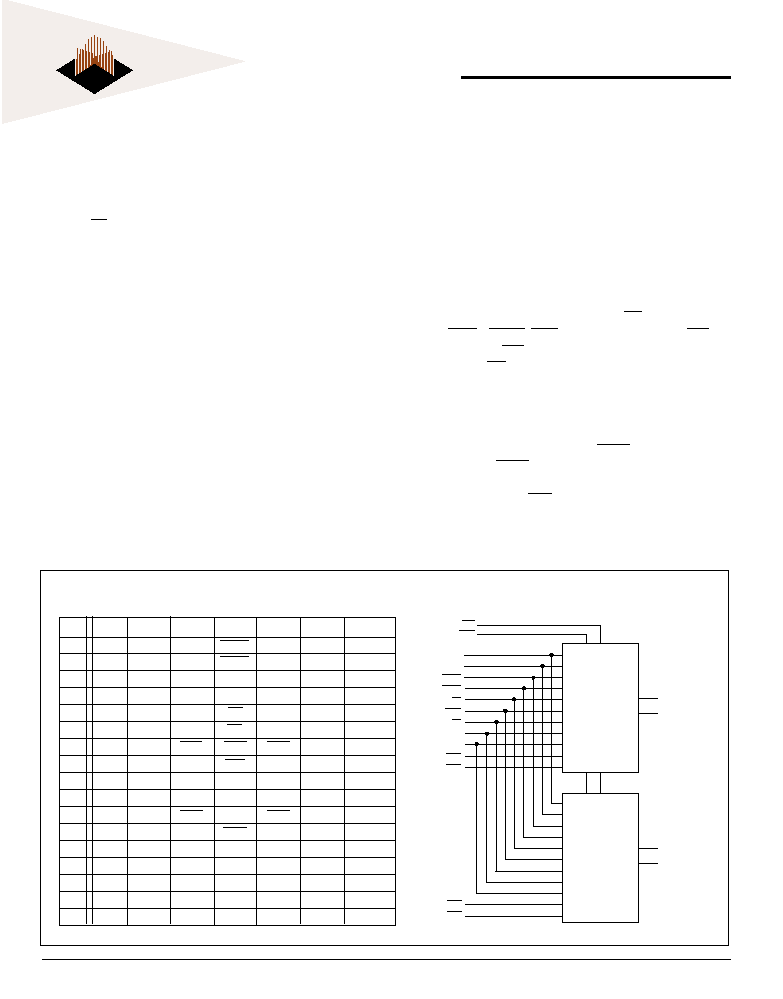
FIG. 1
B
LOCK
D
IAGRAM
P
IN
C
ONFIGURATION
(TOP VIEW)
1
2
3
4
5
6
7
A
V
DDQ
SA
SA
ADSP
SA
SA
V
DDQ
B
NC
SA
SA
ADSC
SA
SA
NC
C
NC
SA
SA
VDD
SA
SA
NC
D
DQc
DQPc
V
SS
NC
V
SS
DQPb
DQb
E
DQc
DQc
V
SS
CE
V
SS
DQb
DQb
F
V
DDQ
DQc
V
SS
OE
V
SS
DQb
V
DDQ
G
DQc
DQc
BWc
ADV
BWb
DQb
DQb
H
DQc
DQc
V
SS
GW
V
SS
DQb
DQb
J
V
DDQ
V
DD
NC
V
DD
NC
V
DD
V
DDQ
K
DQd
DQd
V
SS
CLK
V
SS
DQa
DQa
L
DQd
DQd
BWd
NC
BWa
DQa
DQa
M
V
DDQ
DQd
V
SS
BWE
V
SS
DQa
V
DDQ
N
DQd
DQd
V
SS
SA1
V
SS
DQa
DQa
P
DQd
DQPd
V
SS
SA0
V
SS
DQPa
DQa
R
NC
SA
MODE
V
DD
NC
SA
NC
T
NC
NC
SA
SA
SA
NC
ZZ
U
V
DDQ
TMD
TDI
TCK
TDO
NC
V
DDQ
DQ
b
,
DQP
b
DQ
a
,
DQP
a
GW
ADV
SA
CLK
ADSP
ADSC
OE
BWE
CE
MODE
ZZ
BW
a
BW
b
512K x 18
SSRAM
DQ
d
,
DQP
d
DQ
c
,
DQP
c
512K x 18
SSRAM
BW
c
BW
d
* Enable on pins C7 and R7 are options for the three CE density only.

2
White Electronic Designs Corporation Westborough MA (508) 366-5151
White Electronic Designs
WED2DL36513V
x36
Symbol Type
Description
CLK
Input
Pulse
The system clock input. All of the SSRAM inputs are sampled on the rising edge of the clock.
4P
SA0
Input
Synchronous Address Inputs: These inputs are registered and must meet the setup and hold
4N
SA1
times around the rising edge of CLK.
2A, 2C, 2R, 2B
SA
3A, 3B, 3C, 3T
4T, 5A, 5B, 5C,
5T, 6A, 6B, 6C, 6R
5L
BWa
Input
Synchronous Byte Write Enables: These active LOW inputs allow individual bytes to be written
5G
BWb
and must meet the setup and hold times around the rising edge of CLK. A byte write enable is
3G
BWc
LOW for a WRITE cycle and HIGH for a READ cycle.
3L
BWd
BWa controls DQas and DQPa; BWb controls DQbs and DQPb; BWc controls DQcs and DQPc;
BWd controls DQds and DQPd.
4M
BWE
Input
Byte Write Enable: This active LOW input permits BYTE WRITE operations and must meet the
setup and hold times around the rising edge of CLK.
4H
GW
Input
Global Write: This active LOW input allows a full 36- bit WRITE to occur independent of the BWE
and BWx lines and mustmeet the setup and hold times around the rising edge of CLK.
4K
CLK
Input
Clock: This signal registers the address, data, chip enable, byte write enables and burst control inputs
on its rising edge. All synchronous inputs must meet setup and hold times around the clocks rising edge.
4E
CE
Input
Synchronous Chip Enable: This active LOW input is used to enable the device and conditions the
internal use of ADSP. CE is sampled only when a new external address is loaded.
7TZZ
Input
Snooze Enable: T
his active HIGH, asynchronous input causes the device to enter a low-power standby
mode in which all data in the memory array is retained. When active, all other inputs are ignored.
4F
OE
Input
Output Enable: This active LOW, asynchronous input enables the data I/O output drivers.
4G
ADV
Input
Synchronous Address Advance: This active LOW input is used to advance the internal burst counter,
controlling burst access after the external address is loaded. A HIGH on ADV effectively causes wait
states to be generated (no address advance). To ensure use of correct address during a WRIT E
cycle, ADV must be HIGH at the rising edge of the first clock after an ADSP cycle is initiated.
4A
ADSP
Input
Synchronous Address Status Processor: This active LOW input interrupts any ongoing burst, causing
a new external address to be registered. A READ is performed using the new address, independent of
the byte write enables and ADSC, but dependent upon CE, CE
2
and CE
2
. ADSP is ignored if CE is
HIGH. Powerdown state is entered if CE
2
is LOW or CE
2
is HIGH.
4B
ADSC
Input
Synchronous Address Status Controller: This active LOW input interrupts any ongoing burst, causing
a new external address to be registered. A READ or WRITE is performed using the new address if CE
is LOW. ADSC is also used to place the chip into power-down state when CE is HIGH.
3R
MODE
Input
Mode: This input selects the burst sequence. A LOW on MODE selects linear burst. NC or HIGH on
this input selects interleaved burst. Do not alter input state while device is operating.
(a) 6K, 6L, 6M, 6N,
DQa
Input/
SRAM Data I/Os: Byte a is DQas; Byte b is DQbs; Byte c is DQcs;
7K, 7L, 7N, 7P
Output
Byte d is DQds. Input data must meet setup and hold times around rising edge of CLK.
(b) 6E, 6F, 6G, 6H,
DQb
7D, 7E, 7G, 7H
(c) 1D, 1E, 1G, 1H
DQc
2E, 2F, 2G, 2H
(d) 1K, 1L, 1N, 1P,
DQd
2K, 2L, 2M, 2N
6P
DQPa
Input/
Byte a Parity is DQPa; Byte b Parity is DQPb; Byte c Parity is DQPc;
6D
DQPb Output
Byte d Parity is DQPd.
2D
DQPc
2P
DQPd
2J, 4C, 4J, 4R, 6J
VDD
Supply
Power Supply: See DC Electrical Characteristics and Operating Conditions for range.
1A, 1F, 1J, 1M 1U
VDDQ Supply
Isolated Output Buffer Supply: See DC Electrical Characteristics and Operating
7A, 7F, 7J, 7M, 7U
Conditions for range.
3D, 3E, 3F, 3H, 3K,
VSS
Supply
Ground: GND.
3M, 3N, 3P, 5D, 5E,
5F, 5H, 5K, 5M, 5N,
5P
2U
TMS
Input
Scan Test Mode Select
3U
TDI
Input
Scan Test Data In
4U
TDO
Output
Scan Test Data Out
5U
TCK
Input
Scan Test Clock
P
IN
D
ESCRIPTION
3
White Electronic Designs Corporation (508) 366-5151 www.whiteedc.com
White Electronic Designs
WED2DL36513V
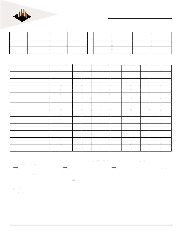
I
NTERLEAVED
B
URST
T
ABLE
(
MODE
=
NC
OR
HIGH
)
First Address Second Address Third Address Fourth Address
External
Internal
Internal
Internal
X...X00
X...X01
X...X10
X...X11
X...X01
X....X00
X...X11
X...X10
X...X10
X...X11
X...X00
X...X01
X...X11
X...X10
X...X01
X...X00
I
NTERLEAVED
B
URST
T
ABLE
(MODE = LOW)
First Address Second Address Third Address Fourth Address
External
Internal
Internal
Internal
X...X00
X...X01
X...X10
X...X11
X...X01
X....X10
X...X11
X...X00
X...X10
X...X11
X...X00
X...X01
X...X11
X...X00
X...X01
X...X10
T
RUTH
T
ABLE
Function
Address
CE
CE2
CE2
ZZ
ADSP
ADSC
ADV WRITE
OE
CLK
DQ
Used
Deselected Cycle, Power-Down
None
H
X
X
L
X
L
X
X
X
L-H
High-Z
Deselected Cycle, Power-Down
None
L
X
L
L
L
X
X
X
X
L-H
High-Z
Deselected Cycle, Power-Down
None
L
H
X
L
L
X
X
X
X
L-H
High-Z
Deselected Cycle, Power-Down
None
L
X
L
L
H
L
X
X
X
L-H
High-Z
Deselected Cycle, Power-Down
None
L
H
X
L
H
L
X
X
X
L-H
High-Z
SNOOZE MODE, Power-Down
None
X
X
X
H
X
X
X
X
X
X
High-Z
READ Cycle, Begin Burst
External
L
L
H
L
L
X
X
X
L
L-H
Q
READ Cycle, Begin Burst
External
L
L
H
L
L
X
X
X
H
L-H
High-Z
WRITE Cycle, Begin Burst
External
L
L
H
L
H
L
X
L
X
L-H
D
READ Cycle, Begin Burst
External
L
L
H
L
H
L
X
H
L
L-H
Q
READ Cycle, Begin Burst
External
L
L
H
L
H
L
X
H
H
L-H
High-Z
READ Cycle, Continue Burst
Next
X
X
X
L
H
H
L
H
L
L-H
Q
READ Cycle, Continue Burst
Next
X
X
X
L
H
H
L
H
H
L-H
High-Z
READ Cycle, Continue Burst
Next
H
X
X
L
X
H
L
H
L
L-H
Q
READ Cycle, Continue Burst
Next
H
X
X
L
X
H
L
H
H
L-H
High-Z
WRITE Cycle, Continue Burst
Next
X
X
X
L
H
H
L
L
X
L-H
D
WRITE Cycle, Continue Burst
Next
H
X
X
L
X
H
L
L
X
L-H
D
READ Cycle, Suspend Burst
Current
X
X
X
L
H
H
H
H
L
L-H
Q
READ Cycle, Suspend Burst
Current
X
X
X
L
H
H
H
H
H
L-H
High-Z
READ Cycle, Suspend Burst
Current
H
X
X
L
X
H
H
H
L
L-H
Q
READ Cycle, Suspend Burst
Current
H
X
X
L
X
H
H
H
H
L-H
High-Z
WRITE Cycle, Suspend Burst
Current
X
X
X
L
H
H
H
L
X
L-H
D
WRITE Cycle, Suspend Burst
Current
H
X
X
L
X
H
H
L
X
L-H
D
NOTES:
1. X means Dont Care.
means active LOW. H means logic HIGH. L means logic LOW.
2. For WRITE, L means any one or more byte write enable signals (BWa, BWb, BWc or BWd) and BWE are LOW or GW is LOW. WRITE = H for
all BWx, BWE, GW HIGH.
3. BWa enables WRITEs to DQas and DQPa. BWb enables WRITEs to DQbs and DQPb. BWc enables WRITEs to DQcs and DQPc. BWd
enables WRITEs to DQds and DQPd.
4. All inputs except OE and ZZ must meet setup and hold times around the rising edge (LOW to HIGH) of CLK.
5. Wait states are inserted by suspending burst.
6. For a WRITE operation following a READ operation, OE must be HIGH before the input data setup time and held HIGH throughout the input
data hold time.
7. This device contains circuitry that will ensure the outputs will be in High-Z during power-up.
8. ADSP LOW always initiates an internal READ at the L-H edge of CLK, a WRITE is performed by setting one or more byte write enable signals
and BWE LOW or GW LOW for the subsequent L-H edge of CLK. Refer to WRITE timing diagram for clarification.
4
White Electronic Designs Corporation Westborough MA (508) 366-5151
White Electronic Designs
WED2DL36513V
A
BSOLUTE
M
AXIMUM
R
ATINGS
*
Voltage on V
DD
Supply relative to V
SS
-0.5V to +4.6V
Voltage on V
DDQ
Supply relative to V
SS
-0.5V to +4.6V
V
IN
(DQx)
-0.5V to V
DDQ
+0.5V
V
IN
(Inputs)
-0.5V to V
DD
+0.5V
Storage Temperature (BGA)
+55�C to +125�C
Short Circuit Output Current
100 mA
*Stress greater than those listed under "Absolute Maximum Ratings"
may cause permanent damage to the device. This is a stress rating
only and functional operation of the device at these or any other
conditions greater than those indicated in the operational sections of
this specification is not implied. Exposure to absolute maximum rating
conditions for extended periods may affect reliability.
E
LECTRICAL
C
HARACTERISTICS
Description
Symbol
Conditions
Min
Max
Units
Notes
Input High (Logic 1)Voltage
V
IH
2.0
V
DD
+0.3
V
1
Input Low (Logic 0) Voltage
V
IL
-0.3
0.8
V
1
Input Leakage Current
I
LI
0V � V
IN
� V
DD
-1.0
1.0
�A
2
Ouptut Leakage Current
I
LO
Output(s) disabled, 0V � V
IN
� V
DD
-1.0
1.0
�A
Output High Voltage
V
OH
I
OH
= -4.0mA
2.4
V
1
Output Low Voltage
V
OL
I
OL
= 8.0mA
0.4
V
1
Supply Voltage
V
DD
3.135
3.6
V
1
Isolated Output Buffer Supply
V
DDQ
3.135
3.6
V
NOTES:
1. All voltages referenced to Vss (GND).
2. MODE has an internal pull-up, and input leakage is higher.
Description
Conditions
Symbol
Typ
Max
Units
Notes
Control Input Capacitance
T
A
= 25�C; f = 1MHz
C
I
3
4
pF
1
Input/Output Capacitance (DQ)
T
A
= 25�C; f = 1MHz
C
O
4
5
pF
1
Address Capacitance
T
A
= 25�C; f = 1MHz
C
A
3
5
pF
1
Clock Capacitance
T
A
= 25�C; f = 1MHz
C
CK
2.5
4
pF
1
NOTE:
1. This parameter is sampled.
B
GA
C
APACITANCE
P
ARITAL
T
RUTH
T
ABLE
- W
RITE
C
OMMANDS
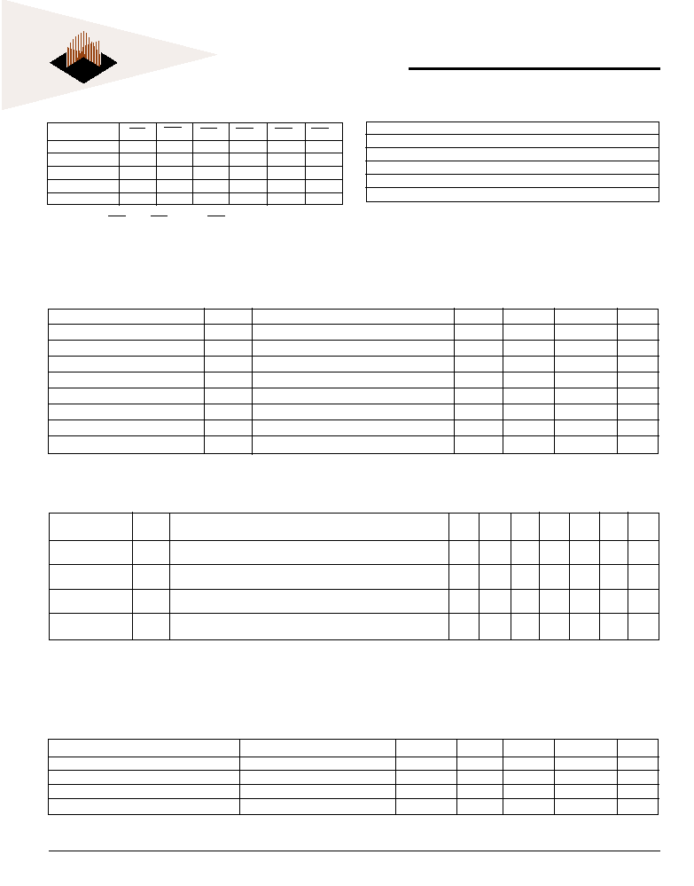
Function
GW
BWE
BWa
BWb
BWc
BWd
Read
H
H
X
X
X
X
Read
H
L
H
H
H
H
Write Byte a
H
L
L
H
H
H
Write All Bytes
H
L
L
L
L
L
Write All Bytes
L
X
X
X
X
X
NOTE: Using BWE and BWa through BWd, any one or more bytes
may be written.
Description
Symbol ConditionsTyp 200* 166
150
133 UnitsNotes
MHz MHz MHz MHz
Power Supply
Device selected; All inputs � V
IL
or V
IH
; Cycle time t
KC
MIN;
Current: Operating
I
DD
V
DD
= MAX; Outputs open
TBD
700
620
560
mA
1,2,3
Device deselected; V
DD
= MAX; All inputs � V
SS
+ 0.2
CMOS Standby
I
SB
2
or V
DD
- 0.2; All inputs static; CLK frequency = 0
10
20
20
20
20
mA
2,3
Device deselected; V
DD
= MAX; All inputs � V
IL
or V
IH
;
TTL Standby
I
SB
3
All inputs static; CLD frequency = 0
20
40
40
40
40
mA
2,3
Device deselected; V
DD
= MAX; All inputs � V
SS
+ 0.2
Clock Running
I
SB
4
or V
DD
-0.2; Cycle time t
KC
MIN
80
TBD
180
160
140
mA
2,3
* Advanced Information
NOTES:
1.I
DD
is specified with no output current and increases with faster cycle times. I
DD
increases with faster cycle times and greater output loading.
2.Device deselected means device is in power-down mode as defined in the truth table. Device selected means device is active (not in power-
down mode).
3.Typical values are measured at 3.3V, 25�C and 10ns cycle time.
DC C
HARACTERISTICS
5
White Electronic Designs Corporation (508) 366-5151 www.whiteedc.com
White Electronic Designs
WED2DL36513V
AC C
HARACTERISTICS
(WED2DL36513V)
Symbol 200MHz 166MHz 150MHz 133MHz
Parameter
Min
Max
Min
Max
Min
Max
Min
Max
Units
Clock
Clock Cycle Time
t
KC
5.0
6.0
6.6
7.5
ns
Clock Frequency
t
KF
200
166
150
133
MHz
Clock HIGH Time
t
KH
2.0
2.4
2.6
2.6
ns
Clock LOW Time
t
KL
2.0
2.4
2.6
2.6
ns
Output Times
Clock to output valid
t
KQ
2.5
3.5
3.8
4.0
ns
Clock to output invalid (2)
t
KQX
1.5
1.25
1.25
1.5
ns
Clock to output on Low-Z (2,3,4)
t
KQLZ
0
0
0
0
ns
Clock to output in High-Z (2,3,4)
t
KQHZ
3.0
3.5
3.8
4.0
ns
OE to output valid (5)
t
OEQ
2.5
3.5
3.8
4.0
ns
OE to output in Low-Z (2,3,4)
t
OELZ
0
0
0
0
ns
OE to output in High Z (2,3,4)
t
OEHZ
2.5
3.5
3.8
4.0
ns
Setup Times
Address (6,7)
t
AS
1.5
1.5
1.5
1.5
ns
Address status (ADSC, ADSP) (6,7)
t
ADSS
1.5
1.5
1.5
1.5
ns
Address advance (ADV) (6,7)
t
AAS
1.5
1.5
1.5
1.5
ns
Write signals (BWa-BWd, BWE, GW) (6,7)
t
WS
1.5
1.5
1.5
1.5
ns
Data-in (6,7)
t
DS
1.5
1.5
1.5
1.5
ns
Chip enables (CE, CE
2
, CE
2
) (6,7)
t
CES
1.5
1.5
1.5
1.5
ns
Hold Times
Address (6,7)
t
AH
0.5
0.5
0.5
0.5
ns
Address status (ADSC, ADSP) (6,7)
t
ADSH
0.5
0.5
0.5
0.5
ns
Address advance (ADV) (6,7)
t
AAH
0.5
0.5
0.5
0.5
ns
Write Signals (BWa-BWd, BWE, GW) (6,7)
t
WH
0.5
0.5
0.5
0.5
ns
Data-in (6,7)
t
DH
0.5
0.5
0.5
0.5
ns
Chip Enables (CE, CE
2
, CE
2
) (6,7)
t
CEH
0.5
0.5
0.5
0.5
ns
NOTES:
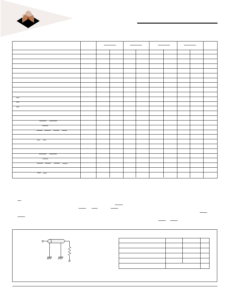
1. Test conditions as specified with the output loading as shown in Figure 1 for 3.3V I/0 and Figure 3 for 2.5V I/0 unless otherwise noted.
2. This parameter is measured with output load as shown in Figure 2 for 3.3V I/0 and Figure 4 for 2.5V I/0.
3. This parameter is sampled.
4. Transition is measured �500mV from steady state voltage.
5. OE is a Dont Care when a byte write enable is sampled LOW.
6. A WRITE cycle is defined by at least one byte write enable LOW and ADSP HIGH for the required setup and hold times. A READ cycle is
defined by all byte write enables HIGH and ADSC or ADV LOW or ADSP LOW for the required setup and hold times.
7. This is a synchronous device. All addresses must meet the specified setup and hold times for all rising edges of CLK when either ADSP or
ADSC is LOW and chip enabled. All other synchronous inputs must meet the setup and hold times with stable logic levels for all rising edges of
clock (CLK) when the chip is enabled. Chip enable must be valid at each rising edge of CLK when either ADSP or ADSC is LOW to remain enabled.
O
UTPUT
L
OADS
AC T
EST
C
ONDITIONS
50
Vt = 1.5V for 3.3V I/O
Vt = 1.25V for 2.5V I/O
Output
Z0 = 50
Z0 = 50
Parameter
3.3V I/O
2.5V I/O
Unit
Input Pulse Levels
V
SS
to 3.0 V
SS
to 2.5
V
Input Rise and Fall Times
1
1
ns
Input Timing Reference Levels
1.5
1.25
V
Output Timing Reference Levels
1.5
1.25
V
Output Load
See figure, at left
AC Output Load Equivalent

6
White Electronic Designs Corporation Westborough MA (508) 366-5151
White Electronic Designs
WED2DL36513V
SNOOZE MODE
SNOOZE MODE is a low-current, power-down mode
In which the device is deselected and current is reduced
to I
SB
2
Z
. The duration of SNOOZE MODE is dictated by
the length of time ZZ is in a HIGH state. After the device
enters SNOOZE MODE, all inputs except ZZ become
gated inputs and are ignored. ZZ is an asynchronous,
active HIGH input that causes the device to enter
Description
Conditions
Symbol
Min
Max
Units
Notes
Current during SNOOZE MODE
ZZ � VIH
I
SB
2Z
10
mA
ZZ active to input ignored
t
ZZ
2(t
KC
)
ns
1
ZZ inactive to input sampled
t
RZZ
2(t
KC
)
ns
1
ZZ active to snooze current
t
ZZI
2(t
KC
)
ns
1
ZZ inactive to exit snooze current
t
RZZI
ns
1
S
NOOZE
M
ODE
SNOOZE MODE. When ZZ becomes a logic HIGH, I
SB
2
Z
is guaranteed after the setup time t
ZZ
is met. Any READ
or WRITE operation pending when the device enters
SNOOZE MODE is not guaranteed to complete suc-
cessfully. Therefore, SNOOZE MODE must not be initi-
ated until valid pending operations are completed.
FIG. 2 SNOOZE MODE TIMING DIAGRAM
ZZ
I
SUPPLY
CLOCK
ALL INPUTS
(except ZZ)
Output (Q)
t
ZZ
t
ZZI
t
RZZ
t
RZZI
HIGH-Z
DESELECT or READ Only
I
ISB2Z
DON'T CARE
7
White Electronic Designs Corporation (508) 366-5151 www.whiteedc.com
White Electronic Designs
WED2DL36513V
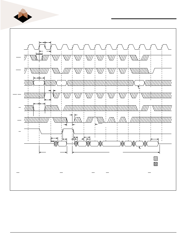
FIG. 3 READ TIMING DIAGRAM
ADSP
ADSC
ADDRESS
BWx, GW
CE
(NOTE 2)
t
ADSS
t
ADSH
ADV
OE
CLOCK
A
2
A
1
t
AS
t
AH
Q
t
AAS
t
AAH
Q(A
2
)
Q(A
2+1
)
t
KH
t
KL
t
KC
t
KQ
Q(A
2+3
)
Q(A
2+1
)
Q(A
1
)
Q(A
2+2
)
t
KQLZ
t
OELZ
t
KQ
t
OEQ
t
OEHZ
SINGLE READ
BURST READ
Q(A
2
)
t
KQHZ
(NOTE 3)
A
3
DON'T CARE
UNDEFINED
Deselect Cycle
(NOTE 4)
ADV suspends burst
t
CSS
t
CSH
t
WS
t
WA
Burst continued with
new base address
Burst wraps around
to its initial state
(NOTE 1)
HIGH-Z
t
KQX
NOTES:
1. Q (A
2
) refers to output from address A
2
. Q (A
2
+1) refers to output from the next internal burst address following A
2
.
2. CE
2
and CE
2
have timing identical to CE. On this diagram, when CE is LOW, CE
2
is LOW and CE
2
is HIGH. When CE is HIGH, CE
2
is
HIGH and CE
2
is LOW.
3. Timing is shown assuming that the device was not enabled before entering into this sequence. OE does not cause Q to be driven until
after the following clock rising edge.
4. Outputs are disabled within one clock cycle after deselect.
8
White Electronic Designs Corporation Westborough MA (508) 366-5151
White Electronic Designs
WED2DL36513V
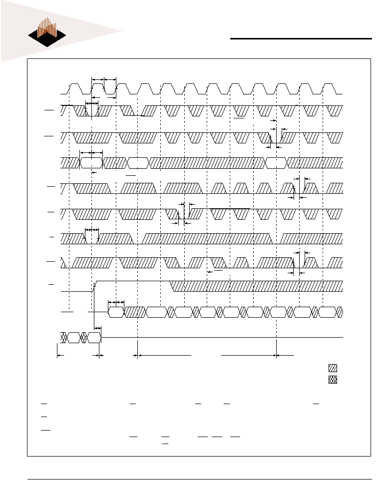
FIG. 4 WRITE TIMING DIAGRAM
ADSP
ADSC
ADDRESS
BWx
CE
(NOTE 2)
t
ADSS
t
ADSH
ADV
OE
CLOCK
A
2
A
1
t
AS
t
AH
Q
t
AAS
t
AAH
t
KH
t
KL
t
KC
t
OEHZ
BURST READ
SINGLE WRITE
BURST WRITE
Extended BURST WRITE
(NOTE 5)
A
3
DON'T CARE
UNDEFINED
(NOTE 3)
ADV suspends burst
t
CSS
t
CSH
t
WS
t
WA
ADSC extends burst
BYTE WRITE signals are ignored for
first cycle when ADSP initiates burst.
(NOTE 1)
D
D(A
1
)
D(A
2
)
D(A
2+1
)
D(A
2+1
)
D(A
2+2
)
D(A
2+3
)
D(A
3
)
D(A
3+1
)
HIGH-Z
t
ADSS
t
ADSH
GW
t
WH
(NOTE 3)
(NOTE 5)
t
WS
(NOTE 4)
D(A
3+2
)
t
DS
t
DH
NOTES:
1. D (A
2
) refers to output from address A
2
. D (A
2+1
) refers to output from the next internal burst address following A
2
.
2. CE
2
and CE
2
have timing identical to CE. On this diagram, when CE is LOW, CE
2
is LOW and CE
2
is HIGH. When CE is HIGH, CE
2
is
HIGH and CE
2
is LOW.
3. OE must be HIGH before the input data setup and held HIGH throughout the data hold time. This prevents input/output data content in
for the time period prior to the byte write enable inputs being sampled.
4. ADV must be HIGH to permit a WRITE to the load address.
5. Full-width WRITE can be initiated by GW LOW, or GW HIGH and BWE, BWa, - BWd LOW. Timing is shown assuming that the device
was not enabled before entering into its sequence. OE does not cause Q to be driven until after the following clock rising edge.
9
White Electronic Designs Corporation (508) 366-5151 www.whiteedc.com
White Electronic Designs
WED2DL36513V
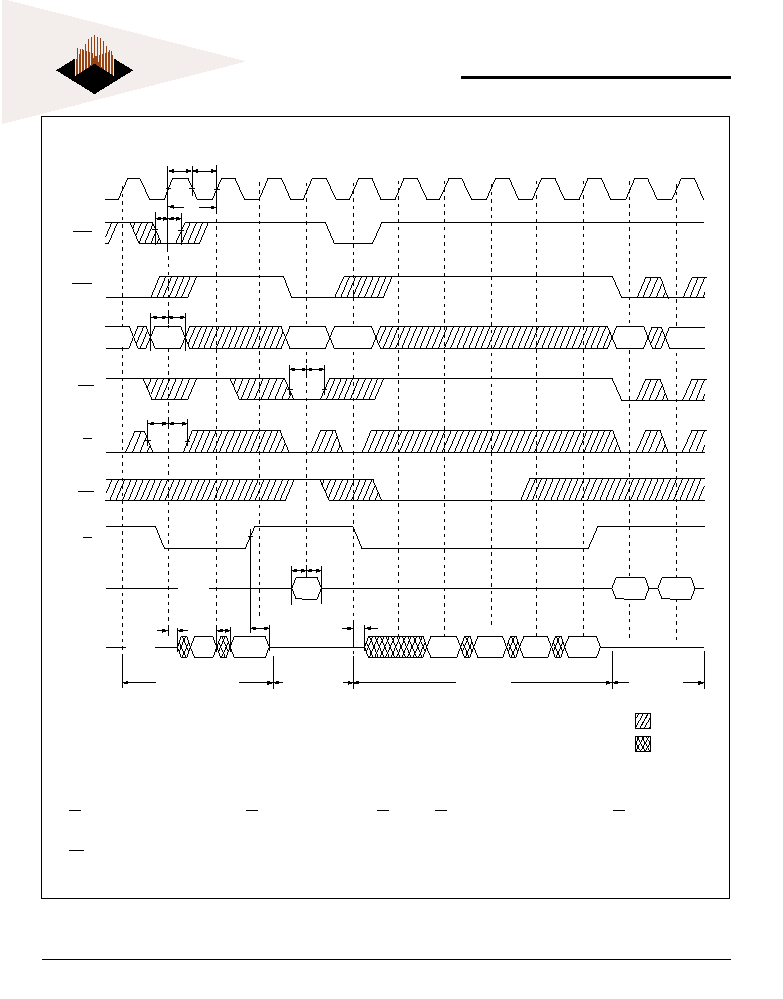
FIG. 5 READ/WRITE TIMING DIAGRAM
ADSP
ADSC
ADDRESS
BWx
(NOTE 4)
CE
(NOTE 2)
t
ADSS
t
ADSH
ADV
OE
CLOCK
A
2
t
AS
t
AH
Q
t
KH
t
KL
t
KC
t
OELZ
Q(A
4+2
)
Q(A
4
)
Q(A
1
)
Q(A
4+1
)
Q(A
4+3
)
t
KQLZ
t
KQ
t
OEHZ
Back-to-Back READs
(NOTE5)
SINGLE WRITE
Back-to-Back
WRITEs
BURST READ
Q(A
2
)
(NOTE 3)
A
5
A
6
DON'T CARE
UNDEFINED
t
CSS
t
CSH
t
WS
t
WH
(NOTE 1)
HIGH-Z
D
HIGH-Z
A
1
A
3
A
4
(NOTE 4)
D(A
3
)
D(A
5
)
D(A
6
)
t
DS
t
DH
NOTES:
1. Q (A
4
) refers to output from address A
4
. Q (A
4+1
) refers to output from the next internal burst address following A
4
.
2. CE
2
and CE
2
have timing identical to CE. On this diagram, when CE is LOW, CE
2
is LOW and CE
2
is HIGH. When CE is HIGH, CE
2
is
HIGH and CE
2
is LOW.
3. The data bus Q remains in High-Z following a WRITE cycle unless ADSP, ADSC or ADV cycle is performed.
4. GW is HIGH.
5. Back-to-back READs may be controlled by either ADSP or ADSC.
10
White Electronic Designs Corporation Westborough MA (508) 366-5151
White Electronic Designs
WED2DL36513V
O
RDERING
I
NFORMATION
512Kx36, Single CE
Part Number
Config.
t
KQ
Clock Package
(ns) (MHz)
No.
Commercial Temp Range (0�C to 70�C)
WED2DL36513V25BC
512Kx36
2.5
200
435
WED2DL36513V35BC
512Kx36
3.5
166
435
WED2DL36513V38BC
512Kx36
3.8
150
435
WED2DL36513V40BC
512Kx36
4.0
133
435
Industrial Temp Range (-40�C to +85�C)*
WED2DL36513V38BI
512Kx36
3.8
150
435
WED2DL36513V40BI
512Kx36
4.0
133
435
* Advanced Information
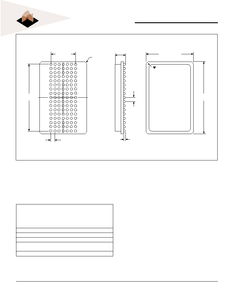
PACKAGE DIMENSION: 119 BUMP PBGA
2.79 (0.110)
MAX
0.711 (0.028)
MAX
1.27 (0.050)
TYP
1.27 (0.050) TYP
A
B
C
D
E
F
G
H
J
K
L
M
N
P
R
T
U
14.00 (0.551) TYP
A1
CORNER
20.32 (0.800)
TYP
22.00 (0.866)
TYP
7.62 (0.300)
TYP
R 1.52 (0.060)
MAX (4x)
7
6
5
4
3
2
1
ALL LINEAR DIMENSIONS ARE MILLIMETERS AND PARENTHETICALLY IN INCHES
NOTE: Ball attach pad for above BGA package is 480 microns in diameter. Pad is solder mask defined.