
1
White Electronic Designs Corporation ∑ (602) 437-1520 ∑ www.wedc.com
White Electronic Designs
WED2EG472512V-D2
Jan, 2000
Rev. A
ADVANCED*
White Electronic Designs Corp. reserves the right to change products or specifi cations without notice.
4x512Kx72 Synchronous Burst
Pipeline Architecture; Dual Cycle Deselect
Linear and Sequential Burst Support via MODE pin
Clock Controlled Registered Module Enable (EM#)
Clock Controlled Registered Bank Enables (E1#,
E2#, E3#, E4#)
Clock Controlled Byte Write Mode Enable (BWE#)
Clock Controlled Byte Write Enables
(BW1#-BW8#)
Clock Controlled Registered Address
Clock Controlled Registered Global Write (GW#)
Asynchronous Output Enable (G#)
Internally Self-Timed Write
Individual Bank Sleep Mode Enables (ZZ1, ZZ2,
ZZ3, ZZ4)
Gold Lead Finish
3.3V ± 10% Operation
Frequency(s): 200, 166, 150 and 133MH
Z
Access Apeed(s): t
KHQV
= 3.0, 3.5, 3.7 and 4.0ns
Common
Data
I/O
High Capacitance (30pF) Drive, at Rated Access
Speed
Single Total Array Clock
Multiple V
CC
and G
ND
for Improved Noise Immunity
16MB (4x512Kx72) SYNC BURST PIPELINE,
DUAL KEY DIMM
DESCRIPTION
FEATURES
The WED2EG472512V is a Synchronous/Synchronous
Burst SRAM, 84 position Dual Key; Double High DIMM
(168 contacts) Module, organized as 4x512Kx72. The
Module contains sixteen (16) Synchronous Burst RAM
devices, packaged in the industry standard JEDEC
14mmx20mm TQFP placed on a Multilayer FR4 Substrate.
The Module Architecture is defi ned as a Sync/SyncBurst,
Pipeline, with support for either linear or sequential burst.
This Module provides high performance, 3-1-1-1 accesses
when used in Burst Mode.
Synchronous Only operations are performed via strapping
ADSC# Low, and ADSP#/ADV# High, which provides for
Ultra Fast Accesses in Read Mode while providing for
internally self-timed Early Writes.
Synchronous/Synchronous Burst operations are in relation
to an externally supplied clock, Registered Address,
Registered Global Write, egistered Enables as well as
an Asynchronous Output Enable. This module has been
defi ned with full fl exibility, which allowes individual control
of each of the eight bytes, as well as Quad Words in both
Read and Write Operations.
* This product is under development, is not qualifi ed or characterized and is subject to
change or cancellation without notice.
2
White Electronic Designs Corporation ∑ (602) 437-1520 ∑ www.wedc.com
White Electronic Designs
WED2EG472512V-D2
Jan, 2000
Rev. A
ADVANCED
White Electronic Designs Corp. reserves the right to change products or specifi cations without notice.
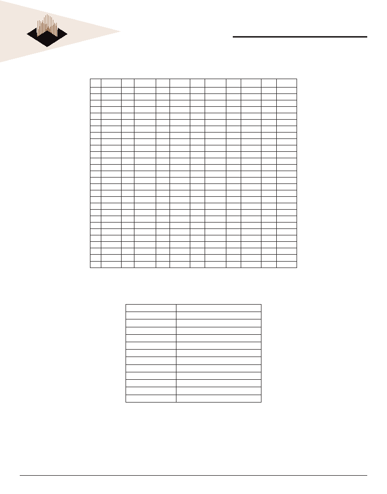
Pin
Front
Pin
Front
Pin
Front
Pin
Back
Pin
Back
Pin
Back
1
V
SS
29
NC
57
NC
85
V
SS
113
DQP0
141
DQP4
2
A0
30
V
CC
58
V
CC
86
A17
114
V
CC
142
V
CC
3
A16
31
DQ0
59
DQ32
87
A1
115
DQ7
143
DQ39
4
A2
32
DQ1
60
DQ33
88
A15
116
DQ6
144
DQ38
5
A14
33
DQ2
61
DQ34
89
A3
117
DQ5
145
DQ37
6
V
CC
34
DQ3
62
DQ35
90
V
CC
118
DQ4
146
DQ36
7
A4
35
V
SS
63
V
SS
91
A13
119
V
SS
147
V
SS
8
A12
36
ZZ1
64
ZZ3
92
A5
120
DQP1
148
DQP5
9
A6
37
V
CC
65
V
CC
93
A11
121
V
CC
149
V
CC
10
A10
38
DQ8
66
DQ40
94
A7
122
DQ15
150
DQ47
11
V
SS
39
DQ9
67
DQ41
95
V
SS
123
DQ14
151
DQ46
12
A8
40
DQ10
68
DQ42
96
A9
124
DQ13
152
DQ45
13
RFU
41
DQ11
69
DQ43
97
A18
125
DQ12
153
DQ44
14
E4#
42
V
SS
70
V
CC
98
E1#
126
V
SS
154
V
SS
15
E2#
43
NC
71
NC
99
E3#
127
DQP2
155
DQP6
16
V
SS
44
V
CC
72
V
CC
100
V
SS
128
V
CC
156
V
CC
17
MODE
45
DQ16
73
DQ48
101
CK
129
DQ23
157
DQ55
18
EM#
46
DQ17
74
DQ49
102
V
SS
130
DQ22
158
DQ54
19
GW#
47
DQ18
75
DQ50
103
G#
131
DQ21
159
DQ53
20
RFU
48
DQ19
76
DQ51
104
BWE#
132
DQ20
160
DQ52
21
V
CC
49
V
SS
77
V
SS
105
V
CC
133
V
SS
161
V
SS
22
BW4#
50
ZZ2
78
ZZ4
106
BW2#
134
DQP3
162
DQP7
23
BW3#
51
V
CC
79
V
CC
107
BW1#
135
V
CC
163
V
CC
24
BW8#
52
DQ24
80
DQ56
108
BW6#
136
DQ31
164
DQ63
25
BW7#
53
DQ25
81
DQ57
109
BW5#
137
DQ30
165
DQ62
26
ADSC#
54
DQ26
82
DQ58
110
V
SS
138
DQ29
166
DQ61
27
ADSP#
55
DQ27
83
DQ59
111
ADV#
139
DQ28
167
DQ60
28
V
SS
56
V
SS
84
V
SS
112
V
SS
140
V
SS
168
V
SS
PIN CONFIGURATION
DQ0 - DQ63
Input / Output Bus
DQP0 - DQP7
Parity Bits
A0 - A18
Address Bus
EM#
Module Enable
E1#, E2#, E3#, E4#
Synchronous Bank Enables
BWE#
Byte Write Mode Enable
BW1# - BW8#
Byte Write Enables
CK
Array Clock
GW#
Synchronous Global Write Enable
G#
Asynchronous Output Enable
ZZ1, ZZ2, ZZ3, ZZ4
Bank Sleep Mode Enables
V
CC
3.3V Power Supply
V
SS
Ground
PIN DESCRIPTION
3
White Electronic Designs Corporation ∑ (602) 437-1520 ∑ www.wedc.com
White Electronic Designs
WED2EG472512V-D2
Jan, 2000
Rev. A
ADVANCED
White Electronic Designs Corp. reserves the right to change products or specifi cations without notice.
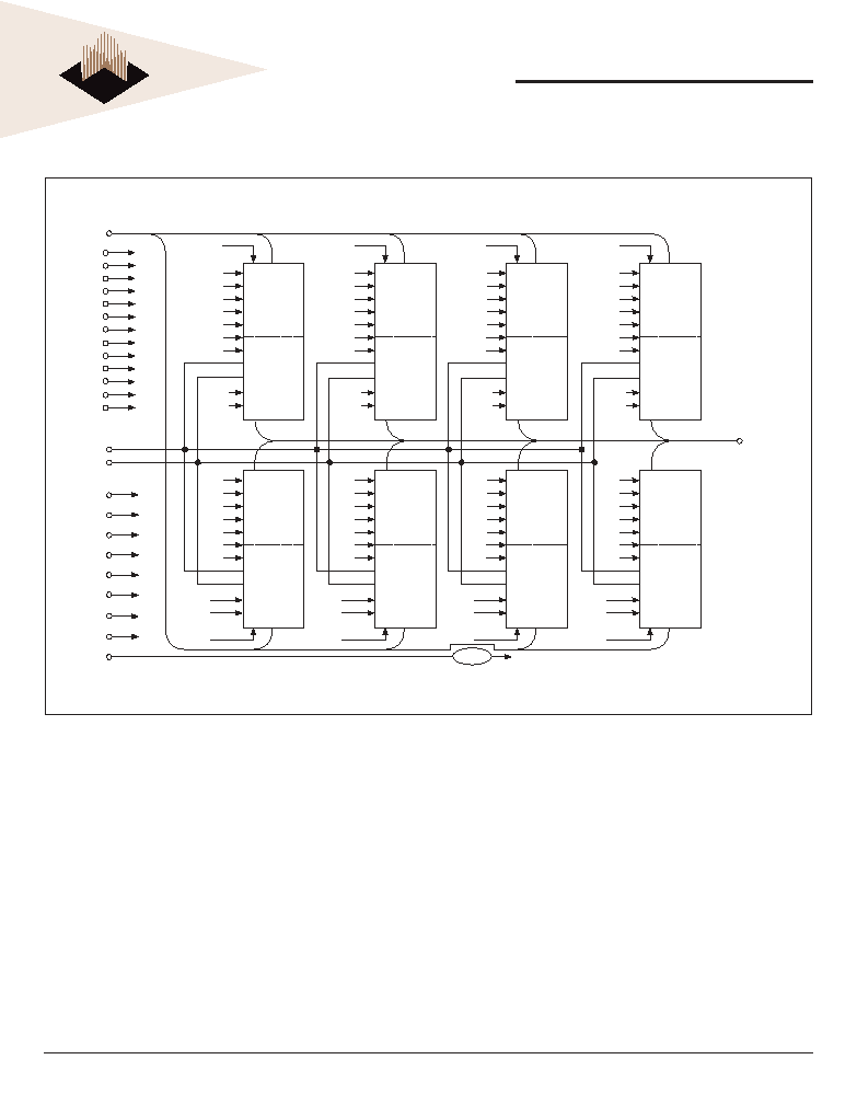
FUNCTIONAL BLOCK DIAGRAM
ADDR
BW
8#
BW
7#
BW
6#
BW
5#
BW
4#
BW
3#
BW
2#
BW
1#
BWE#
E
4#
E
3#
E
2#
E
1#
ADV#
BW
4#
BW
3#
BW
2#
BW
1#
BWE#
ADSP#
ADSC#
512K x 18
SBPL
DCD
512K x 18
SBPL
DCD
MODE
ADSP#
ADSC#
ADV#
ZZ
1
ZZ
2
ZZ
3
ZZ
4
CK
BW
8#
BW
7#
BW
6#
BW
5#
BW
4#
BW
3#
BW
2#
BW
1#
BWE#
E
4#
E
3#
E
2#
E
1#
GW#
G#
E
1#
ZZ
1
GW#
G#
BW
8#
BW
7#
BW
6#
BW
5#
BWE#
ADSP#
ADSC#
ADV#
512K x 18
SBPL
DCD
512K x 18
SBPL
DCD
E
1#
ZZ
1
GW#
G#
ADV#
BW
4#
BW
3#
BW
2#
BW
1#
BWE#
ADSP#
ADSC#
512K x 18
SBPL
DCD
512K x 18
SBPL
DCD
E
2#
ZZ
2
GW#
G#
BW
8#
BW
7#
BW
6#
BW
5#
BWE#
ADSP#
ADSC#
ADV#
512K x 18
SBPL
DCD
512K x 18
SBPL
DCD
E
2#
ZZ
2#
GW#
G#
ADV#
BW
4#
BW
3#
BW
2#
BW
1#
BWE#
ADSP#
ADSC#
512K x 18
SBPL
DCD
512K x 18
SBPL
DCD
E
3#
ZZ
3
GW#
G#
BW
8#
BW
7#
BW
6#
BW
5#
BWE#
ADSP#
ADSC#
ADV#
512K x 18
SBPL
DCD
512K x 18
SBPL
DCD
E
3#
ZZ
3
GW#
G#
ADV#
BW
4#
BW
3#
BW
2#
BW
1#
BWE#
ADSP#
ADSC#
512K x 18
SBPL
DCD
512K x 18
SBPL
DCD
E
4#
ZZ
4
GW#
G#
BW
8#
BW
7#
BW
6#
BW
5#
BWE#
ADSP#
ADSC#
ADV#
512K x 18
SBPL
DCD
512K x 18
SBPL
DCD
E
4#
ZZ
4
GW#
G#
U1 -U8 EQUAL LENGTH NET ROUTES
Data (DQ)
4
White Electronic Designs Corporation ∑ (602) 437-1520 ∑ www.wedc.com
White Electronic Designs
WED2EG472512V-D2
Jan, 2000
Rev. A
ADVANCED
White Electronic Designs Corp. reserves the right to change products or specifi cations without notice.
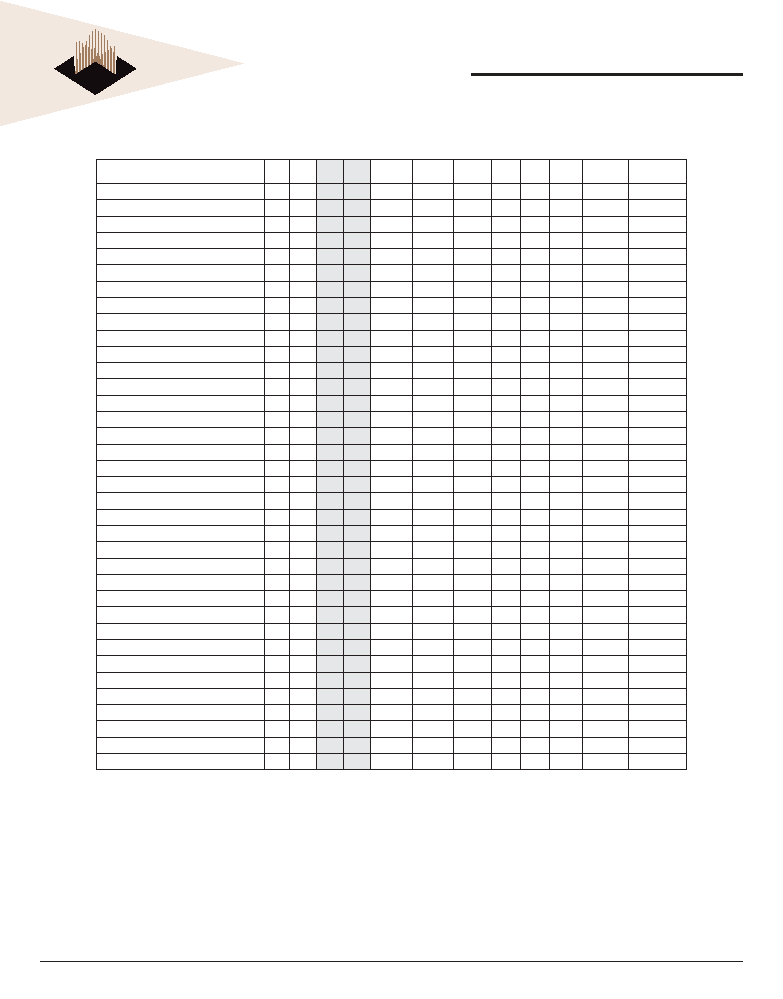
SYNC BURST - TRUTH TABLE
Note A : All truth Table Functions Repeat for Bank 3 (E3#)and Bank 4 (E4#).
Operation
E1#
E2#
E3#
E4#
ADSP#
ADSC#
ADV#
GW#
G#
CK
DQ
Addr. Used
Deselected Cycle, Power Down; Bank 1
H
X
X
L
X
X
X
L-H
High-Z
None
Deselected Cycle, Power Down; Bank 2
X
H
X
L
X
X
X
L-H
High-Z
None
Read Cycle, Begin Burst; Bank 1
L
H
L
X
X
X
L
L-H
Q
External
Read Cycle, Begin Burst; Bank 1
L
H
L
X
X
X
H
L-H
High-Z
External
Read Cycle, Begin Burst; Bank 2
H
L
L
X
X
X
L
L-H
Q
External
Read Cycle, Begin Burst; Bank 2
H
L
L
X
X
X
H
L-H
High-Z
External
Write Cycle, Begin Burst; Bank 1
L
H
H
L
X
L
X
L-H
D
External
Write Cycle, Begin Burst; Bank 2
H
L
H
L
X
L
X
L-H
D
External
Read Cycle, Begin Burst; Bank 1
L
H
H
L
X
H
L
L-H
Q
External
Read Cycle, Begin Burst; Bank 1
L
H
H
L
X
H
H
L-H
High-Z
External
Read Cycle, Begin Burst; Bank 2
H
L
H
L
X
H
L
L-H
Q
External
Read Cycle, Begin Burst; Bank 2
H
L
H
L
X
H
H
L-H
High-Z
External
Read Cycle, Continue Burst; Bank 1
X
H
X
H
L
H
L
L-H
Q
Next
Read Cycle, Continue Burst; Bank 1
X
H
X
H
L
H
H
L-H
High-Z
Next
Read Cycle, Continue Burst; Bank 2
H
X
X
H
L
H
L
L-H
Q
Next
Read Cycle, Continue Burst; Bank 2
H
X
X
H
L
H
H
L-H
High-Z
Next
Read Cycle, Continue Burst; Bank 1
H
H
X
H
L
H
L
L-H
Q
Next
Read Cycle, Continue Burst; Bank 1
H
H
X
H
L
H
H
L-H
High-Z
Next
Read Cycle, Continue Burst; Bank 2
H
H
X
H
L
H
L
L-H
Q
Next
Read Cycle, Continue Burst; Bank 2
H
H
X
H
L
H
H
L-H
High-Z
Next
Write Cycle, Continue Burst; Bank 1
X
H
H
H
L
L
X
L-H
D
Next
Write Cycle, Continue Burst; Bank 1
H
H
X
H
L
L
X
L-H
D
Next
Write Cycle, Continue Burst; Bank 2
H
X
H
H
L
L
X
L-H
D
Next
Write Cycle, Continue Burst; Bank 2
H
H
X
H
L
L
X
L-H
D
Next
Read Cycle, Suspend Burst; Bank 1
X
H
H
H
H
H
L
L-H
Q
Current
Read Cycle, Suspend Burst; Bank 1
X
H
H
H
H
H
H
L-H
High-Z
Current
Read Cycle, Suspend Burst; Bank 2
H
X
H
H
H
H
L
L-H
Q
Current
Read Cycle, Suspend Burst; Bank 2
H
X
H
H
H
H
H
L-H
High-Z
Current
Read Cycle, Suspend Burst; Bank 1
H
H
X
H
H
H
L
L-H
Q
Current
Read Cycle, Suspend Burst; Bank 1
H
H
X
H
H
H
H
L-H
High-Z
Current
Read Cycle, Suspend Burst; Bank 2
H
H
X
H
H
H
L
L-H
Q
Current
Read Cycle, Suspend Burst; Bank 2
H
H
X
H
H
H
H
L-H
High-Z
Current
Write Cycle, Suspend Burst; Bank 1
X
H
H
H
H
L
X
L-H
D
Current
Write Cycle, Suspend Burst; Bank 1
H
H
X
H
H
L
X
L-H
D
Current
Write Cycle, Suspend Burst; Bank 2
H
X
H
H
H
L
X
L-H
D
Current
Write Cycle, Suspend Burst; Bank 2
H
H
X
H
H
L
X
L-H
D
Current
Note A
5
White Electronic Designs Corporation ∑ (602) 437-1520 ∑ www.wedc.com
White Electronic Designs
WED2EG472512V-D2
Jan, 2000
Rev. A
ADVANCED
White Electronic Designs Corp. reserves the right to change products or specifi cations without notice.
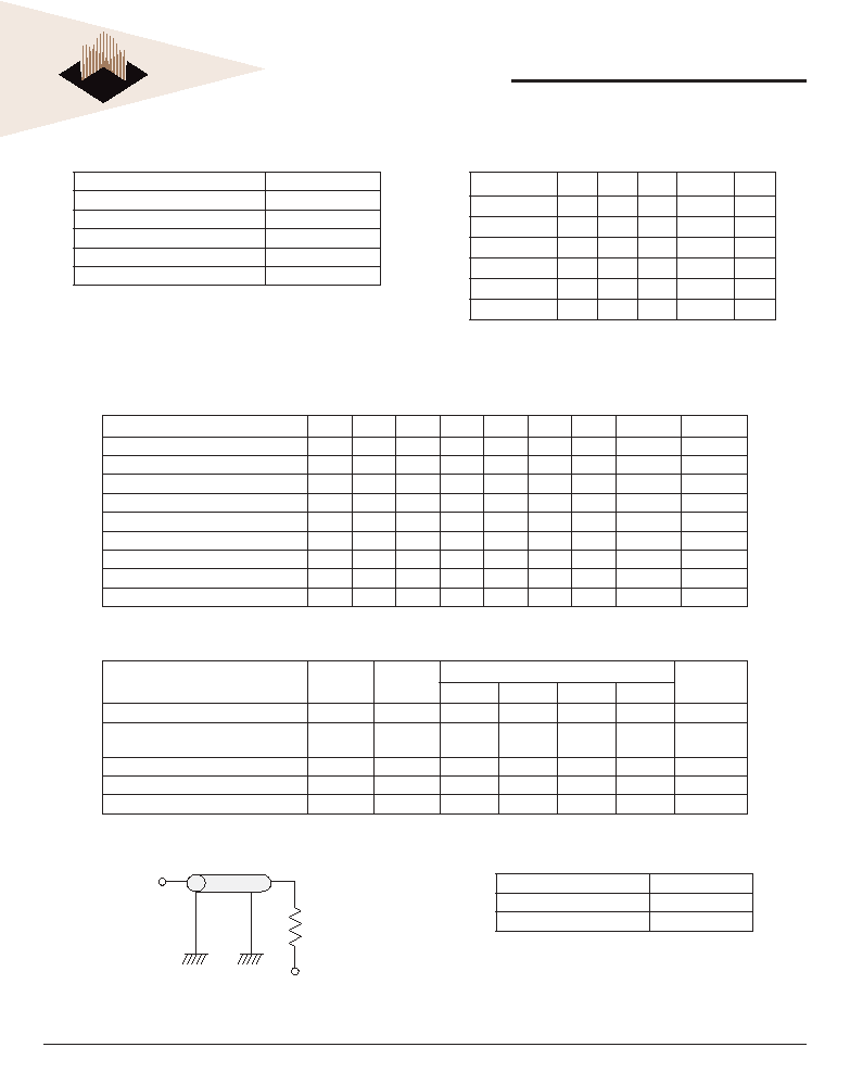
ABSOLUTE MAXIMUM RATINGS*
RECOMMENDED DC OPERATING CONDITIONS
Voltage on V
CC
Relative to V
SS
-0.3V to +4.6V
V
IN
-0.3V to V
CC
+0.5V
Storage Temperature
-55∞C to +125∞C
Operating Temperature (Commercial)
0∞C to +70∞C
Operating Temperature (Industrial)
-40∞C to +85∞C
Short Circuit Output Current
100mA
Parameter
Sym
Min
Typ
Max
Units
Supply Voltage
V
CC
3.3
3.3
3.6
V
Supply Voltage
V
SS
0
0
0
V
Input High
V
IH
2.0
3.0
V
CC
+ 0.3
V
Input Low
V
IL
-0.3
0
0.3
V
Input Leakage
I
LI
-2
1
3
µA
Output Leakage
I
LO
-2
1
2
µA
* Stress greater than those listed under "Absolute Maxamin Ratings" may cause
permanent damage to the device. This is a stress rating only and functional operation
of the device at these or any other conditions greater than those indicated in the
operational sections of this specifi cation is not implied. Exposure to absolute maximum
rating conditions for extended periods may effect reliability
SYNCHRONOUS ONLY - TRUTH TABLE
Operation
E1#
E2#
E3#
E4#
GW#
G#
ZZ
CK
DQ
Synchronous Write - Bank 1
L
H
H
H
L
H
L
High-Z
Synchronous Read - Bank 1
L
H
H
H
H
L
L
Synchronous Write - Bank 2
H
L
H
H
L
H
L
High-Z
Synchronous Read - Bank 2
H
L
H
H
H
L
L
Synchronous Write - Bank 3
H
H
L
H
L
H
L
High-Z
Synchronous Read - Bank 3
H
H
L
H
H
L
L
Synchronous Write - Bank 4
H
H
H
L
L
H
L
High-Z
Synchronous Read - Bank 4
H
H
H
L
H
L
L
Snooze Mode
X
X
X
X
X
X
H
X
High-Z
DC ELECTRICAL CHARACTERISTICS READ CYCLE
Description
Sym
Typ
Max
Units
5.0
6.0
6.5
7.0
Power Supply Current
I
CC1
1.8
2.6
2.4
2.3
2.2
A
Power Supply Current
Device Selected, No Operation
I
CC
875
1.8
1.8
1.3
1.3
A
Snooze Mode
I
CCZZ
270
350
350
350
350
mA
CMOS Standby
I
CC3
500
700
700
700
700
mA
Clock Running-Deselect
I
CCK
900
1.1
1.1
1.0
1.0
A
AC TEST LOAD
RL = 50
VL = 1.25V
DQ Output
Z0 = 50
Output Test Equivalencies
AC TEST CONDITIONS
Input Pulse Levels
V
SS
to 3.0V
Input and Output Timing Ref.
1.25V
Output test Equivalencies
see fi gure at left

6
White Electronic Designs Corporation ∑ (602) 437-1520 ∑ www.wedc.com
White Electronic Designs
WED2EG472512V-D2
Jan, 2000
Rev. A
ADVANCED
White Electronic Designs Corp. reserves the right to change products or specifi cations without notice.
SYNC-BURST READ CYCLE PARAMETERS
Description
Sym
3.0ns
3.5ns
3.7ns
4.0ns
Units
Min
Max
Min
Max
Min
Max
Min
Max
Frequency
f
MAX
200
160
150
133
MH
Z
Clock Cycle Time
t
KC
5.0
6.0
6.5
7.0
ns
Clock High Time
t
KH
2
2.4
2.5
3
ns
Clock Low Time
t
KL
2
2.4
2.5
3
ns
Clock to Output Valid
t
KQ
3
3.5
3.7
4
ns
Clock to Output Invalid
t
KQX
1.25
1.25
1.25
1.25
ns
Clock to Output Low-Z
t
KQLZ
0
0
0
0
ns
Clock Enable to Output Valid
t
OEQ
1.25
3
1.25
4
1.25
4
1.25
5
ns
Clock Enable to Output Low-Z
t
OELZ
0
0
0
0
ns
Clock Enable to Output High-Z
t
OEHZ
2.5
3.5
3.5
4
ns
Address Setup
t
S
1.5
1.5
1.8
2.0
ns
Bank Enable Setup
t
S
1.5
1.5
1.8
2.0
ns
Address Hold
t
H
0.5
0.5
0.5
0.5
ns
Bank Enable Hold
t
H
0.5
0.5
0.5
0.5
ns
SYNC-BURST WRITE CYCLE PARAMETERS
Description
Sym
3.0ns
3.5ns
3.7ns
4.0ns
Units
Min
Max
Min
Max
Min
Max
Min
Max
Frequency
f
MAX
200
166
150
133
MH
Z
Clock Cycle Time
t
KC
5.0
6.0
6.5
7.0
ns
Clock High Time
t
KH
2
2.4
2.7
3
ns
Clock Low Time
t
KL
2
2.4
2.7
3
ns
Address Setup
tS
1.5
1.5
1.8
2.0
ns
Address Hold
tH
0.5
0.5
0.5
0.5
ns
Bank Enable Setup
tS
1.5
1.5
1.8
1.8
ns
bank Enable Hold
tH
0.5
0.5
0.5
0.5
ns
Global Write Enable Setup
tS
1.5
1.5
1.8
1.8
ns
Global Write Enable Hold
tH
0.5
0.5
0.5
0.5
ns
Data Setup
tS
1.5
1.5
1.8
1.8
ns
Data Hold
tH
0.5
0.5
0.5
0.5
ns
7
White Electronic Designs Corporation ∑ (602) 437-1520 ∑ www.wedc.com
White Electronic Designs
WED2EG472512V-D2
Jan, 2000
Rev. A
ADVANCED
White Electronic Designs Corp. reserves the right to change products or specifi cations without notice.
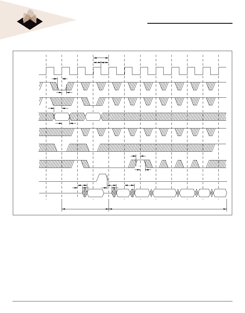
SYNC-BURST READ CYCLE
Burst Read
Single Read
t
KQ
t
KQLZ
DQx
G#
EM#, E#
ADV#
BWx#,
BWE#, GW#
t
OEQ
t
KQ
t
OELZ
t
KC
t
S
t
H
t
H
ADSP#
Ax
ADSC#
CK
t
KL
t
KH
A
2
Q(A
1
)
Q(A
2
)
Q(A
2+1
)
A
1
t
S
t
H
Q(A
2+2
)
Q(A
2+3
)
Q(A
2+1
)
Q(A
2
)
t
S
8
White Electronic Designs Corporation ∑ (602) 437-1520 ∑ www.wedc.com
White Electronic Designs
WED2EG472512V-D2
Jan, 2000
Rev. A
ADVANCED
White Electronic Designs Corp. reserves the right to change products or specifi cations without notice.
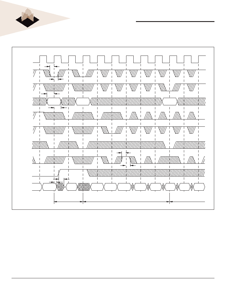
SYNC-BURST WRITE CYCLE
Burst Write
Burst Write
Single Write
t
OEHZ
t
KQX
DQx
G#
EM#, E#
ADV#
BWx#,
BWE#
t
S
t
H
t
H
ADSP#
Ax
ADSC#
CK
GW#
A
2
A
3
D(A
1
)
D(A
2
)
D(A
2+1
)
D(A
2+1
)
Q
A
1
t
S
t
H
D(A
2+2
)
D(A
2+3
)
D(A
3+1
)
D(A
3
)
D(A
3+2
)
t
S

9
White Electronic Designs Corporation ∑ (602) 437-1520 ∑ www.wedc.com
White Electronic Designs
WED2EG472512V-D2
Jan, 2000
Rev. A
ADVANCED
White Electronic Designs Corp. reserves the right to change products or specifi cations without notice.
SYNC-BURST READ/WRITE CYCLE
Burst Read
Burst Write
Single Read
Single Write
DQx
G#
EM#, E#
ADV#
BWx#,
BWE#,
GW#
t
S
t
H
t
H
ADSP#
Ax
ADSC#
CK
A
3
A
4
A
5
D(A
3
)
Q(A
1
)
A
1
A
2
t
S
Q(A
4
)
Q(A
4+1
)
D(A
5
)
Q(A
4+2
)
D(A
5+1
)
Q(A
2
)
10
White Electronic Designs Corporation ∑ (602) 437-1520 ∑ www.wedc.com
White Electronic Designs
WED2EG472512V-D2
Jan, 2000
Rev. A
ADVANCED
White Electronic Designs Corp. reserves the right to change products or specifi cations without notice.
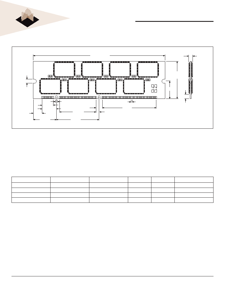
PACKAGE DIMENSIONS: 168 DUAL KEY DIMM
P1
195
0.157
(2x)
0.078 (2X)
0.450
0.350
0.925
1.450
0.250
0.125
1.700
2.150
0.050 TYP.
0.700
MAX.
MAX.
1.500
0.195
0.575
MIN.
0.225
5.255 MAX.
ALL DIMENSIONS ARE IN INCHES
ORDERING INFORMATION
Part Number
Confi guration
Description
Voltage (V)
Frequency
Package
WED2EG472512V5D2
16MB (4 x 512K x 72)
Sync-Burst Pipeline
3.3
200MH
Z
168 Dual Key DIMM
WED2EG472512V6D2
16MB (4 x 512K x 72)
Sync-Burst Pipeline
3.3
166MH
Z
168 Dual Key DIMM
WED2EG472512V65D2
16MB (4 x 512K x 72)
Sync-Burst Pipeline
3.3
150MH
Z
168 Dual Key DIMM
WED2EG472512V7D2
16MB (4 x 512K x 72)
Sync-Burst Pipeline
3.3
133MH
Z
168 Dual Key DIMM