1
1
1
1
1
White Electronic Designs Corporation ∑ (508) 366-5151 ∑ www.whiteedc.com
White Electronic Designs
WED2ZL236512S
WED2ZL236512S
WED2ZL236512S
WED2ZL236512S
WED2ZL236512S
1
1
1
1
1
2
2
2
2
2
3
3
3
3
3
4
4
4
4
4
5
5
5
5
5
6
6
6
6
6
7
7
7
7
7
A
A
A
A
A
V
DD
SA
SA
SA
SA
SA
V
DD
B
B
B
B
B
SA
CE
A
SA
ADV
SA
CE
B
DNC
C
C
C
C
C
NC
SA
SA
V
DD
SA
SA
DNC
D
D
D
D
D
DQ
C
DQP
C
V
SS
DNC
V
SS
DQP
B
DQ
B
E
E
E
E
E
DQ
C
DQ
C
V
SS
DNC
V
SS
DQ
B
DQ
B
F
F
F
F
F
V
DD
DQ
C
V
SS
OE
V
SS
DQ
B
V
DD
G
G
G
G
G
DQ
C
DQ
C
BW
C
DNC
BW
B
DQ
B
DQ
B
H
H
H
H
H
DQ
C
DQ
C
V
SS
WE
V
SS
DQ
B
DQ
B
J
J
J
J
J
V
DD
V
DD
DNC
V
DD
DNC
V
DD
V
DD
K
K
K
K
K
DQ
D
DQ
D
V
SS
CLK
V
SS
DQ
A
DQ
A
L
L
L
L
L
DQ
D
DQ
D
BW
D
NC
BW
A
DQ
A
DQ
A
M
M
M
M
M
V
DD
DQ
D
V
SS
CKE
V
SS
DQ
A
V
DD
N
N
N
N
N
DQ
D
DQ
D
V
SS
SA
1
V
SS
DQ
A
DQ
A
P
P
P
P
P
DQ
D
DQP
D
V
SS
SA
0
V
SS
DQP
A
DQ
A
R
R
R
R
R
DNC
SA
LBO
V
DD
NC
SA
NC
T
T
T
T
T
DNC
NC
SA
SA
SA
NC
ZZ
U
U
U
U
U
V
DD
NC
NC
NC
NC
NC
VDD
January 2002, Rev. 4
ECO #14644
DESCRIPTION
DESCRIPTION
DESCRIPTION
DESCRIPTION
DESCRIPTION
The WEDC SyncBurst - SRAM family employs high-speed,
low-power CMOS designs that are fabricated using an ad-
vanced CMOS process. WEDC's 32Mb SyncBurst SRAMs
integrate two 512K x 36 SRAMs into a single BGA package
to provide 2 x 512K x 36 configuration. All synchronous
inputs pass through registers controlled by a positive-edge-
triggered single-clock input (CLK). The NBL or No Bus La-
tency Memory utilizes all the bandwidth in any combination
of operating cycles. Address, data inputs, and all control
signals except output enable and linear burst order are syn-
chronized to input clock. Burst order control must be tied
"High or Low." Asynchronous inputs include the sleep mode
enable (ZZ). Output Enable controls the outputs at any
given time. Write cycles are internally self-timed and initi-
ated by the rising edge of the clock input. This feature elimi-
nates complex off-chip write pulse generation and pro-
vides increased timing flexibility for incoming signals.
2 x 512K x 36 Synchronous Pipeline Burst NBL SR
2 x 512K x 36 Synchronous Pipeline Burst NBL SR
2 x 512K x 36 Synchronous Pipeline Burst NBL SR
2 x 512K x 36 Synchronous Pipeline Burst NBL SR
2 x 512K x 36 Synchronous Pipeline Burst NBL SRAM
AM
AM
AM
AM
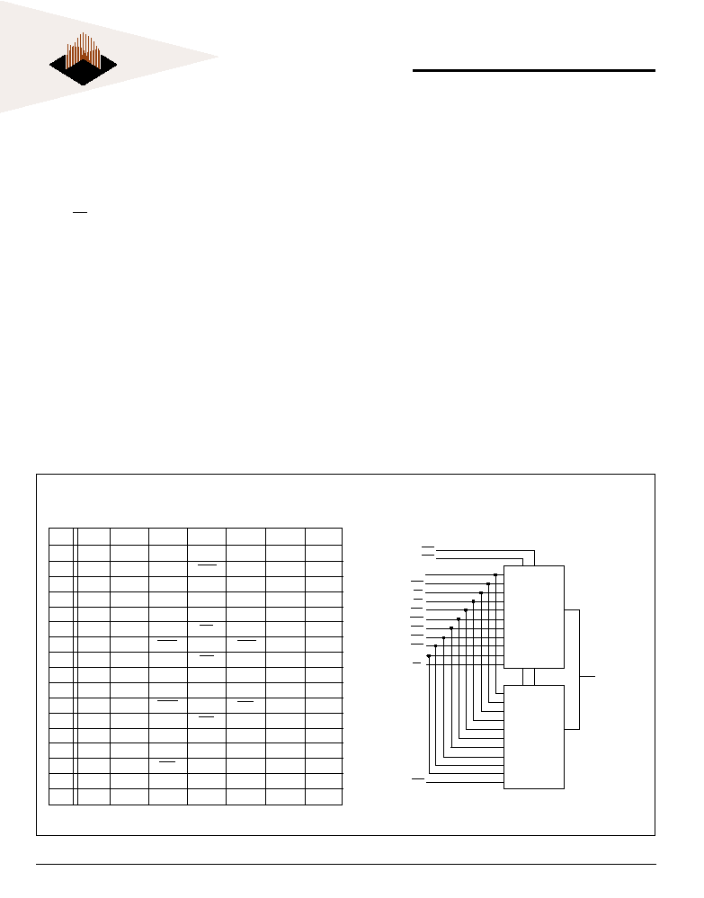
FIG. 1
FIG. 1
FIG. 1
FIG. 1
FIG. 1
BL
BL
BL
BL
BLOCK DIA
OCK DIA
OCK DIA
OCK DIA
OCK DIAGR
GR
GR
GR
GRAM
AM
AM
AM
AM
PIN CONFIGUR
PIN CONFIGUR
PIN CONFIGUR
PIN CONFIGUR
PIN CONFIGURA
A
A
A
ATION
TION
TION
TION
TION
(TOP VIEW)
(TOP VIEW)
(TOP VIEW)
(TOP VIEW)
(TOP VIEW)
CLK
CKE
SA
ADV
OE
WE
BWa
BWb
BWc
BWd
LBO
ZZ
CEa
512K x 36
SSRAM
DQ
a
-
DQ
d
DQPa - DQP
d
512K x 36
SSRAM
CEb
FEA
FEA
FEA
FEA
FEATURES
TURES
TURES
TURES
TURES
!
Fast clock speed: 166, 150, 133, and 100MHz
!
Fast access times: 3.5ns, 3.8ns, 4.0ns, and 5.0ns
!
Fast OE access times: 3.5ns, 3.8ns, 4.0ns, and 5.0ns
!
Single +2.5V ± 5% power supply (VDD)
!
Snooze Mode for reduced-standby power
!
Individual Byte Write control
!
Clock-controlled and registered addresses, data I/Os
and control signals
!
Burst control (interleaved or linear burst)
!
Packaging:
∑ 119-bump BGA package
!
Low capacitive bus loading
Note:
Note:
Note:
Note:
Note:
DNC = Do Not Connect. Connections to these pins may cause the device to not function properly.
2
2
2
2
2
White Electronic Designs Corporation ∑ Westborough, MA ∑ (508) 366-5151
White Electronic Designs
WED2ZL236512S
WED2ZL236512S
WED2ZL236512S
WED2ZL236512S
WED2ZL236512S
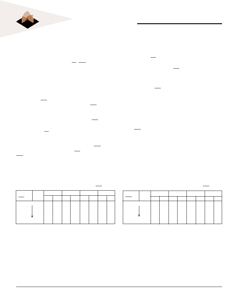
(Linear Burst, LBO = Low)
(Linear Burst, LBO = Low)
(Linear Burst, LBO = Low)
(Linear Burst, LBO = Low)
(Linear Burst, LBO = Low)
Case 1
Case 1
Case 1
Case 1
Case 1
Case 2
Case 2
Case 2
Case 2
Case 2
Case 3
Case 3
Case 3
Case 3
Case 3
Case 4
Case 4
Case 4
Case 4
Case 4
LBO Pin
LBO Pin
LBO Pin
LBO Pin
LBO Pin
High
High
High
High
High
A 1
A 1
A 1
A 1
A 1
A 0
A 0
A 0
A 0
A 0
A 1
A 1
A 1
A 1
A 1
A 0
A 0
A 0
A 0
A 0
A 1
A 1
A 1
A 1
A 1
A 0
A 0
A 0
A 0
A 0
A 1
A 1
A 1
A 1
A 1
A 0
A 0
A 0
A 0
A 0
First Address
0
0
0
1
1
0
1
1
0
1
1
0
1
1
0
0
1
0
1
1
0
0
0
1
Fourth Address
1
1
0
0
0
1
1
0
and the data is latched in the output register. At the sec-
ond clock edge the data is driven out of the SRAM. During
read operation OE must be driven low for the device to
drive out the requested data.
Write operation occurs when WE is driven low at the rising
edge of the clock. BW[
D
:
A
] can be used for byte write
operation. The pipe-lined NBL SSRAM uses a late-late write
cycle to utilize 100% of the bandwidth. At the first rising
edge of the clock, WE and address are registered, and the
data associated with that address is required two cycle
later.
Subsequent addresses are generated by ADV High for the
burst access as shown below. The star ting point of the
burst seguence is provided by the external address. The
burst address counter wraps around to its initial state upon
completion. The burst sequence is determined by the state
of the LBO pin. When this pin is low, linear burst sequence
is selected. And when this pin is high, Interleaved burst
sequence is selected.
During normal operation, ZZ must be driven low. When ZZ
is driven high, the SRAM will enter a Power Sleep Mode
after 2 cycles. At this time, internal state of the SRAM is
preserved. When ZZ returns to low, the SRAM operates
after 2 cycles of wake up time.
BURST SEQUENCE TABLE
BURST SEQUENCE TABLE
BURST SEQUENCE TABLE
BURST SEQUENCE TABLE
BURST SEQUENCE TABLE
NOTE 1: LBO pin must be tied to High or Low, and Floating State must not be allowed.
(Interleaved Burst, LBO = High)
(Interleaved Burst, LBO = High)
(Interleaved Burst, LBO = High)
(Interleaved Burst, LBO = High)
(Interleaved Burst, LBO = High)
Case 1
Case 1
Case 1
Case 1
Case 1
Case 2
Case 2
Case 2
Case 2
Case 2
Case 3
Case 3
Case 3
Case 3
Case 3
Case 4
Case 4
Case 4
Case 4
Case 4
LBO Pin
LBO Pin
LBO Pin
LBO Pin
LBO Pin
High
High
High
High
High
A 1
A 1
A 1
A 1
A 1
A 0
A 0
A 0
A 0
A 0
A 1
A 1
A 1
A 1
A 1
A 0
A 0
A 0
A 0
A 0
A 1
A 1
A 1
A 1
A 1
A 0
A 0
A 0
A 0
A 0
A 1
A 1
A 1
A 1
A 1
A 0
A 0
A 0
A 0
A 0
First Address
0
0
0
1
1
0
1
1
0
1
0
0
1
1
1
0
1
0
1
1
0
0
0
1
Fourth Address
1
1
1
0
0
1
0
0
FUNCTION DESCRIPTION
FUNCTION DESCRIPTION
FUNCTION DESCRIPTION
FUNCTION DESCRIPTION
FUNCTION DESCRIPTION
The WED2ZL263512S is an NBL SSRAM designed to sus-
tain 100% bus bandwidth by eliminating turnaround cycle
when there is transition from Read to Write, or vice versa.
All inputs (with the exception of OE, LBO and ZZ) are syn-
chronized to rising clock edges.
All read, write and deselect cycles are initiated by the ADV
input. Subsequent burst addresses can be internally gen-
erated by the burst advance pin (ADV). ADV should be
driven to Low once the device has been deselected in
order to load a new address for next operation.
Clock Enable (CKE) pin allows the operation of the chip to
be suspended as long as necessary. When CKE is high, all
synchronous inputs are ignored and the internal device
registers will hold their previous values. NBL SSRAM latches
external address and initiates a cycle when CKE and ADV
are driven low at the rising edge of the clock.
Output Enable (OE) can be used to disable the output at
any given time. Read operation is initiated when at the ris-
ing edge of the clock, the address presented to the ad-
dress inputs are latched in the address register, CKE is driven
low, the write enable input signals WE are driven high, and
ADV driven low. The internal array is read between the
first rising edge and the second rising edge of the clock
3
3
3
3
3
White Electronic Designs Corporation ∑ (508) 366-5151 ∑ www.whiteedc.com
White Electronic Designs
WED2ZL236512S
WED2ZL236512S
WED2ZL236512S
WED2ZL236512S
WED2ZL236512S
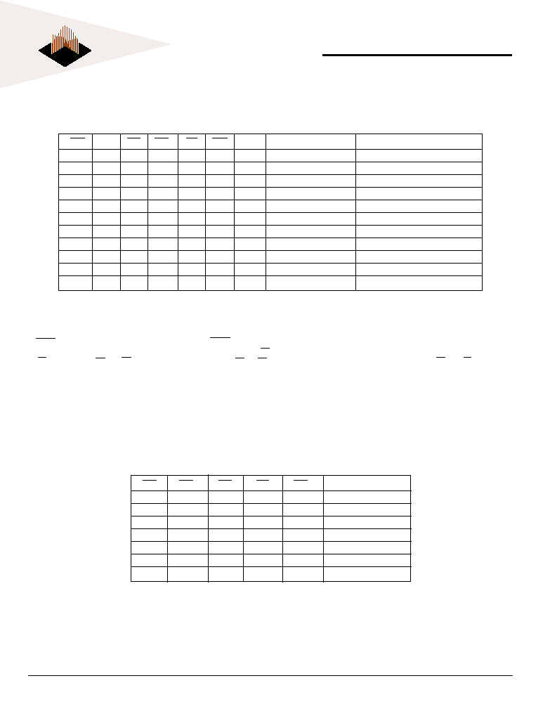
NOTES:
1. X means "Don't Care."
2. The rising edge of clock is symbolized by (
)
3. A continue deselect cycle can only be entered if a deselect cycle is executed first.
4. WRITE = L means Write operation in WRITE TRUTH TABLE. WRITE = H means Read operation in WRITE TRUTH TABLE.
5. Operation finally depends on status of asynchronous input pins (ZZ and OE).
6. CE
X
refers to both CE
A
and CE
B
with the exception that only one CE
A
or CE
B
can be active low at any time. Deselect requires both CE
A
and CE
B
to be high.
CE
CE
CE
CE
CE
X
X
X
X
X
ADV
ADV
ADV
ADV
ADV
WE
WE
WE
WE
WE
BW
BW
BW
BW
BW
X
X
X
X
X
OE
OE
OE
OE
OE
CKE
CKE
CKE
CKE
CKE
CLK
CLK
CLK
CLK
CLK
Address Accessed
Address Accessed
Address Accessed
Address Accessed
Address Accessed
Operation
Operation
Operation
Operation
Operation
H
L
X
X
X
L
N/A
Deselect
X
H
X
X
X
L
N/A
Continue Deselect
L
L
H
X
L
L
External Address
Begin Burst Read Cycle
X
H
X
X
L
L
Next Address
Continue Burst Read Cycle
L
L
H
X
H
L
External Address
NOP/Dummy Read
X
H
X
X
H
L
Next Address
Dummy Read
L
L
L
L
X
L
External Address
Begin Burst Write Cycle
X
H
X
L
X
L
Next Address
Continue Burst Write Cycle
L
L
L
H
X
L
N/A
NOP/Write Abort
X
H
X
H
X
L
Next Address
Write Abort
X
X
X
X
X
H
Current Address
Ignore Clock
TRUTH TABLES
TRUTH TABLES
TRUTH TABLES
TRUTH TABLES
TRUTH TABLES
S
S
S
S
S
YNCHRONOUS
YNCHRONOUS
YNCHRONOUS
YNCHRONOUS
YNCHRONOUS
T
T
T
T
T
RUTH
RUTH
RUTH
RUTH
RUTH
T
T
T
T
T
ABLE
ABLE
ABLE
ABLE
ABLE
W
W
W
W
W
RITE
RITE
RITE
RITE
RITE
T
T
T
T
T
RUTH
RUTH
RUTH
RUTH
RUTH
T
T
T
T
T
ABLE
ABLE
ABLE
ABLE
ABLE
WE
WE
WE
WE
WE
BW
BW
BW
BW
BW
A
A
A
A
A
BW
BW
BW
BW
BW
B
B
B
B
B
BW
BW
BW
BW
BW
C
C
C
C
C
BW
BW
BW
BW
BW
D
D
D
D
D
Operation
Operation
Operation
Operation
Operation
H
X
X
X
X
Read
L
L
H
H
H
Write Byte
A
L
H
L
H
H
Write Byte
B
L
H
H
L
H
Write Byte
C
L
H
H
H
L
Write Byte
D
L
L
L
L
L
Write All Bytes
L
H
H
H
H
Write Abort/NOP
NOTES:
1. X means "Don't Care."
2. All inputs in this table must meet setup and hold time around the rising edge of CLK (
).

4
4
4
4
4
White Electronic Designs Corporation ∑ Westborough, MA ∑ (508) 366-5151
White Electronic Designs
WED2ZL236512S
WED2ZL236512S
WED2ZL236512S
WED2ZL236512S
WED2ZL236512S
A
A
A
A
A
B
B
B
B
B SOL
SOL
SOL
SOL
SOLUTE
UTE
UTE
UTE
UTE
M
M
M
M
M
AXIMUM
AXIMUM
AXIMUM
AXIMUM
AXIMUM
R
R
R
R
R
A
A
A
A
ATINGS
TINGS
TINGS
TINGS
TINGS
*
*
*
*
*
Voltage on V
DD
Supply Relative to V
SS
-0.3V to +3.6V
V
IN
(DQ
X
)
-0.3V to +3.6V
V
IN
(Inputs)
-0.3V to +3.6V
Storage Temperature (BGA)
-55∞C to +125∞C
Short Circuit Output Current
100mA
E
EE
E
E
LECTRIC
LECTRIC
LECTRIC
LECTRIC
LECTRICA L
A L
A L
A L
A L
C
C
C
C
C
HAR
HAR
HAR
HAR
HARA
A
A
A
ACTERISTIC
CTERISTIC
CTERISTIC
CTERISTIC
CTERISTICS
S
S
S
S
(0∞C - T
(0∞C - T
(0∞C - T
(0∞C - T
(0∞C - T
A
A
A
A
A
- 70∞C)
- 70∞C)
- 70∞C)
- 70∞C)
- 70∞C)
*Stress greater than those listed under "Absolute Maximum Ratings: may cause permanent
damage to the device. This is a stress rating only and functional operation of the device at these
or any other conditions greater than those indicated in the operational sections of this
specification is not implied. Exposure to absolute maximum rating condtions for extended
periods may affect reliability.
Description
Description
Description
Description
Description
Symbol
Symbol
Symbol
Symbol
Symbol
Conditions
Conditions
Conditions
Conditions
Conditions
Min
Min
Min
Min
Min
Max
Max
Max
Max
Max
Units
Units
Units
Units
Units
Notes
Notes
Notes
Notes
Notes
Input High (Logic 1) Voltage
V
IH
1.7
VDD +0.3
V
1
Input Low (Logic 0) Voltage
V
IL
-0.3
0.7
V
1
Input Leakage Current
I
LI
0V
£ V
IN
£ V
DD
-5
5
µA
2
Output Leakage Current
I
LO
Output(s) Disabled, 0V
£ V
IN
£ V
DD
-5
5
µA
Output High Voltage
V
OH
I
OH
= -1.0mA
2.0
--
V
1
Output Low Voltage
V
OL
I
OL
= 1.0mA
--
0.4
V
1
Supply Voltage
V
DD
2.375
2.625
V
1
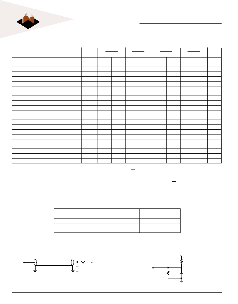
NOTES:
1. All voltages referenced to V
SS
(GND)
2. ZZ pin has an internal pull-up, and input leakage = ± 10µA.
DC C
DC C
DC C
DC C
DC C
HAR
HAR
HAR
HAR
HARA
A
A
A
ACTERISTIC
CTERISTIC
CTERISTIC
CTERISTIC
CTERISTICS
S
S
S
S
NOTES:
1. I
DD
is specified with no output current and increases with faster cycle times. I
DD
increases with faster cycle times and greater output loading.
2. Typical values are measured at 2.5V, 25∞C, and 10ns cycle time.
B
BB
B
BG
G
G
G
GA C
A C
A C
A C
A C
AP
AP
AP
AP
APA
A
A
A
ACIT
CIT
CIT
CIT
CITANCE
ANCE
ANCE
ANCE
ANCE
NOTES:
1. This parameter is sampled.
Description
Description
Description
Description
Description
Symbol
Symbol
Symbol
Symbol
Symbol
Conditions
Conditions
Conditions
Conditions
Conditions
T
T
T
T
Typ
yp
yp
yp
yp
Max
Max
Max
Max
Max
Units
Units
Units
Units
Units
Notes
Notes
Notes
Notes
Notes
Control Input Capacitance
C
I
T
A
= 25∞C; f = 1MHz
3
4
pF
1
Input/Output Capacitance (DQ)
C
O
T
A
= 25∞C; f = 1MHz
4
5
pF
1
Address Capacitance
C
A
T
A
= 25∞C; f = 1MHz
3
5
pF
1
Clock Capacitance
C
CK
T
A
= 25∞C; f = 1MHz
2.5
4
pF
1
166
166
166
166
166
150
150
150
150
150
133
133
133
133
133
100
100
100
100
100
Description
Description
Description
Description
Description
Symbol
Symbol
Symbol
Symbol
Symbol
Conditions
Conditions
Conditions
Conditions
Conditions
T
T
T
T
Typ
yp
yp
yp
yp
MHz
MHz
MHz
MHz
MHz
MHz
MHz
MHz
MHz
MHz
MHz
MHz
MHz
MHz
MHz
MHz
MHz
MHz
MHz
MHz
Units
Units
Units
Units
Units
Notes
Notes
Notes
Notes
Notes
Power Supply
I
DD
Device Selected; All Inputs
£ VIL or ≥ VIH; Cycle
390
360
330
290
mA
1, 2
Current: Operating
Time = t
CYC
MIN; V
DD
= MAX; Output Open
Power Supply
I
SB
2
Device Deselected; V
DD
= MAX; All Inputs
£ V
SS
+ 0.2
30
60
60
60
60
mA
2
Current: Standby
or V
DD
- 0.2; All Inputs Static; CLK Frequency = 0;
ZZ
£ VIL
Power Supply
I
SB
3
Device Selected; All Inputs
£ V
IL
or
≥ V
IH
; Cycle
20
40
40
40
40
mA
2
Current: Current
Time = t
CYC
MIN; V
DD
= MAX; Output Open;
ZZ
≥ VDD - 0.2V
Clock Running
I
SB
4
Device Deselected; V
DD
= MAX; All Inputs
140
120
100
80
mA
2
Standby Current
£ VSS + 0.2 or VDD - 0.2; Cycle Time = t
CYC
MIN; ZZ
£ V
IL
5
5
5
5
5
White Electronic Designs Corporation ∑ (508) 366-5151 ∑ www.whiteedc.com
White Electronic Designs
WED2ZL236512S
WED2ZL236512S
WED2ZL236512S
WED2ZL236512S
WED2ZL236512S
A
A
A
A
AC C
C C
C C
C C
C C
HAR
HAR
HAR
HAR
HARA
A
A
A
ACTERISTIC
CTERISTIC
CTERISTIC
CTERISTIC
CTERISTICS
S
S
S
S
NOTES:
NOTES:
NOTES:
NOTES:
NOTES:
1. All Address inputs must meet the specified setup and hold times for all rising clock (CLK) edges when ADV is sampled low and CEx is sampled low.
All other synchronous inputs must meet the specified setup and hold times whenever this device is chip selected.
2. Chip enable must be valid at each rising edge of CLK (when ADV is Low) to remain enabled.
3. A write cycle is defined by WE low having been registered into the device at ADV Low. A Read cycle is defined by WE High with ADV Low. Both cases
must meet setup and hold times.
O
O
O
O
O
UTPUT
UTPUT
UTPUT
UTPUT
UTPUT
L
L
L
L
L
O
O
O
O
OA D
A D
A D
A D
A D
(A)
(A)
(A)
(A)
(A)
O
O
O
O
O
UTPUT
UTPUT
UTPUT
UTPUT
UTPUT
L
L
L
L
L
O
O
O
O
OA D
A D
A D
A D
A D
(B)
(B)
(B)
(B)
(B)
(FOR
(FOR
(FOR
(FOR
(FOR ttttt
LZC
LZC
LZC
LZC
LZC
,
,
,
,
, ttttt
LZOE
LZOE
LZOE
LZOE
LZOE
,
,
,
,
, ttttt
HZOE
HZOE
HZOE
HZOE
HZOE
, AND
, AND
, AND
, AND
, AND ttttt
HZC
HZC
HZC
HZC
HZC
))
))
)
Symbol
Symbol
Symbol
Symbol
Symbol
166MHz
166MHz
166MHz
166MHz
166MHz
150MHz
150MHz
150MHz
150MHz
150MHz
133MHz
133MHz
133MHz
133MHz
133MHz
100MHz
100MHz
100MHz
100MHz
100MHz
Parameter
Parameter
Parameter
Parameter
Parameter
Min
Min
Min
Min
Min
Max
Max
Max
Max
Max
Min
Min
Min
Min
Min
Max
Max
Max
Max
Max
Min
Min
Min
Min
Min
Max
Max
Max
Max
Max
Min
Min
Min
Min
Min
Max
Max
Max
Max
Max
Units
Units
Units
Units
Units
Clock Time
t
CYC
6.0
6.7
7.5
10.0
ns
Clock Access Time
t
CD
--
3.5
--
3.8
--
4.2
--
5.0
ns
Output enable to Data Valid
t
OE
--
3.5
--
3.8
--
4.2
--
5.0
ns
Clock High to Output Low-Z
t
LZC
1.5
--
1.5
--
1.5
--
1.5
--
ns
Output Hold from Clock High
t
OH
1.5
--
1.5
--
1.5
--
1.5
--
ns
Output Enable Low to output Low-Z
t
LZOE
0.0
--
0.0
--
0.0
--
0.0
--
ns
Output Enable High to Output High-Z
t
HZOE
--
3.0
--
3.0
--
3.5
--
3.5
ns
Clock High to Output High-Z
t
HZC
--
3.0
--
3.0
--
3.5
--
3.5
ns
Clock High Pulse Width
t
CH
2.2
--
2.5
--
3.0
--
3.0
--
ns
Clock Low Pulse Width
t
CL
2.2
--
2.5
--
3.0
--
3.0
--
ns
Address Setup to Clock High
t
AS
1.5
--
1.5
--
1.5
--
1.5
--
ns
CKE Setup to Clock High
t
CES
1.5
--
1.5
--
1.5
--
1.5
--
ns
Data Setup to Clock High
t
DS
1.5
--
1.5
--
1.5
--
1.5
--
ns
Write Setup to Clock High
t
WS
1.5
--
1.5
--
1.5
--
1.5
--
ns
Address Advance to Clock High
t
ADVS
1.5
1.5
1.5
1.5
ns
Chip Select Setup to Clock High
t
CSS
1.5
1.5
1.5
1.5
ns
Address Hold to Clock high
t
AH
0.5
--
0.5
--
0.5
--
0.5
--
ns
CKE Hold to Clock High
t
CEH
0.5
--
0.5
--
0.5
--
0.5
--
ns
Data Hold to Clock High
t
DH
0.5
--
0.5
--
0.5
--
0.5
--
ns
Write Hold to Clock High
t
WH
0.5
--
0.5
--
0.5
--
0.5
--
ns
Address Advance to Clock High
t
ADVH
0.5
--
0.5
--
0.5
--
0.5
--
ns
Chip Select Hold to Clock High
t
CSH
0.5
--
0.5
--
0.5
--
0.5
--
ns
*Including Scope and Jig Capacitance
A
A
A
A
AC T
C T
C T
C T
C T
EST
EST
EST
EST
EST
C
C
C
C
C
ONDITIONS
ONDITIONS
ONDITIONS
ONDITIONS
ONDITIONS
(T
(T
(T
(T
(T
A
A
A
A
A
= 0 TO 70∞C, V
= 0 TO 70∞C, V
= 0 TO 70∞C, V
= 0 TO 70∞C, V
= 0 TO 70∞C, V
DD
DD
DD
DD
DD
= 2.5V ± 5%,
= 2.5V ± 5%,
= 2.5V ± 5%,
= 2.5V ± 5%,
= 2.5V ± 5%, U
U
U
U
U
NLES
NLES
NLES
NLES
NLESS
S
S
S
S
O
O
O
O
O
THERWISE
THERWISE
THERWISE
THERWISE
THERWISE
S
S
S
S
S
PECIFIED
PECIFIED
PECIFIED
PECIFIED
PECIFIED
))
))
)
Parameter
Value
Input Pulse Level
0 to 2.5V
Input Rise and Fall Time (Measured at 20% to 80%)
1.0V/ns
Input and Output Timing Reference Levels
1.25V
Output Load
See Output Load (A)
Dout
Zo=50
RL=50
VL=1.25V
30pF*
Dout
1538
5pF*
+2.5V
1667

6
6
6
6
6
White Electronic Designs Corporation ∑ Westborough, MA ∑ (508) 366-5151
White Electronic Designs
WED2ZL236512S
WED2ZL236512S
WED2ZL236512S
WED2ZL236512S
WED2ZL236512S
SNOOZE MODE
SNOOZE MODE
SNOOZE MODE
SNOOZE MODE
SNOOZE MODE
SNOOZE MODE is a low-current, "power-down" mode in
which the device is deselected and current is reduced to
I
SB
2
Z
. The duration of SNOOZE MODE is dictated by the
length of time Z is in a HIGH state. After the device enters
SNOOZE MODE, all inputs except ZZ become gated in-
puts and are ignored. ZZ is an asynchronous, active HIGH
input that causes the device to enter SNOOZE MODE.
When ZZ becomes a logic HIGH, I
SB
2
Z
is guaranteed after
the setup time tZZ is met. Any READ or WRITE operation
pending when the device enters SNOOZE MODE is not
guaranteed to complete successfully. Therefore, SNOOZE
MODE must not be initiated until valid pending operations
are completed.
S
S
S
S
S
NOOZE
NOOZE
NOOZE
NOOZE
NOOZE
M
M
M
M
M
ODE
ODE
ODE
ODE
ODE
Description
Description
Description
Description
Description
Conditions
Conditions
Conditions
Conditions
Conditions
Symbol
Symbol
Symbol
Symbol
Symbol
Min
Min
Min
Min
Min
Max
Max
Max
Max
Max
Units
Units
Units
Units
Units
Notes
Notes
Notes
Notes
Notes
Current during SNOOZE MODE
ZZ
≥ VIH
I
SB
2
Z
10
mA
ZZ active to input ignored
t
ZZ
2(t
KC
)
ns
1
ZZ inactive to input sampled
t
RZZ
2(t
KC
)
ns
1
ZZ active to snooze current
t
ZZI
2(t
KC
)
ns
1
ZZ inactive to exit snooze current
t
RZZI
ns
1
FIG. 2
FIG. 2
FIG. 2
FIG. 2
FIG. 2 SNOOZE MODE TIMING DIAGRAM
ZZ
I
SUPPLY
CLOCK
ALL INPUTS
(except ZZ)
Output (Q)
t
ZZ
t
ZZI
t
RZZ
t
RZZI
HIGH-Z
DESELECT or READ Only
I
ISB2Z
DON'T CARE

7
7
7
7
7
White Electronic Designs Corporation ∑ (508) 366-5151 ∑ www.whiteedc.com
White Electronic Designs
WED2ZL236512S
WED2ZL236512S
WED2ZL236512S
WED2ZL236512S
WED2ZL236512S
Clock
CKE
Address
WRITE
ADV
OE
Data Out
t
CH
t
CL
t
CES
t
CEH
t
AS
t
AH
A1
A2
A3
t
WS
t
WH
t
CSS
t
CSH
t
OE
t
HZOE
t
LZOE
t
CD
t
OH
t
HZC
Q3-4
Q3-3
Q3-2
Q3-1
Q2-4
Q2-3
Q2-2
Q2-1
Q1-1
Don¢t Care
Undefined
t
CYC
t
ADVS
t
ADVH
CEx
NOTES:
WRITE = L means WE = L, and BWx = L
CEx refers to both CEa and CEb.
A High refers to both CEa and CEb being High.
A Low Refers to either CEa or CEb being Low.
CEa and CEb cannot be Low at the same time.
FIG. 3
FIG. 3
FIG. 3
FIG. 3
FIG. 3 TIMING WAVEFORM OF READ CYCLE
8
8
8
8
8
White Electronic Designs Corporation ∑ Westborough, MA ∑ (508) 366-5151
White Electronic Designs
WED2ZL236512S
WED2ZL236512S
WED2ZL236512S
WED2ZL236512S
WED2ZL236512S
FIG. 4
FIG. 4
FIG. 4
FIG. 4
FIG. 4 TIMING WAVEFORM OF WRITE CYCLE
Clock
Address
WRITE
ADV
Data In
t
CH
t
CL
A2
A3
D2-1
D1-1
D2-2
D2-3
D2-4
D3-1
D3-2
D3-3
OE
Data Out
t
DS
t
DH
Don¢t Care
Undefined
t
CYC
CKE
A1
D3-4
t
CES
t
CEH
Q0-4
t
HZOE
Q0-3
CEx
NOTES: WRITE = L means WE = L, and BWx = L
CEx refers to both CEa and CEb.
A High refers to both CEa and CEb being High.
A Low Refers to either CEa or CEb being Low.
CEa and CEb cannot be Low at the same time.
9
9
9
9
9
White Electronic Designs Corporation ∑ (508) 366-5151 ∑ www.whiteedc.com
White Electronic Designs
WED2ZL236512S
WED2ZL236512S
WED2ZL236512S
WED2ZL236512S
WED2ZL236512S
FIG. 5
FIG. 5
FIG. 5
FIG. 5
FIG. 5 TIMING WAVEFORM OF SINGLE READ/WRITE
Cloc
Address
WRITE
ADV
OE
Data In
t
CH
t
CL
t
DS
t
DH
Data Out
A2
A4
A5
D2
t
OE
t
LZOE
Q1
Don¢t Care
Undefined
t
CYC
CKE
t
CES
t
CEH
A1
A3
A7
A6
Q3
Q4
Q7
Q6
D5
A9
A8
CEx
NOTES:
WRITE = L means WE = L, and BWx = L
CEx refers to both CEa and CEb.
A High refers to both CEa and CEb being High.
A Low Refers to either CEa or CEb being Low.
CEa and CEb cannot be Low at the same time.
k

1 0
1 0
1 0
1 0
1 0
White Electronic Designs Corporation ∑ Westborough, MA ∑ (508) 366-5151
White Electronic Designs
WED2ZL236512S
WED2ZL236512S
WED2ZL236512S
WED2ZL236512S
WED2ZL236512S
FIG. 6
FIG. 6
FIG. 6
FIG. 6
FIG. 6 TIMING WAVEFORM OF CKE OPERATION
Clock
Address
WRITE
ADV
OE
Data In
t
CH
t
CL
Data Out
A1
A2
A3
A4
A5
t
CES
t
CEH
Don¢t Care
Undefined
t
CYC
CKE
t
DS
t
DH
D2
Q4
Q1
t
CD
t
LZC
t
HZC
Q3
A6
CEx
NOTES:
WRITE = L means WE = L, and BWx = L
CEx refers to both CEa and CEb.
A High refers to both CEa and CEb being High.
A Low Refers to either CEa or CEb being Low.
CEa and CEb cannot be Low at the same time.
1 1
1 1
1 1
1 1
1 1
White Electronic Designs Corporation ∑ (508) 366-5151 ∑ www.whiteedc.com
White Electronic Designs
WED2ZL236512S
WED2ZL236512S
WED2ZL236512S
WED2ZL236512S
WED2ZL236512S
Clock
Address
WRITE
ADV
OE
Data In
t
CH
t
CL
Data Out
A1
A2
A3
A4
A5
Don¢t Care
Undefined
t
CYC
CKE
D5
Q4
t
CES
t
CEH
Q1
Q2
t
OE
t
LZOE
D3
t
CD
t
LZC
t
HZC
t
DH
t
DS
CEx
NOTES:
WRITE = L means WE = L, and BWx = L
CEx refers to both CEa and CEb.
A High refers to both CEa and CEb being High.
A Low Refers to either CEa or CEb being Low.
CEa and CEb cannot be Low at the same time.
FIG. 7
FIG. 7
FIG. 7
FIG. 7
FIG. 7 TIMING WAVEFORM OF CE OPERATION
1 2
1 2
1 2
1 2
1 2
White Electronic Designs Corporation ∑ Westborough, MA ∑ (508) 366-5151
White Electronic Designs
WED2ZL236512S
WED2ZL236512S
WED2ZL236512S
WED2ZL236512S
WED2ZL236512S
Commercial T
Commercial T
Commercial T
Commercial T
Commercial Temp Range (0∞C to 70∞C)
emp Range (0∞C to 70∞C)
emp Range (0∞C to 70∞C)
emp Range (0∞C to 70∞C)
emp Range (0∞C to 70∞C)
P
P
P
P
Par
ar
ar
ar
art Number
t Number
t Number
t Number
t Number
Configuration
Configuration
Configuration
Configuration
Configuration
tCD
tCD
tCD
tCD
tCD
Clock
Clock
Clock
Clock
Clock
(ns)
(ns)
(ns)
(ns)
(ns)
(MHz)
(MHz)
(MHz)
(MHz)
(MHz)
WED2ZL236512S35BC
2 x 512K x 36
3.5
166
WED2ZL236512S38BC
2 x 512K x 36
3.8
150
WED2ZL236512S42BC
2 x 512K x 36
4.2
133
WED2ZL236512S50BC
2 x 512K x 36
5.0
100
P
PP
P
PA
A
A
A
ACK
CK
CK
CK
CKA
A
A
A
AGE DIMENSION:
GE DIMENSION:
GE DIMENSION:
GE DIMENSION:
GE DIMENSION: 119 BUMP PBGA
ALL LINEAR DIMENSIONS ARE IN MILLIMETERS AND PARENTHETICALLY IN INCHES
2.79 (0.110)
MAX
0.711 (0.028)
MAX
1.27 (0.050)
TYP
1.27 (0.050) TYP
A
B
C
D
E
F
G
H
J
K
L
M
N
P
R
T
U
17.00 (0.669) TYP
A1
CORNER
32 (0.800)
TYP
23.00 (0.905)
TYP
7.62 (0.300)
TYP
R 1.52 (0.060)
MAX (4x)
ORDERING INFORMA
ORDERING INFORMA
ORDERING INFORMA
ORDERING INFORMA
ORDERING INFORMATION
TION
TION
TION
TION