1
White Electronic Designs Corporation (508) 366-5151 www.whiteedc.com
WED2ZL361MS
White Electronic Designs
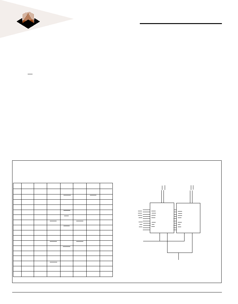
DESCRIPTION
The WEDC SyncBurst - SRAM family employs high-
speed, low-power CMOS designs that are fabricated
using an advanced CMOS process. WEDCs 32Mb
SyncBurst SRAMs integrate two 1M x 18 SRAMs into a
single BGA package to provide 1M x 36 configuration. All
synchronous inputs pass through registers controlled
by a positive-edge-triggered single-clock input (CLK).
The NBL or No Bus Latency Memory utilizes all the band-
width in any combination of operating cycles. Address,
data inputs, and all control signals except output en-
able and linear burst order are synchronized to input
clock. Burst order control must be tied High or Low.
Asynchronous inputs include the sleep mode enable
(ZZ). Output Enable controls the outputs at any given
time. Write cycles are internally self-timed and initiated
by the rising edge of the clock input. This feature elimi-
nates complex off-chip write pulse generation and pro-
vides increased timing flexibility for incoming signals.
NOTE: NBL (No Bus Latency) is equivalent to ZBT
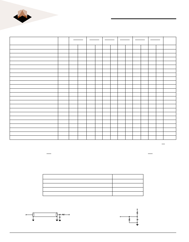
1Mx36 Synchronous Pipeline Burst NBL SRAM
FIG. 1
B
LOCK
D
IAGRAM
P
IN
C
ONFIGURATION
(TOP VIEW)
Address Bus
(SA
0
-
SA
19
)
DQa, DQb
DQPa, DQPb
DQc, DQd
DQPc, DQPd
DQa
-
DQd
DQPa
-
DQPd
1M x 18
1M x 18
CLK
CKE
ADV
LBO
CS1
CS2
CS2
OE
WE
ZZ
CLK
CKE
ADV
LBO
CE1
CE2
CE2
OE
WE
ZZ
CLK
CKE
ADV
LBO
CS1
CS2
CS2
OE
WE
ZZ
BWd
BWa
BWc
BWb
FEATURES
n Fast clock speed: 250, 225, 200, 166, 150, 133MHz
n Fast access times: 2.6, 2.8, 3.0, 3.5, 3.8, 4.2ns
n Fast OE access times: 2.6, 2.8, 3.0, 3.5, 3.8, 4.2ns
n Separate +2.5V � 5% power supplies for Core, I/O
(V
DD
, V
DDQ
)
n Snooze Mode for reduced-standby power
n Individual Byte Write control
n Clock-controlled and registered addresses, data
I/Os and control signals
n Burst control (interleaved or linear burst)
n Packaging:
119-bump BGA package
n Low capacitive bus loading
1
2
3
4
5
6
7
A
V
DDQ
SA
SA
SA
SA
SA
V
DDQ
B
SA
CE2
SA
ADV
SA
CE2
NC
C
NC
SA
SA
V
DD
SA
SA
NC
D
DQ
c
DQP
c
V
SS
NC
V
SS
DQP
b
DQ
b
E
DQ
c
DQ
c
V
SS
CE1
V
SS
DQ
b
DQ
b
F
V
DDQ
DQ
c
V
SS
OE
V
SS
DQ
b
V
DDQ
G
DQ
c
DQ
c
BW
c
SA
BW
b
DQ
b
DQ
b
H
DQ
c
DQ
c
V
SS
WE
V
SS
DQ
b
DQ
b
J
V
DDQ
V
DD
NC
V
DD
NC
V
DD
V
DDQ
K
DQ
d
DQ
d
V
SS
CLK
V
SS
DQ
a
DQ
a
L
DQ
d
DQ
d
BW
d
NC
BW
a
DQ
a
DQ
a
M
V
DDQ
DQ
d
V
SS
CKE
V
SS
DQ
a
V
DDQ
N
DQ
d
DQ
d
V
SS
SA1
V
SS
DQ
a
DQ
a
P
DQ
d
DQP
d
V
SS
SA0
V
SS
DQP
a
DQ
a
R
NC
SA
LBO
V
DD
NC
SA
NC
T
N C
N C
SA
SA
SA
N C
Z Z
U
V
DDQ
NC
NC
NC
NC
NC
V
DDQ
October 2002 Rev. 5
ECO # 15466
2
White Electronic Designs Corporation Westborough MA (508) 366-5151
WED2ZL361MS
White Electronic Designs
FUNCTION DESCRIPTION
The WED2ZL361MS is an NBL SSRAM designed to sus-
tain 100% bus bandwidth by eliminating turnaround
cycle when there is transition from Read to Write, or vice
versa. All inputs (with the exception of OE, LBO and ZZ)
are synchronized to rising clock edges.
All read, write and deselect cycles are initiated by the
ADV input. Subsequent burst addresses can be inter-
nally generated by the burst advance pin (ADV). ADV
should be driven to Low once the device has been dese-
lected in order to load a new address for next operation.
Clock Enable (CKE) pin allows the operation of the chip
to be suspended as long as necessary. When CKE is
high, all synchronous inputs are ignored and the inter-
nal device registers will hold their previous values. NBL
SSRAM latches external address and initiates a cycle
when CKE and ADV are driven low at the rising edge of
the clock.
Output Enable (OE) can be used to disable the output at
any given time. Read operation is initiated when at the
rising edge of the clock, the address presented to the
address inputs are latched in the address register, CKE
is driven low, the write enable input signals WE are
driven high, and ADV driven low. The internal array is
read between the first rising edge and the second ris-
ing edge of the clock and the data is latched in the out-
put register. At the second clock edge the data is driven
out of the SRAM. During read operation OE must be
driven low for the device to drive out the requested data.
B
URST
S
EQUENCE
T
ABLE
NOTE 1: LBO pin must be tied to High or Low, and Floating State
must not be allowed.
Write operation occurs when WE is driven low at the
rising edge of the clock. BW[d:a] can be used for byte
write operation. The pipe-lined NBL SSRAM uses a
late-late write cycle to utilize 100% of the bandwidth. At
the first rising edge of the clock, WE and address are
registered, and the data associated with that address
is required two cycle later.
Subsequent addresses are generated by ADV High for
the burst access as shown below. The starting point of
the burst seguence is provided by the external address.
The burst address counter wraps around to its initial
state upon completion. The burst sequence is deter-
mined by the state of the LBO pin. When this pin is low,
linear burst sequence is selected. And when this pin is
high, Interleaved burst sequence is selected.
During normal operation, ZZ must be driven low. When
ZZ is driven high, the SRAM will enter a Power Sleep
Mode after 2 cycles. At this time, internal state of the
SRAM is preserved. When ZZ returns to low, the SRAM
operates after 2 cycles of wake up time.
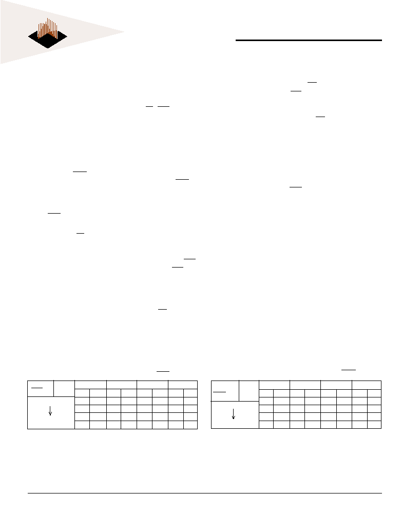
(Interleaved Burst, LBO = High)
Case 1 Case 2 Case 3 Case 4
A1
A0
A1
A0
A1
A0
A1
A0
0
0
0
1
1
0
1
1
0
1
0
0
1
1
1
0
1
0
1
1
0
0
0
1
1
1
1
0
0
1
0
0
LBO Pin High
First Address
Fourth Address
Case 1 Case 2 Case 3 Case 4
A1
A0
A1
A0
A1
A0
A1
A0
0
0
0
1
1
0
1
1
0
1
1
0
1
1
0
0
1
0
1
1
0
0
0
1
1
1
0
0
0
1
1
0
LBO Pin High
First Address
Fourth Address
(Linear Burst, LBO = Low)
3
White Electronic Designs Corporation (508) 366-5151 www.whiteedc.com
WED2ZL361MS
White Electronic Designs
TRUTH TABLES
S
YNCHRONOUS
T
RUTH
T
ABLE
W
RITE
T
RUTH
T
ABLE
CEx
ADV WE
BWx
OE
CKE CLK
Address Accessed
Operation
H
L
X
X
X
L
N/A
Deselect
X
H
X
X
X
L
N/A
Continue Deselect
L
L
H
X
L
L
External Address
Begin Burst Read Cycle
X
H
X
X
L
L
Next Address
Continue Burst Read Cycle
L
L
H
X
H
L
External Address
NOP/Dummy Read
X
H
X
X
H
L
Next Address
Dummy Read
L
L
L
L
X
L
External Address
Begin Burst Write Cycle
X
H
X
L
X
L
Next Address
Continue Burst Write Cycle
L
L
L
H
X
L
N/A
NOP/Write Abort
X
H
X
H
X
L
Next Address
Write Abort
X
X
X
X
X
H
Current Address
Ignore Clock
NOTES:
1. X means Dont Care.
2. The rising edge of clock is symbolized by ( )
3. A continue deselect cycle can only be entered if a deselect cycle is executed first.
4. WRITE = L means Write operation in WRITE TRUTH TABLE.
WRITE = H means Read operation in WRITE TRUTH TABLE.
5. Operation finally depends on status of asynchronous input pins (ZZ and OE).
6. CEx refers to the combination of CE
1
, CE
2
and CE
2
.
WE
BWa
BWb
BWc
BWd
Operation
H
X
X
X
X
Read
L
L
H
H
H
Write Byte a
L
H
L
H
H
Write Byte b
L
H
H
L
H
Write Byte c
L
H
H
H
L
Write Byte d
L
L
L
L
L
Write All Bytes
L
H
H
H
H
Write Abort/NOP
NOTES:
1. X means Dont Care.
2. All inputs in this table must meet setup and hold time around the rising edge of
CLK ( ).
4
White Electronic Designs Corporation Westborough MA (508) 366-5151
WED2ZL361MS
White Electronic Designs
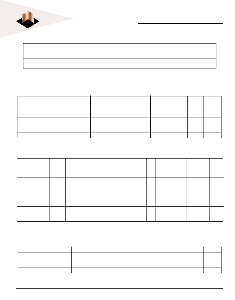
A
BSOLUTE
M
AXIMUM
R
ATINGS
*
R
ECOMMENDED
DC O
PERATING
C
ONDITIONS
(V
OLTAGE
R
EFERENCED
TO
: V
SS
= OV, T
A
= 0�C; C
OMMERCIAL
OR
T
A
= -40�C
TO
+85�C; I
NDUSTRIAL
)
*Stress greater than those listed under Absolute Maximum Ratings: may cause permanent damage to the device. This is a stress
rating only and functional operation of the device at these or any other conditions greater than those indicated in the operational
sections of this specification is not implied. Exposure to absolute maximum rating condtions for extended periods may affect reliability.
NOTES:
1. All voltages referenced to VSS (GND)
2. ZZ pin has an internal pull-up, and input leakage is higher.
DC C
HARACTERISTICS
NOTES:
1. I
DD
is specified with no output current and increases with faster cycle times.
I
DD
increases with faster cycle times and greater output loading.
2. Typical values are measured at 2.5V, 25�C, and 10ns cycle time.
BGA C
APACITANCE
NOTES:
1. This parameter is sampled.
Description
SymbolConditions
Typ
Max
Units
Notes
Control Input Capacitance
C
I
T
A
= 25�C; f = 1MHz
5
7
pF
1
Input/Output Capacitance (DQ)
C
O
T
A
= 25�C; f = 1MHz
6
8
pF
1
Address Capacitance
C
A
T
A
= 25�C; f = 1MHz
5
7
pF
1
Clock Capacitance
C
CK
T
A
= 25�C; f = 1MHz
3
5
pF
1
250
200
166
133
Description
Symbol
Conditions
Typ
MHz MHz MHz MHz
Units Notes
Power Supply
I
DD
Device Selected; All Inputs
�
V
IL
or
�
V
IH
; Cycle
900
800
690
580
mA
1, 2
Current: Operating
Time = T
CYC
MIN; V
DD
= MAX; Output Open
Power Supply
I
SB
2
Device Deselected; V
DD
= MAX; All Inputs
�
V
SS
+ 0.2
30
60
60
60
60
mA
2
Current: Standby
or V
DD
- 0.2; All Inputs Static; CLK Frequency = 0;
ZZ
�
V
IL
Power Supply
I
SB
3
Device Selected; All Inputs
�
V
IL
or
�
V
IH
; Cycle
20
40
40
40
40
mA
2
Current: Current
Time = T
CYC
MIN; V
DD
= MAX; Output Open;
ZZ
�
V
DD
- 0.2V
Clock Running
I
SB
4
Device Deselected; V
DD
= MAX; All Inputs
150
140
130
100
mA
2
Standby Current
�
V
SS
+ 0.2 or V
DD
- 0.2; Cycle Time = T
CYC
MIN; ZZ
�
V
IL
Voltage on V
DD
Supply Relative to V
SS
-0.3V to +3.6V
V
IN
(DQx)
-0.3V to +3.6V
V
IN
(Inputs)
-0.3V to +3.6V
Storage Temperature (BGA)
-55�C to +125�C
Short Circuit Output Current
100mA
Description
SymbolConditions
Min
Max
Units
Notes
Input High (Logic 1) Voltage
V
IH
1.7
V
DD
+0.3
V
1
Input Low (Logic 0) Voltage
V
IL
-0.3
0.7
V
1
Input Leakage Current
I
LI
0V � V
IN
� V
DD
-5
5
�A
2
Output Leakage Current
I
LO
Output(s) Disabled, 0V � V
IN
� V
DD
-5
5
�A
Output High Voltage
V
OH
I
OH
= -1.0mA
2.0
V
1
Output Low Voltage
V
OL
I
OL
= 1.0mA
0.4
V
1
Supply Voltage
V
DD
2.375
2.625
V
1
5
White Electronic Designs Corporation (508) 366-5151 www.whiteedc.com
WED2ZL361MS
White Electronic Designs
AC C
HARACTERISTICS
NOTES:
1. All Address inputs must meet the specified setup and hold times for all rising clock (CLK) edges when ADV is sampled low and CEx is
sampled valid. All other synchronous inputs must meet the specified setup and hold times whenever this device is chip selected.
2. Chip enable must be valid at each rising edge of CLK (when ADV is Low) to remain enabled.
3. A write cycle is defined by WE low having been registered into the device at ADV Low. A Read cycle is defined by WE High with ADV Low.
Both cases must meet setup and hold times.
O
UTPUT
L
OAD
(A)
O
UTPUT
L
OAD
(B)
(
FOR
t
LZC
, t
LZOE
, t
HZOE
,
AND
t
HZC
)
Dout
Zo=50
RL=50
VL=1.25V
30pF*
Dout
1538
5pF*
+2.5V
1667
*Including Scope and Jig Capacitance
AC T
EST
C
ONDITIONS
(T
A
= 0
TO
70�C, V
DD
= 2.5V � 5%; C
OMMERCIAL
OR
T
A
= -40�C
TO
+85�C; V
DD
= 2.5V � 5%; I
NDUSTRIAL
)
Parameter
Value
Input Pulse Level
0 to 2.5V
Input Rise and Fall Time (Measured at 20% to 80%)
1.0V/ns
Input and Output Timing Reference Levels
1.25V
Output Load
See Output Load (A)
Symbol
250MHz
225MHz
200MHz
166MHz
150MHz
133MHz
Parameter
Min
Max
Min Max Min Max Min Max Min Max Min Max
Units
Clock Time
t
C Y C
4.0
4.4
5.0
6.0
6.7
7.5
ns
Clock Access Time
t
CD
--
2.6
--
2.8
--
3.0
--
3.5
--
3.8
--
4.2
ns
Output enable to Data Valid
t
OE
--
2.6
--
2.8
--
3.0
--
3.5
--
3.8
--
4.2
ns
Clock High to Output Low-Z
t
LZC
1.5
--
1.5
--
1.5
--
1.5
--
1.5
--
1.5
--
ns
Output Hold from Clock High
t
OH
1.5
--
1.5
--
1.5
--
1.5
--
1.5
--
1.5
--
ns
Output Enable Low to output Low-Z
t
LZOE
0.0
--
0.0
--
0.0
--
0.0
--
0.0
--
0.0
--
ns
Output Enable High to Output High-Z
t
HZOE
--
2.6
--
2.8
--
3.0
--
3.0
--
3.0
--
3.5
ns
Clock High to Output High-Z
t
HZC
--
2.6
--
2.8
--
3.0
--
3.0
--
3.0
--
3.5
ns
Clock High Pulse Width
t
CH
1.7
--
2.0
--
2.0
--
2.2
--
2.2
--
2.2
--
ns
Clock Low Pulse Width
t
CL
1.7
--
2.0
--
2.0
--
2.2
--
2.2
--
2.2
--
ns
Address Setup to Clock High
t
A S
1.2
--
1.4
--
1.4
--
1.5
--
1.5
--
1.5
--
ns
CKE Setup to Clock High
t
C E S
1.2
--
1.4
--
1.4
--
1.5
--
1.5
--
1.5
--
ns
Data Setup to Clock High
t
DS
1.2
--
1.4
--
1.4
--
1.5
--
1.5
--
1.5
--
ns
Write Setup to Clock High
t
WS
1.2
--
1.4
--
1.4
--
1.5
--
1.5
--
1.5
--
ns
Address Advance to Clock High
t
A D V S
1.2
--
1.4
--
1.4
--
1.5
--
1.5
--
1.5
--
ns
Chip Select Setup to Clock High
t
C S S
1.2
--
1.4
--
1.4
--
1.5
--
1.5
--
1.5
--
ns
Address Hold to Clock high
t
AH
0.3
--
0.4
--
0.4
--
0.5
--
0.5
--
0.5
--
ns
CKE Hold to Clock High
t
CEH
0.3
--
0.4
--
0.4
--
0.5
--
0.5
--
0.5
--
ns
Data Hold to Clock High
t
DH
0.3
--
0.4
--
0.4
--
0.5
--
0.5
--
0.5
--
ns
Write Hold to Clock High
t
WH
0.3
--
0.4
--
0.4
--
0.5
--
0.5
--
0.5
--
ns
Address Advance to Clock High
t
ADVH
0.3
--
0.4
--
0.4
--
0.5
--
0.5
--
0.5
--
ns
Chip Select Hold to Clock High
t
CSH
0.3
--
0.4
--
0.4
--
0.5
--
0.5
--
0.5
--
ns
ZZ High to Power Down
t
P D S
2
--
2
--
2
--
2
--
2
--
2
--
cycle
ZZ Low to Power Up
t
P U S
2
--
2
--
2
--
2
--
2
--
2
--
cycle