
WED2ZL64512S
October 2001
Rev. 0
1
White Electronic Designs Corporation ∑ (602) 437-1520 ∑ www.wedc.com
White Electronic Designs
White Electronic Designs Corp. reserves the right to change products or specifications without notice.
DESCRIPTION
The WEDC SyncBurst - SRAM family employs high-
speed, low-power CMOS designs that are fabricated
using an advanced CMOS process. WEDC's 32Mb Sync
SRAM integrate two 512K x 32 SRAMs into a single
BGA package to provide 512K x 64 configuration. All
synchronous inputs pass through registers controlled by
a positive-edge-triggered single-clock input (CK). The
NBL or No Bus Latency Memory utilizes all the bandwidth
in any combination of operating cycles. Address, data
inputs, and all control signals except output enable are
synchronized to input clock. Output Enable controls the
outputs at any given time and to Asynchronous Input.
Write cycles are internally self-timed and initiated by the
rising edge of the clock input. This feature eliminates
complex off-chip write pulse generation and provides
increased timing flexibility for incoming signals.
NOTE: NBL = No Bus Latency is equivalent to the industry ZBTTM devices.
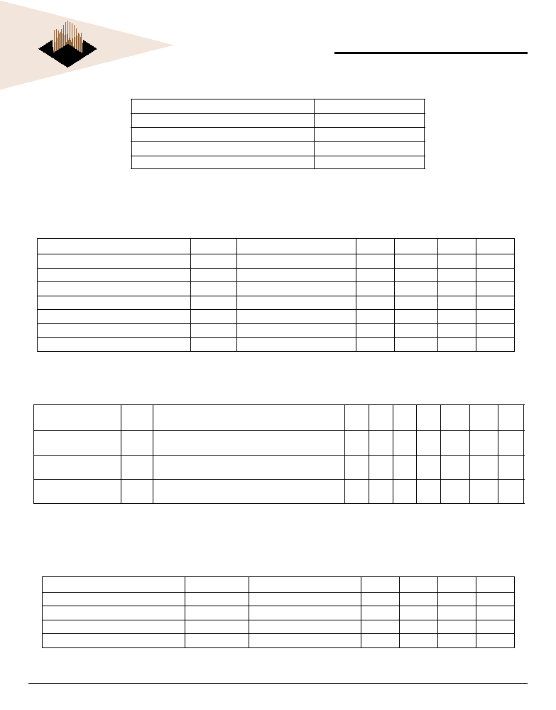
512K x 64 Synchronous Pipeline NBL SRAM
BLOCK DIAGRAM
FIG. 1
PIN CONFIGURATION
(TOP VIEW)
SA
0
≠
18
512K x 36
512K x 36
DQ
0
≠
31
DQ
32
≠
63
OE
B
WEB_LW
CK
CS
2B
CS
2
CS
1B
OE#
WE#
CK
CS
2
#
CS
2
CS
1
#
OE#
WE#
CK
CS
2
#
CS
2
CS
1
#
DQ
0
≠
31
A
0
≠ A
18
A
0
≠ A
18
DQ
0
≠
31
WEB_HW
U1
U2
FEATURES
Fast clock speed: 166, 150, 133, and 100MHz
Fast access times: 3.5ns, 3.8ns, 4.2ns, and 5.0ns
Fast OE# access times: 3.5ns, 3.8ns, 4.2ns, and
5.0ns
Seperate +2.5V ± 5% power supplys for core I/O
(V
CC
+ V
CCQ
)
Double Word Write Control
Clock-controlled and registered addresses, data I/Os
and control signals
Packaging:
∑ 119 bump BGA package
Low capacitive bus loading
1
2
3
4
5
6
7
8
9
A
DQ
F
DQ
F
DQ
F
DQ
F
NC
DQ
G
DQ
G
DQ
G
DQ
G
B
DQ
F
DQ
F
DQ
F
DQ
F
NC
DQ
G
DQ
G
DQ
G
DQ
G
C
DQ
E
DQ
E
DQ
E
DQ
E
NC
DQ
H
DQ
H
DQ
H
DQ
H
D
DQ
E
DQ
E
DQ
E
DQ
E
NC
DQ
H
DQ
H
DQ
H
DQ
H
E
NC
NC
NC V
CCQ
V
CCQ
V
CCQ
NC
NC
NC
F
SA
V
CCQ
V
CC
V
CC
V
CC
V
CC
V
CC
V
CCQ
SA
G
SA
CE#
V
SS
V
SS
V
SS
V
SS
V
SS
SA
SA
H
SA
NC
V
SS
WE
1
# V
SS
V
SS
V
SS
SA
SA
J
SA
18
CE
2
# SS
CK
OE#
NC
NC
NC
SA
1
SA
0
K
SA
CE
2
V
SS
WE
0
# V
SS
V
SS
V
SS
SA
SA
L
SA
NC
V
SS
V
SS
V
SS
V
SS
V
SS
SA
SA
M
SA
V
CCQ
V
CC
V
CC
V
CC
V
CC
V
CC
V
CCQ
SA
N
NC
NC
NC V
CCQ
V
CCQ
V
CCQ
NC
NC
NC
P
DQ
D
DQ
D
DQ
D
DQ
D
NC
DQ
A
DQ
A
DQ
A
DQ
A
R
DQ
D
DQ
D
DQ
D
DQ
D
NC
DQ
A
DQ
A
DQ
A
DQ
A
T
DQ
C
DQ
C
DQ
C
DQ
C
NC
DQ
B
DQ
B
DQ
B
DQ
B
U
DQ
C
DQ
C
DQ
C
DQ
C
NC
DQ
B
DQ
B
DQ
B
DQ
B

WED2ZL64512S
October 2001
Rev. 0
2
White Electronic Designs Corporation ∑ (602) 437-1520 ∑ www.wedc.com
White Electronic Designs
White Electronic Designs Corp. reserves the right to change products or specifications without notice.
rising edge and the second rising edge of the clock and
the data is latched in the output register. At the second
clock edge the data is driven out of the SRAM. During
read operation OE# must be driven low for the device to
drive out the requested data.
Write operation occurs when WE# is driven low at the
rising edge of the clock. The pipe-lined NBL SSRAM uses
a late-late write cycle to utilize 100% of the bandwidth. At
the first rising edge of the clock, WE# and address are
registered, and the data associated with that address is
required two cycle later.
TRUTH TABLES
SYNCHRONOUS TRUTH TABLE
FUNCTION DESCRIPTION
The WED2ZL64512S is an NBL SSRAM designed to
sustain 100% bus bandwidth by eliminating turnaround
cycle when there is transition from Read to Write, or
vice versa. All inputs (with the exception of OE#) are
synchronized to rising clock edges.
Output Enable (OE#) can be used to disable the output
at any given time. Read operation is initiated when at
the rising edge of the clock, the address presented to
the address inputs are latched in the address register,
CKE# is driven low, the write enable input signals WE#
are driven high. The internal array is read between the first
CEx#
WE#
OE#
CK
Address Accessed
Operation
H
X
X
N/A
Deselect
L
H
L
Current Address
Read Cycle
L
H
H
N/A
NOP/Dummy Read
X
X
H
N/A
Dummy Read
L
L
X
Current Address
Write Cycle
L
L
X
N/A
NOP/Write Abort
NOTES:
1. X means "Don't Care."
2. The rising edge of clock is symbolized by ( )
3. A continue deselect cycle can only be entered if a deselect cycle is executed first.
4. WRITE# = L means Write operation in WRITE TRUTH TABLE.
WRITE# = H means Read operation in WRITE TRUTH TABLE.
WED2ZL64512S
October 2001
Rev. 0
3
White Electronic Designs Corporation ∑ (602) 437-1520 ∑ www.wedc.com
White Electronic Designs
White Electronic Designs Corp. reserves the right to change products or specifications without notice.
ABSOLUTE MAXIMUM RATINGS*
Voltage on V
CC
Supply Relative to Vss
-0.3V T
A
+3.6V
V
IN
(DQx)
-0.3V T
A
+3.6V
V
IN
(Inputs)
-0.3V T
A
+3.6V
Storage Temperature (BGA)
-55∞C T
A
+125∞C
Short Circuit Output Current
100mA
*Stress greater than those listed under "Absolute Maximum Ratings: may cause permanent damage to the device. This is a stress rating
only and functional operation of the device at these or any other conditions greater than those indicated in the operational sections of this
specification is not implied. Exposure to absolute maximum rating condtions for extended periods may affect reliability.
ELECTRICAL CHARACTERISTICS (0∞C T
A
70∞C)
Description
Symbol
Conditions
Min
Max
Units
Notes
Input High (Logic 1) Voltage
V
IH
1.7
V
CC
+0.3
V
1
Input Low (Logic 0) Voltage
V
IL
-0.3
0.7
V
1
Input Leakage Current
I
LI
0V V
IN
V
CC
-5
5
mA
Output Leakage Current
I
LO
Output(s) Disabled, 0V V
IN
V
CC
-5
5
mA
Output High Voltage
V
OH
I
OH
= -1.0mA
2.0
---
V
1
Output Low Voltage
V
OL
I
OL
= 1.0mA
---
0.4
V
1
Supply Voltage
V
CC
2.375
2.625
V
1
NOTES:
1. All voltages referenced to V
SS
(GND)
BGA CAPACITANCE
NOTES:
1. This parameter is sampled.
Description
Symbol
Conditions
Typ
Max
Units
Notes
Control Input Capacitance
C
L
T
A
= 25∞C; f = 1MHz
5
7
pF
1
Input/Output Capacitance (DQ)
C
O
T
A
= 25∞C; f = 1MHz
6
8
pF
1
Address Capacitance
C
A
T
A
= 25∞C; f = 1MHz
5
7
pF
1
Clock Capacitance
C
CK
T
A
= 25∞C; f = 1MHz
3
5
pF
1
DC CHARACTERISTICS
NOTES:
1. I
CC
is specified with no output current and increases with faster cycle times. I
CC
increases with faster cycle times and greater output loading.
2. Typical values are measured at 2.5V, 25∞C, and 10ns cycle time.
Description
Symbol
Conditions
Typ
166
MH
Z
150
MH
Z
133
MH
Z
100
MH
Z
Units Notes
Power Supply
Current: Operating
I
CC
Device Selected; All Inputs V
IL
or V
IH
; Cycle
Time = T
CYC
MIN; V
CC
= MAX; Output Open
650
600
560
500
mA
1, 2
Power Supply
Current: Standby
I
SB2
Device Deselected; V
CC
= MAX; All Inputs V
SS
+ 0.2
or V
CC
- 0.2; All Inputs Static; CK Frequency = 0
30
60
60
60
60
mA
2
Clock Running
Standby Current
I
SB4
Device Deselected; V
CC
= MAX; All Inputs
V
SS
+ 0.2 or V
CC
- 0.2; Cycle Time = T
CYC
MIN
140
120
100
80
mA
2

WED2ZL64512S
October 2001
Rev. 0
4
White Electronic Designs Corporation ∑ (602) 437-1520 ∑ www.wedc.com
White Electronic Designs
White Electronic Designs Corp. reserves the right to change products or specifications without notice.
Parameter
Symbol
166MHz
150MHz
133MHz
100MHz
Units
Min
Max
Min
Max
Min
Max
Min
Max
Clock Time
t
CYC
6.0
6.7
7.5
10.0
ns
Clock Access Time
t
CD
--
3.5
--
3.8
--
4.2
--
5.0
ns
Output enable to Data Valid
t
OE
--
3.5
--
3.8
--
4.2
--
5.0
ns
Clock High to Output Low-Z
t
LZC
1.5
--
1.5
--
1.5
--
1.5
--
ns
Output Hold from Clock High
t
OH
1.5
--
1.5
--
1.5
--
1.5
--
ns
Output Enable Low to output Low-Z
t
LZOE
0.0
--
0.0
--
0.0
--
0.0
--
ns
Output Enable High to Output High-Z
t
HZOE
--
3.0
--
3.0
--
3.5
--
3.5
ns
Clock High to Output High-Z
t
HZC
--
3.0
--
3.0
--
3.5
--
3.5
ns
Clock High Pulse Width
t
CH
2.2
--
2.5
--
3.0
--
3.0
--
ns
Clock Low Pulse Width
t
CL
2.2
--
2.5
--
3.0
--
3.0
--
ns
Address Setup to Clock High
t
AS
1.5
--
1.5
--
1.5
--
1.5
--
ns
CKE Setup to Clock High
t
CES
1.5
--
1.5
--
1.5
--
1.5
--
ns
Data Setup to Clock High
t
DS
1.5
--
1.5
--
1.5
--
1.5
--
ns
Write Setup to Clock High
t
WS
1.5
--
1.5
--
1.5
--
1.5
--
ns
Chip Select Setup to Clock High
t
CSS
1.5
1.5
1.5
1.5
ns
Address Hold to Clock high
t
AH
0.5
--
0.5
--
0.5
--
0.5
--
ns
CKE Hold to Clock High
t
CEH
0.5
--
0.5
--
0.5
--
0.5
--
ns
Data Hold to Clock High
t
DH
0.5
--
0.5
--
0.5
--
0.5
--
ns
Write Hold to Clock High
t
WH
0.5
--
0.5
--
0.5
--
0.5
--
ns
Chip Select Hold to Clock High
t
CSH
0.5
--
0.5
--
0.5
--
0.5
--
ns
AC CHARACTERISTICS
NOTES:
1. All Address inputs must meet the specified setup and hold times for all rising clock (CK) edges when ADV is sampled low and CE
X
# is sampled valid.
All other synchronous inputs must meet the specified setup and hold times whenever this device is chip selected.
2. Chip enable must be valid at each rising edge of CK (when ADV is Low) to remain enabled.
3. A write cycle is defined by WE# low having been registered into the device. A Read cycle is defined by WE# High.
Both cases must meet setup and hold times.
OUTPUT LOAD (A)
OUTPUT LOAD (B)
(
FOR
t
LZC
, t
LZOE
, t
HZOE
, and t
HZC
)
D
OUT
Zo=50
RL=50
VL=1.25V
30pF*
D
OUT
1538
5pF*
+2.5V
1667
*Including Scope and Jig Capacitance
AC TEST CONDITIONS
(0∞C T
A
70∞C, V
CC
= 2.5V ± 5%, Unless Otherwise Specified)
Parameter
Value
Input Pulse Level
0 to 2.5V
Input Rise and Fall Time (Measured at 20% to 80%)
1.0V/ns
Input and Output Timing Reference Levels
1.25V
Output Load
See Output Load (A)
WED2ZL64512S
October 2001
Rev. 0
5
White Electronic Designs Corporation ∑ (602) 437-1520 ∑ www.wedc.com
White Electronic Designs
White Electronic Designs Corp. reserves the right to change products or specifications without notice.
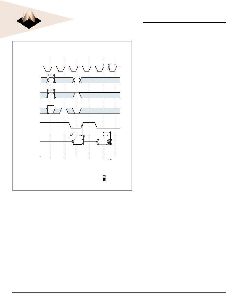
NOTES: WRITE# = L means WE# = L, and BWx# = L
CEx# refers to the combination of CE
1
#, CE
2
, CE
2
#.
Clock
Address
WE
0B
WE
1B
OE
B
#
Data Out
t
CH
t
CL
t
AS
t
AH
A
1
A
2
t
WS
t
WH
t
CSS
t
CSH
t
OE
t
HZOE
t
LZOE
t
CD
t
OH
Q2-1
Q1-1
Don't Care
Undefined
CEx
#
FIG. 3
TIMING WAVEFORM OF READ CYCLE

WED2ZL64512S
October 2001
Rev. 0
6
White Electronic Designs Corporation ∑ (602) 437-1520 ∑ www.wedc.com
White Electronic Designs
White Electronic Designs Corp. reserves the right to change products or specifications without notice.
FIG. 4
TIMING WAVEFORM OF WRITE CYCLE
NOTES: WRITE# = L means WE# = L, and BWx# = L
CEx# refers to the combination of CE
1
#
, CE
2
and CE
2
#
.
Clock
Address
WE
0B
#
WE
1B
Data In
t
CH
t
CL
A
2
D2-1
D1-1
OE
B
#
Data Out
Don't Care
Undefined
A
1
t
HZOE
Q0-3
CEx#
Q0-4

WED2ZL64512S
October 2001
Rev. 0
7
White Electronic Designs Corporation ∑ (602) 437-1520 ∑ www.wedc.com
White Electronic Designs
White Electronic Designs Corp. reserves the right to change products or specifications without notice.
FIG. 5
TIMING WAVEFORM OF SINGLE READ/WRITE
NOTES: WRITE# = L means WE# = L, and BWx# = L
CEx# refers to the combination of CE
1
#, CE
2
and CE
2
#.
Clock
Address
WE
0B
WE
1B
OE
B
#
Data In
t
CH
t
CL
t
DS
t
DH
Data Out
A
2
A
4
A
5
D2
t
OE
t
LZOE
Q1
Don't Care
Undefined
A
1
A
3
A
7
A
6
Q3
Q4
Q7
Q6
D5
A
9
A
8
CEx#

WED2ZL64512S
October 2001
Rev. 0
8
White Electronic Designs Corporation ∑ (602) 437-1520 ∑ www.wedc.com
White Electronic Designs
White Electronic Designs Corp. reserves the right to change products or specifications without notice.
NOTES: WRITE# = L means WE# = L, and BWx# = L
CEx# refers to the combination of CE
1
#, CE
2
and CE
2
#.
Clock
Address
WE
0B
WE
1B
OE
B
#
Data In
t
CH
t
CL
Data Out
A
1
A
2
A
3
A
4
A
5
Don't Care
Undefined
t
CYC
D5
Q4
Q1
Q2
t
OE
t
LZOE
D3
t
CD
t
LZC
t
HZC
t
DH
t
DS
CEx#
FIG. 7
TIMING WAVEFORM OF CE# OPERATION

WED2ZL64512S
October 2001
Rev. 0
9
White Electronic Designs Corporation ∑ (602) 437-1520 ∑ www.wedc.com
White Electronic Designs
White Electronic Designs Corp. reserves the right to change products or specifications without notice.
PACKAGE DIMENSION: 119 BUMP PBGA
ALL LINEAR DIMENSIONS ARE IN MILLIMETERS AND PARENTHETICALLY IN INCHES
1.90 (0.075)
MAX
0.711 (0.028)
MAX
1.27 (0.050)
TYP
1.27 (0.050) TYP
A
B
C
D
E
F
G
H
J
K
L
M
N
P
R
T
U
17.00 (0.669) TYP
A
1
CORNER
20.32 (0.800)
TYP
23.00 (0.905)
TYP
7.62 (0.300)
TYP
ORDERING INFORMATION
Part Number
Configuration
t
CD
(ns)
Clock
(MHz)
WED2ZL64512S35BC
512K x 64
3.5
166
WED2ZL64512S38BC
512K x 64
3.8
150
WED2ZL64512S42BC
512K x 64
4.2
133
WED2ZL64512S50BC
512K x 64
5.0
100
NOTE: Ball attach pad for above BGA package is 620 microns in diameter. Pad is solder mask defined.
COMMERCIAL TEMP RANGE (0∞C TA 70∞C)