1
White Electronic Designs Corporation ∑ (602) 437-1520 ∑ www.wedc.com
White Electronic Designs
WED3C7410E16M-XBX
May 2006
Rev. 9
FEATURES
Footprint compatible with WED3C7558M-XBX and
WED3C750A8M-200BX
Implementation
of
Altivec
TM technology instruction
set
Optional, high-bandwidth MPX bus interface
RISC Microprocessor Multichip Package
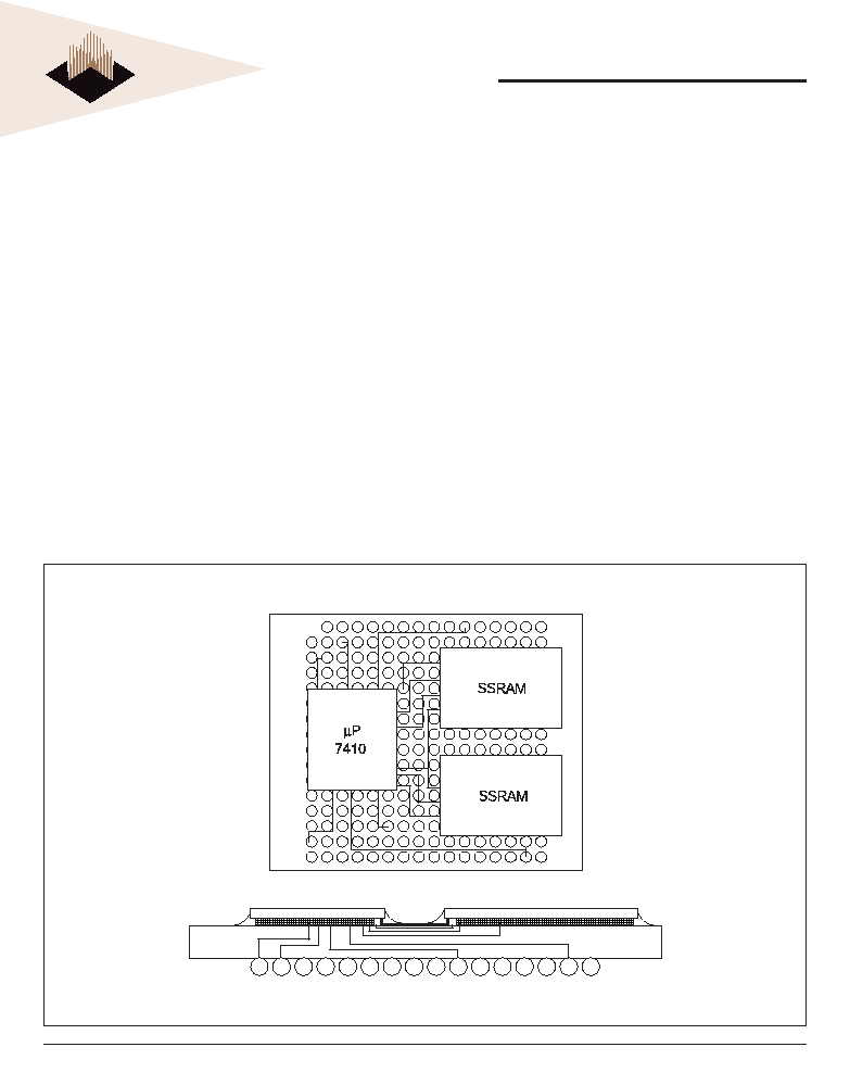
OVERVIEW
The WEDC 7410E/SSRAM multichip package is targeted
for high performance, space sensitive, low power systems
and supports the following power management features:
doze, nap, sleep and dynamic power management.
The WED3C7410E16M-XBX multichip package consists
of:
7410E
AltiVec
TM RISC processor
Dedicated 2MB SSRAM L2 cache, confi gured as
256Kx72
21mmx25mm, 255 Ceramic Ball Grid Array (CBGA)
Maximum Core frequency = 400, 450MHz
Maximum L2 Cache frequency = 200MHz
Maximum 60x Bus frequency = 133MHz**
The WED3C7410E16M-XBX is offered in Commercial
(0∞C to +70∞C), industrial (-40∞C to +85∞C) and military
(-55∞C to +125∞C) temperature ranges and is well suited
for embedded applications such as missiles, aerospace,
fl ight computers, fi re control systems and rugged critical
systems.
* This product is subject to change without notice.
** At a maximum 60x bus frequency of 133MHz, the maximum
confi gurable core frequency is 400MHz.
FIGURE 1 ≠ MULTI-CHIP PACKAGE DIAGRAM
AltiVec
TM is a trademark of Motorola Inc.
2
White Electronic Designs Corporation ∑ (602) 437-1520 ∑ www.wedc.com
White Electronic Designs
WED3C7410E16M-XBX
May 2006
Rev. 9
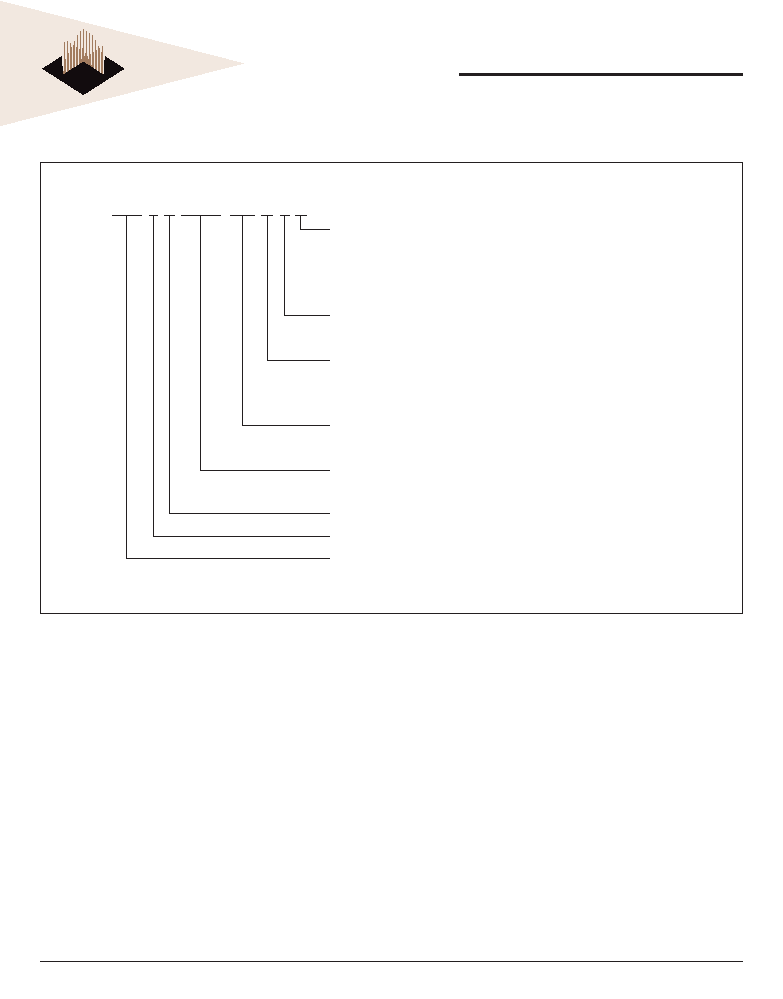
Reservation
Station
Reservation
Station
Fetcher
Dispatch Unit
Reservation
Station
V
e
ctor
Permute
Unit
VSCR
V
e
ctor ALU
VSIU
VCIU
VFPU
Reservation
Station
VR File
6 Rename
Buf
fers
Reservation
Station
Interger
Unit 1
. .
+ x
Interger
Unit 2
. .
GPR File
6 Rename
Buf
fers
. .
FPR File
6 Rename
Buf
fers
. .
System
Register
Unit
V
e
ctor
To
u
c
h
Queue
Reservation
Station
Floating-Point
Unit
Reservation
Station (2 Entry)
Load/Store Unit
(EA
Calculation)
Finished
Stores
Complete
Stores
L1
Operations
Load Fold
Queue
+
+
. .
+ x
FPSCR
Additional Features
T
i
me Base
Counter/Decrementer
Clock Muliplier
JT
AG/COP
Interface
Thermal/Power Management
Performance Monitor
Instruction Queue
(6 W
ord)
Completion Queue
(8 Entry)
Completion Unit
Branch Processing Unit
BTIC
(64 Entry)
BHT
(512 Entry)
LR
CTR
Instruction MMU
SRs
(Shadow)
128-Entry
DTLB
IBA
T
Array
Data MMU
SRs
(Original)
128-Entry
DTLB
DBA
T
Array
Ta
g
s
32-Kbyte
I Cache
Ta
g
s
32-Kbyte
I Cache
Ability to complete up
to two instructions per clock
L2 Data
T
ransaction
Queue
L2 Controller
L2 T
ags
L2CR
L2PMCR
L2 Miss
L2 Castout
Data
T
ransaction
Queue
Bus Interface Unit
Data Reload
Buf
fer
Instruction
Reload Buf
fer
Instruction
Reload T
able
Data Reload
Ta
b
l
e
Memory Subsystem
SSRAM
S
SRAM
19-Bit L2 Address Bus
64- 32-Bit L2 Data Bus
64-Bit Data Bus
32-Bit Address Bus
32-Bit
32-Bit
32-Bit
64-Bit
64-Bit
128-Bit
128-Bit
EA
PA
128-Bit
(4 Instructions)
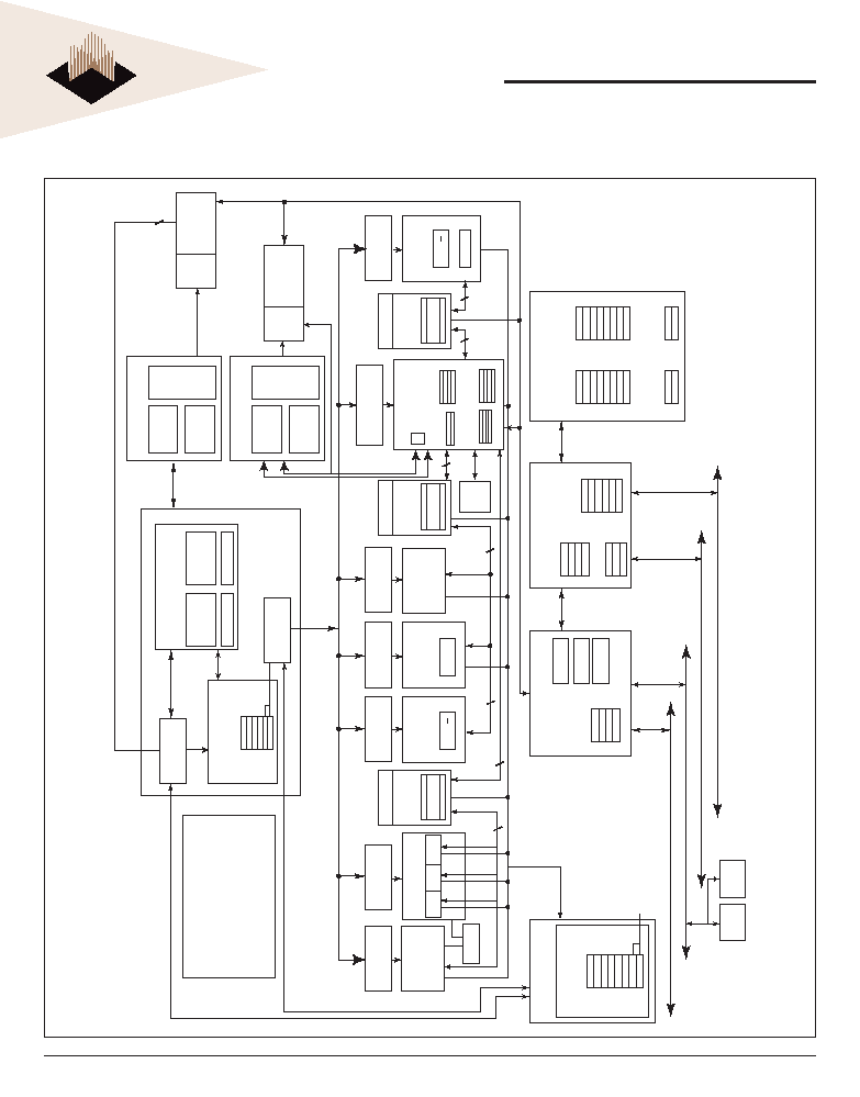
FIGURE 2 ≠ BLOCK DIAGRAM
3
White Electronic Designs Corporation ∑ (602) 437-1520 ∑ www.wedc.com
White Electronic Designs
WED3C7410E16M-XBX
May 2006
Rev. 9
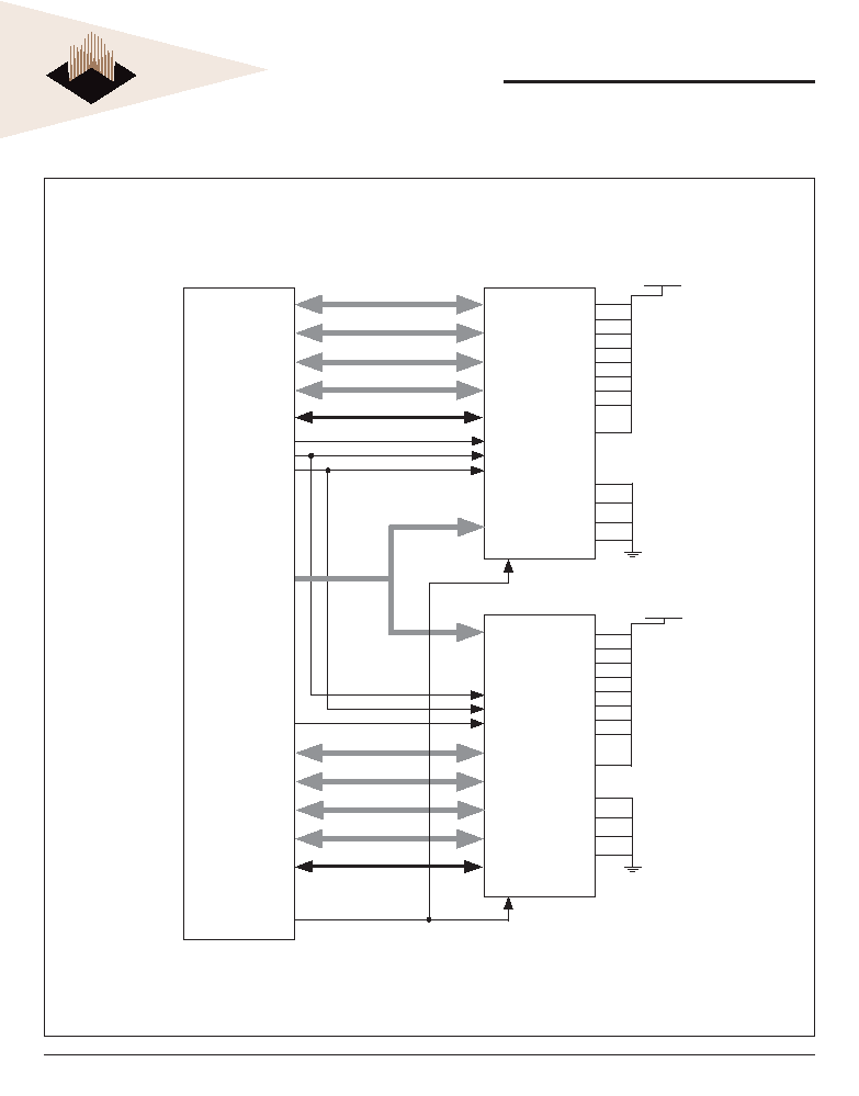
FIGURE 3 ≠ BLOCK DIAGRAM, L2 INTERCONNECT
L2pin_DATA
L2pin_DATA
L2pin_DATA
L2pin_DATA
L2 CLK_OUT A
L2WE#
L2CE#
A
0-17
L2CLK_OUT B
L2pin_DATA
L2pin_DATA
L2pin_DATA
L2pin_DATA
L2ZZ
µP
7410E
DQa
DQb
DQc
DQd
K
SGW#
SE1#
SA
0-17
SA
0-17
SGW#
SE1#
K
DQa
DQb
DQc
DQd
SSRAM 1
SSRAM 2
FT#
SBd#
SBc#
SBb#
SBa#
SW#
ADSP#
ADV#
SE2
ADSC#
SE3#
LBO#
G#
FT#
SBd#
SBc#
SBb#
SBa#
SW#
ADSP#
ADV#
SE2
ADSC#
SE3#
LBO#
G#
L2Vdd
L2Vdd
L2DP0-3
DP0-3
L2DP4-7
DP0-3
ZZ
ZZ
U2
U1
4
White Electronic Designs Corporation ∑ (602) 437-1520 ∑ www.wedc.com
White Electronic Designs
WED3C7410E16M-XBX
May 2006
Rev. 9
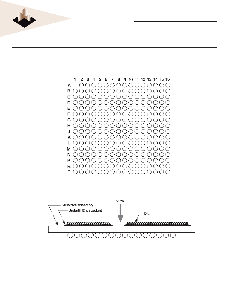
FIGURE 5 ≠ PIN ASSIGNMENTS
Ball assignments of the 255 CBGA package as viewed from the top surface.
Side profi le of the CBGA package to indicate the direction of the top surface view.
5
White Electronic Designs Corporation ∑ (602) 437-1520 ∑ www.wedc.com
White Electronic Designs
WED3C7410E16M-XBX
May 2006
Rev. 9
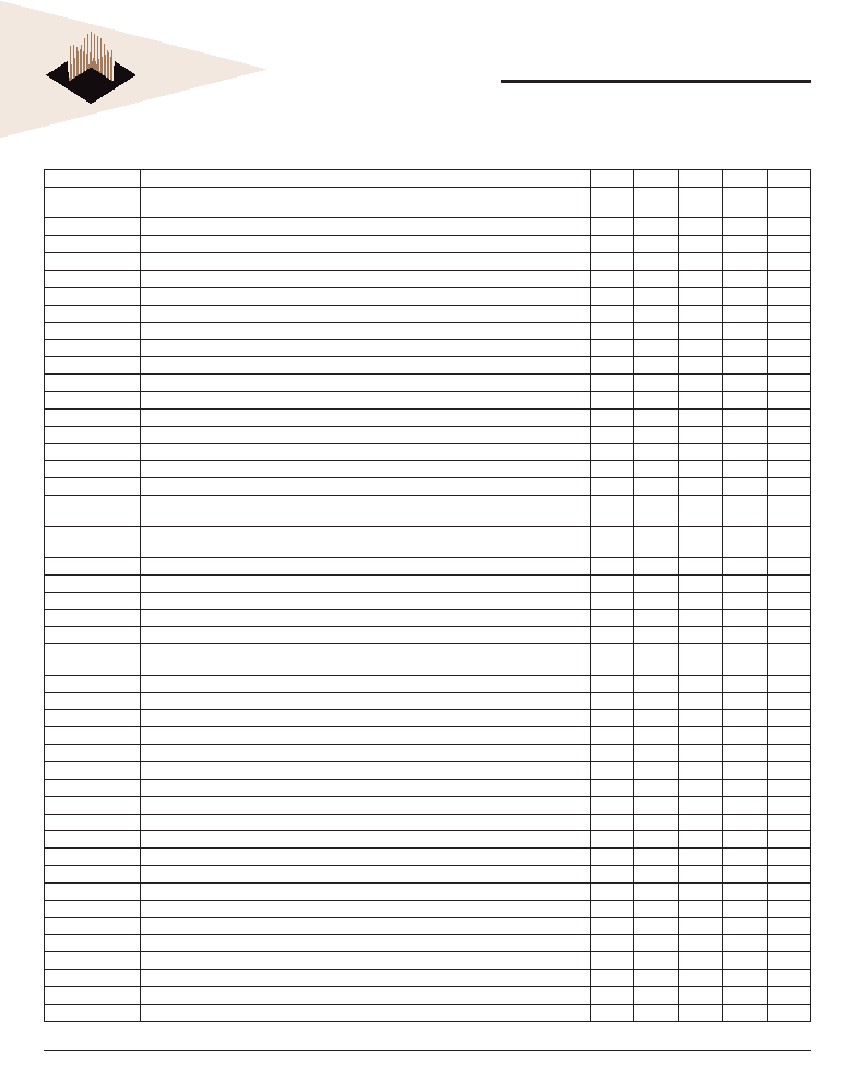
PACKAGE PINOUT LISTING
Signal Name
Pin Number
Active
I/O
1.8V (7) 2.5V (7)
3.3V (7)
A[0-31]
C16, E4, D13, F2, D14, G1, D15, E2, D16, D4, E13, G2, E15, H1, E16, H2, F13, J1, F14, J2, F15, H3,
F16, F4, G13, K1, G15, K2, H16, M1, J15, P1
High
I/O
AACK#
L2
Low Input
ABB#/AMONO# (8)
K4
Low
Output
AP[0-3]
C1, B4, B3, B2
High I/O
ARTRY# J4
Low I/O
AVCC A10
-- Input
1.8V 1.8V 1.8V
BG# L1
Low Input
BR# B6
Low Output
BVSEL (4, 6)
B1
High Input GND
HRESET# OVCC
CHK# (5, 6, 13)
C6
Low Input
CI# E1
Low I/O
CKSTP_IN# D8
Low Input
CKSTP_OUT# A6
Low Ouput
CLK_OUT
D7
High
Output
DBB#/DMONO (8)
J14
Low Output
DBG# N1
Low Input
DBWO#/DTI[0] G4
Low Input
DH[0-31]
P14, T16, R15, T15, R13, R12, P11, N11, R11, T12, T11, R10, P9, N9, T10, R9, T9, P8, N8, R8, T8, N7,
R7, T7, P6, N6, R6, T6, R5, N5, T5, T4
High I/O
DL[0-31]
K13, K15, K16, L16, L15, L13, L14, M16, M15, M13, N16, N15, N13, N14, P16, P15, R16, R14, T14,
N10, P13, N12, T13, P3, N3, N4, R3, T1, T2, P4, T3, R4
High I/O
DP[0-7]
M2, L3, N2, L4, R1, P2, M4, R2
High
I/O
DRDY# (5, 9, 12)
D5
Low Output
DTI 1-2 (9, 11)
G16, H15
High Input
EMODE# (10, 11)
C4
Low Input
GBL# F1
Low I/O
GND
C5, C12, E3, E6, E8, E9, E11, E14, F3, F5, F7, F10, F12, G6, G8, G9, G11, H5, H7, H10, H12, J5, J7,
J10, J12, K6, K8, K9, K11, L5, L7, L10, L12, M3, M6, M8, M9, M11, M14, P5, P12
-- --
GND
GND
GND
HIT# (5) (12)
A3
Low Output
HRESET# A7
Low Input
INT# B15
Low Input
L1_TSTCLK (1)
D11
High Input
L2_TSTCLK (1)
D12
High Input
L2AVCC L11
-- Input 1.8V 1.8V
1.8V
L2VCC (5) (7)
A2, B8, C3, D6, J16
-- Input 3.3V 3.3V
3.3V
L2OVCC
E10, E12, M12, G12, G14, K12, K14
--
Input
2.5V
N/A
L2VSEL (3, 6)
B5
High Input *--
HRESET#
N/A
LSSD_MODE# (1)
B10
Low Input
3.3V
MCP# C13
Low Input
NC (No-connect)
B7, C8
--
--
OVCC (2)
C7, E5, G3, G5, K3, K5, P7, P10, E7, M5, M7, M10
--
Input
1.8V
2.5V
3.3V
PLL_CFG[0-3]
A8, B9, A9, D9
High Input
QACK# D3
Low Input
QREQ# J3
Low Output
RSRV# D1
Low Output
SHD0-1# (5) (14)
A4, A5
Low I/O
SMI# A16
Low Input
SRESET# B14
Low Input

6
White Electronic Designs Corporation ∑ (602) 437-1520 ∑ www.wedc.com
White Electronic Designs
WED3C7410E16M-XBX
May 2006
Rev. 9
Signal Name
Pin Number
Active
I/O
1.8V (7) 2.5V (7) 3.3V (7)
SYSCLK C9
-- Input
TA# H14
Low Input
TBEN C2
High Input
TBST# A14
Low Output
TCK C11
High Input
TDI (6)
A11
High Input
TDO A12
High Output
TEA# H13
Low
Input
TMS (6)
B11
High Input
TRST# (6)
C10
Low Input
TS# J13
Low I/O
TSIZ[0-2]
A13, D10, B12
High Output
TT[0-4]
B13, A15, B16, C14, C15
High
I/O
V
CC
(2)
F6, F8, F9, F11, G7, G10, H4, H6, H8, H9, H11, J6, J8, J9, J11, K7, K10, L6, L8, L9
--
Input
1.8V
1.8V
1.8V
WT# D2
Low I/O
PACKAGE PINOUT LISTING (continued)
NOTES:
1.
These are test signals for factory use only and must be pulled up to OV
CC
for
normal machine operation.
2. OV
CC
inputs supply power to the I/O drivers and V
CC
inputs supply power to the
processor core.
3.
To allow future L2 cache I/O interface voltage changes.
4.
To allow processor bus I/O voltage changes, provide the option to connect BVSEL
to HRESET# (Selects 2.5V Interface) or to GND (Selects 1.8V Interface) or to
OV
CC
(Selects 3.3V Interface).
5.
Uses one of 9 existing no-connects in WEDC's WED3C755A8M-XBX.
6.
Internal pull up on die.
7. OV
CC
supplies power to the processor bus, JTAG, and all control signals except
the L2 cache controls (L2CE, L2WE, and L2ZZ); L2OV
CC
supplies power to the L2
cache I/O interface (L2ADDR (0-18], L2DATA (0-63), L2DP{0-7] and L2SYNC-
OUT) and the L2 control signals; L2AV
CC
supplies power to the SSRAM core
memory; and V
CC
supplies power to the processor core and the PLL and DLL (after
fi ltering to become AV
CC
and L2AV
CC
respectively). These columns serve as a
reference for the nominal voltage supported on a given signal as selected by the
BVSEL pin confi guration and the voltage supplied. For actual recommended value
of Vin or supply voltages see Recommended Operating Conditions.
8.
Output only for 7410, was I/O for 750/755.
9.
Enhanced mode only.
10. Deasserted (pulled high) at HRESET# for 60x bus mode.
11. Reuses 750/755 DRTRY#, DBIS#, and TLBISYNC pins (DTI1, DTI2, and EMODE#
respectively).
12. Unused output in 60x bus mode.
13. Connect to HRESET# to trigger post power-on-reset (por) internal memory test.
14. Ignored in 60x bus mode.

7
White Electronic Designs Corporation ∑ (602) 437-1520 ∑ www.wedc.com
White Electronic Designs
WED3C7410E16M-XBX
May 2006
Rev. 9
ABSOLUTE MAXIMUM RATINGS
Characteristic
Symbol
Value
Unit
Notes
Core supply voltage
V
CC
-0.3 to 2.1
V
(4)
PLL supply voltage
AV
CC
-0.3 to 2.1
V
(4)
L2 DLL supply voltage
L2AV
CC
-0.3 to 2.1
V
(4)
60x bus supply voltage
OV
CC
-0.3 to 3.465
V
(3)
L2 bus supply voltage
L2OV
CC
-0.3 to 2.6
V
(3)
L2 supply voltage
L2V
CC
-0.3 to 4.6
V
(5)
Input supply
Processor Bus
V
IN
-0.3 to 0V
CC
+0.2
V
(2)
L2 bus
V
IN
-0.3 to L20V
CC
+0.2
V
(2)
JTAG Signals
V
IN
-0.3 to OV
CC
+0.2
V
(2)
Storage temperature range
T
STG
-55 to 150
∞C
NOTES:
1. Functional and tested operating conditions are given in Operating Conditions table. Absolute maximum ratings are stress ratings only, and functional operation at the maximums is
not guaranteed. Stresses beyond those listed may affect device reliability or cause permanent damage to the device.
2. Caution:
Vin must not exceed OV
CC
by more than 0.2V at any time including during power-on reset.
3. Caution:
OV
CC
/L2OV
CC
must not exceed V
CC
/AV
CC
/L2AV
CC
by more than 2.0 V at any time including during power-on reset.
4. Caution:
V
CC
/AV
CC
/L2AV
CC
must not exceed L2OV
CC
/OV
CC
by more than 0.4 V at any time including during power-on reset.
5. L2OV
CC
should never exceed L2V
CC
RECOMMENDED OPERATING CONDITIONS
CHARACTERISTIC SYMBOL
RECOMMENDED
VALUE
UNIT
Core supply voltage
V
CC
1.8v
±
100mV
V
PLL supply voltage
AV
CC
1.8v
±
100mV
V
L2 DLL supply voltage
L2AV
CC
1.8v
±
100mV
V
Memory core supply voltage
L2V
CC
3.3v
±
165mV
V
Processor bus supply voltage
BVSEL = 0
OV
CC
1.8±
100mV
V
BVSEL = HRESET#
OV
CC
2.5v
±
100mV
V
BVSEL = HRESET or BVSEL = 1
OV
CC
3.3v ± 165 mV
V
L2 bus supply voltage
L2VSEL = HRESET# or 1
L20V
CC
2.5v ± 100 mV
V
Input Voltage
Processor bus and JTAG Signals
Vin
GND to OV
CC
V
NOTE: These are the recommended and tested operating conditions. Proper device operation outside of these conditions is not guaranteed

8
White Electronic Designs Corporation ∑ (602) 437-1520 ∑ www.wedc.com
White Electronic Designs
WED3C7410E16M-XBX
May 2006
Rev. 9
L2 CACHE CONTROL REGISTER (L2CR)
The L2 cache control register, shown in Figure 5, is a supervisor-level, implementation-specifi c SPR used to confi gure
and operate the L2 cache. It is cleared by hard reset or power-on reset.
BGA THERMAL RESISTANCE
Description
Symbol
PPC
SSRAM Units
Notes
Junction to Ambient (No Airfl ow)
Theta JA
14.0
10.3
C/W
1
Junction to Ball
Theta JB
8.9
5.2
C/W
1
Junction to Case (Top)
Theta JC
0.1
0.1
C/W
1
NOTE 1: Refer to PBGA Thermal Resistance Correlation at www.whiteedc.com in the application notes section for modeling conditions
POWER CONSUMPTION
V
CC
= AV
CC
= 1.8 ±0.1V V
DC
, L2V
CC
= 3.3V ±5% V
DC
, GND = 0 V
DC
, 0
T
J
< 105∞C
Processor (CPU) Frequency/L2 Frequency
Unit Notes
400MHz/200MHz
450MHz/200MHz
Full-on Mode
Typical
5.7
6.2
W
1, 3
Maximum 13.1 14.3
W
1,
2
Doze Mode
Maximum
5.3
5.8
W
1, 2
Nap Mode
Maximum
2.25
2.4
W
1, 2
Sleep Mode
Maximum
2.20
2.35
W
1, 2
Sleep Mode≠PLL and DLL Disabled
Maximum
2.0
2.0
W
1, 2
NOTES:
1. These values apply for all valid system bus and L2 bus ratios. The values do not include OV
CC
; AV
CC
and L2AV
CC
suppling power. OV
CC
power is system dependent, but is typically
<10% of V
CC
power. Worst case power consumption, for AV
CC
= 15mW and L2AV
CC
= 15mW.
2. Maximum power is measured at V
CC
= 1.9 V while running an entirely cache-resident, contrived sequence of instructions which keep the execution units maximally busy.
3. Typical power is an average value measured at V
CC
= AV
CC
= L2AV
CC
= 1.8V, OV
CC
d = L2OV
CC
= 2.5V in a system, executing typical applications and benchmark sequences.
4.
At a maximum 60x bus frequency of 133MHz, the maximum confi gurtable core frequency is 400MHz.
FIGURE 5 ≠ L2 CACHE CONTROL REGISTER (L2CR)
The L2CR bits are described in Table 1.
L2E
L2SIZ
L2CLK
L2RAM
L21
L2OH 0000000
0
1
2
3
4
6
7
8
9
10 11 12 13 14 15 16 17 18 19 20 21 22 22 24 30 31
L2IP
L2PE
L2DO
L2CTL
L2TS
L2SL
L2BYP
L2HWF
L2IO
L2DRO
L2WT L2DF
L2FA
L2CLKSTP

9
White Electronic Designs Corporation ∑ (602) 437-1520 ∑ www.wedc.com
White Electronic Designs
WED3C7410E16M-XBX
May 2006
Rev. 9
TABLE 1: L2CR BIT SETTINGS
Bit
Name
Function
0
L2E
L2 enable. Enables L2 cache operation (including snooping) starting with the next transaction the L2 cache unit receives.
Before enabling the L2 cache, the L2 clock must be confi gured through L2CR[2CLK], and the L2 DLL must stabilize. All other
L2CR bits must be set appropriately. The L2 cache may need to be invalidated globally.
1
L2PE
L2 data parity checking enable. Enables parity generation and checking for the L2 data RAM interface. When disabled,
generated parity is always zeros. L2 Parity is supported by WEDC's WED3C7410E16M-XBX, but is dependent on application.
2≠3
L2SIZ
L2 size--Should be set according to the size of the private memory setting. Total SRAM space is 2M bytes (256Kx72). See L2
cache/private memory confi gurations table in Motorola User's Manual.
4≠6
L2CLK
L2 clock ratio (core-to-L2 frequency divider). Specifi es the clock divider ratio based from the core clock frequency that the
L2 data RAM interface is to operate at. When these bits are cleared, the L2 clock is stopped and the on-chip DLL for the L2
interface is disabled. For nonzero values, the processor generates the L2 clock and the on-chip DLL is enabled. After the L2
clock ratio is chosen, the DLL must stabilize before the L2 interface can be enabled. The resulting L2 clock frequency cannot be
slower than the clock frequency of the 60x bus interface.
000 L2 clock and DLL disabled
001
˜ 1
010
˜ 1.5
011
˜ 3.5
100
˜ 2
101
˜ 2.5
110
˜ 3
111
˜ 4
7≠8
L2RAM
L2 RAM type--Confi gures the L2 RAM interface for the type of synchronous SRAMs used:
∑ Pipelined (register-register) synchronous burst SRAMs that clock addresses in and clock data out
The 7410 does not burst data into the L2 cache, it generates an address for each access.
10: Pipelined (register-register) synchronous burst SRAM - Setting for WED3C7410E16M-XBX
9
L2DO
L2 data only. Setting this bit enables⁄data-only operation in the L2 cache. When this bit is set, only transactions from the L1
data cache can be cached in the L2 cache. L1 instruction cache operations will be serviced for instruction addresses already
in the L2 cache; however, the L2 cache will not be reloaded for L1 instruction cache misses. Note that setting both L2DO and
L2IO effectively locks the L2 cache.
10
L2I
L2 global invalidate. Setting L2I invalidates the L2 cache globally by clearing the L2 status bits. This bit must not be set while
the L2 cache is enabled. See
Motorola's User manual for L2 Invalidation procedure.
11
L2CTL
L2 RAM control (ZZ enable). Setting L2CTL enables the automatic operation of the L2ZZ (low-power mode) signal for cache
RAMs. Sleep mode is supported by the WED3C7410E16M-XBX. While L2CTL is asserted, L2ZZ asserts automatically when
the device enters nap or sleep mode and negates automatically when the device exits nap or sleep mode. This bit should not
be set when the device is in nap mode and snooping is to be performed through deassertion of QACK.
12
L2WT
L2 write-through. Setting L2WT selects write-through mode (rather than the default write-back mode) so all writes to the L2
cache also write through to the system bus. For these writes, the L2 cache entry is always marked as clean (value unmodifi ed)
rather than dirty (value modifi ed). This bit must never be asserted after the L2 cache has been enabled as previously-modifi ed
lines can get remarked as clean (value unmodifi ed) during normal operation.
13
L2TS
L2 test support. Setting L2TS causes cache block pushes from the L1 data cache that result from dcbf and dcbst
instructions to be written only into the L2 cache and marked valid, rather than being written only to the system bus and marked
invalid in the L2 cache in case of hit. This bit allows a dcbz/dcbf instruction sequence to be used with the L1 cache enabled
to easily initialize the L2 cache with any address and data information. This bit also keeps dcbz instructions from being
broadcast on the system and single-beat cacheable store misses in the L2 from being written to the system bus.
14≠15
L2OH
L2 output hold. These bits confi gure output hold time for address, data, and control signals driven to the L2 data RAMs.
01: 0.8ns Hold Time - Setting for WED3C7410E16M-XBX

10
White Electronic Designs Corporation ∑ (602) 437-1520 ∑ www.wedc.com
White Electronic Designs
WED3C7410E16M-XBX
May 2006
Rev. 9
Bit
Name
Function
16
L2SL
L2 DLL slow. Setting L2SL increases the delay of each tap of the DLL delay line. It is intended to increase the delay through the
DLL to accommodate slower L2 RAM bus frequencies.
0: Setting for WED3C7410E16M-XBX because L2 RAM interface is operated above 100 MHz.
17
L2DF
L2 differential clock. This mode supports the differential clock requirements of late-write SRAMs.
0: Setting for WED3C7410E16M-XBX because late-write SRAMs are not used.
18
L2BYP
L2 DLL bypass is reserved.
0: Setting for WED3C7410E16M-XBX
19
L2FA
L2 fl ush assist (for software fl ush). When this bit is negated, all lines castout from the dL1 which have a state of
CDMRSV=01xxx1 (i.e. C-bit negated), will not allocate in the L2 if they miss. Asserting this bit forces every castout from the dL1
to allocate an entry in the L2 if that castout misses in the L2 regardless of the state of the C-bit. The L2FA bit must be set and
the L2IO bit must be cleared in order to use the software fl ush algorithm.
20
L2HWF
L2 hardware fl ush. When the processor detects the value of L2HWF set to 1, the L2 will begin a hardware fl ush. The fl ush will
be done by starting with low cache indices and increment these indices for way 0 of the cache, one index at a time until the
maximum index value is obtained. Then, the index will be cleared to zero and the same process is repeated for way 1 of the
cache. For each index and way of the cache, the processor will generate a castout operation to the system bus for all modifi ed
32-byte sectors. At the end of the hardware fl ush, all lines in the L2 tag will be invalidated. During the fl ush, all memory activity
from the icache and dcache are blocked from accessing the L2 until the fl ush is complete. Snoops, however, are fully serviced
by the L2 during the fl ush. When the L2 tags have been fully fl ushed of all valid entries, this bit will be reset to b'0" by hardware.
When this bit is cleared, it does not necessarily guarantee that all lines form the L2 have been written completely to the system
interface. L2 copybacks can stll be queued in the bus interface unit. Below is the code which must be run to use L2 Hardware
Flush. When the fi nal sync completes, all modifi ed lines in the L2 will have been written to the system
address bus.
Disable interrupts
dssall
sync
set L2HWF
sync
21
L2IO
L2 Instruction-Only. Setting this bit enales instruction-only operation in the L2 cache. For this operation, only transactions from
the L1 instruction cache are allowed to be reloaded in the L2 cache. Data addresses already in the cache will still hit for the L1
data cache. When both L2DO and L2IO are asserted, the L2 cache is effectively locked.
22
L2CLKSTP
L2 Clock Stop. Setting this bit enables the automatic stopping of the L2CLK_OUT signals for cache rams that support this
function. While L2CLKSTP is set, the L2CLK_OUT signals will automatically be stopped when WED3C7410E16M-XBX enters
nap or sleep mode, and automatically restarted when WED3C7410E16M-XBX exits nap or sleep.
23
L2DRO
L2 DLL rollover. Setting this bit enables a potential rollover (or actual rollover) condition of the DLL to cause a checkstop for the
processor. A potential rollover condition occurs when the DLL is selecting the last tap of the delay line, and thus may risk rolling
over to the fi rst tap with one adjustment while in the process of keeping synchronized. Such a condition is improper operation
for the DLL, and, while this condition is not expected, it allows detection for added security. This bit can be set when the DLL is
fi rst enabled (set with the L2CLK bits) to detect rollover during initial synchronization. It could also be set when the L2 cache is
enabled (with L2E bit) after the DLL has achieved its initial lock.
24≠30 -
Reserved
31
L2IP
L2 global invalidate in progress (read only)--See the Motorola user's manual for L2 Invalidation procedure.
TABLE 1: L2CR BIT SETTINGS
11
White Electronic Designs Corporation ∑ (602) 437-1520 ∑ www.wedc.com
White Electronic Designs
WED3C7410E16M-XBX
May 2006
Rev. 9
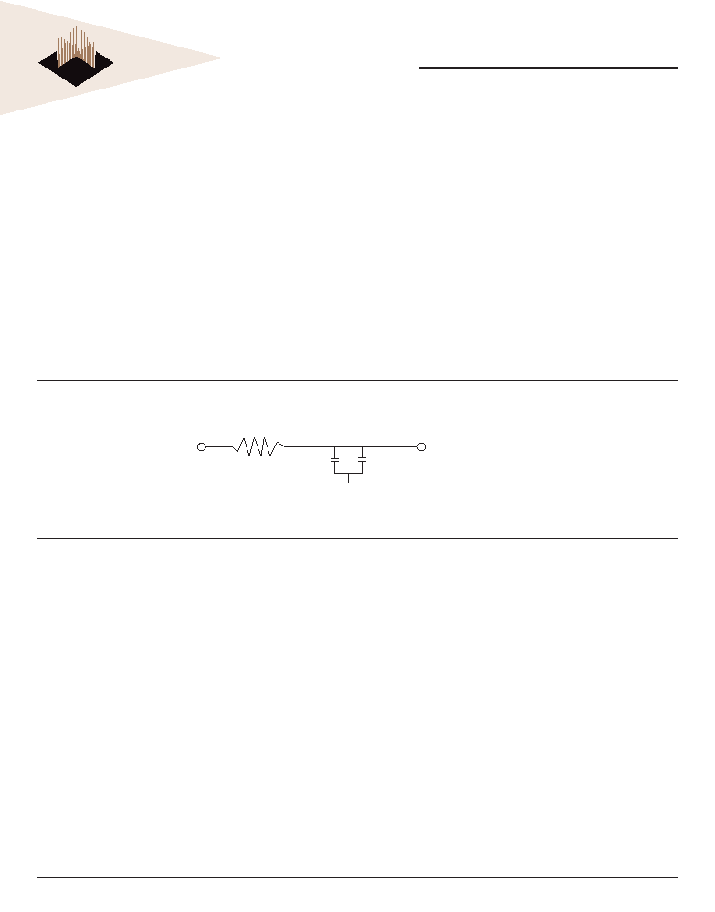
The AVCC and L2AVCC power signals are provided on
the WED3C7410E16M-XBX to provide power to the clock
generation phase-locked loop and L2 cache delay-locked
loop respectively. To ensure stability of the internal clock,
the power supplied to the AVCC input signal should be
fi ltered of any noise in the 500kHz to 10 MHz resonant
frequency range of the PLL. A circuit similar to the
one shown in Figure 6 using surface mount capacitors
with minimum Effective Series Inductance (ESL) is
recommended. Multiple small capacitors of equal value are
recommended over a single large value capacitor.
PLL POWER SUPPLY FILTERING
The circuit should be placed as close as possible to the
AVCC pin to minimize noise coupled from nearby circuits.
An identical but separate circuit should be placed as close
as possible to the L2AVCC pin. It is often possible to route
directly from the capacitors to the AVCC pin, which is on the
periphery of the 255 BGA footprint, without the inductance
of vias. The L2AVCC pin may be more diffi cult to route but
is proportionately less critical.
FIGURE 6 ≠ POWER SUPPLY FILTER CIRCUIT
AV
CC
(or L2AV
CC
)
2.2
µF
2.2
µF
GND
Low ESL surface mount capacitors
V
CC
10
12
White Electronic Designs Corporation ∑ (602) 437-1520 ∑ www.wedc.com
White Electronic Designs
WED3C7410E16M-XBX
May 2006
Rev. 9
Package Outline
21x25mm
Interconnects
255 (16x16 ball array less one)
Pitch 1.27mm
Maximum module height
3.90mm
Ball diameter
0.8mm
PACKAGE DIMENSIONS 255 BALL GRID ARRAY
PACKAGE DESCRIPTION
NOTES:
1.
Dimensions in millimeters and paranthetically in inches.
2.
A1 corner is designated with a ball missing the array.
2.20 (0.087)
MAX
T
R
P
N
M
L
K
J
H
G
F
E
D
C
B
A
1 2 3 4 5 6 7 8 9 10 11
12 13 14 15
16
BOTTOM VIEW
TOP VIEW
13
White Electronic Designs Corporation ∑ (602) 437-1520 ∑ www.wedc.com
White Electronic Designs
WED3C7410E16M-XBX
May 2006
Rev. 9
WED 3 C 7410E 16M X B X
DEVICE GRADE:
M = Military Screened
-55∞C to +125∞C
I = Industrial
-40∞C to +85∞C
C = Commercial
0∞C to +70∞C
PACKAGE TYPE:
B = 255 Ceramic Ball Grid Array
CORE FREQUENCY (MHz)
400
=
400MHz
450
=
450MHz
L2 CACHE DENSITY:
16Mbits = 256K x 72 SSRAM
PowerPC
TM:
Type
7410E
C = MULTICHIP PACKAGE
3 = PowerPC
TM
WHITE ELECTRONIC DESIGNS CORP.
ORDERING INFORMATION
PowerPC
TM is a trademark of International Business Machine Corp.