1
White Electronic Designs Corporation (602) 437-1520 www.whiteedc.com
WED3C750A8M-200BX
White Electronic Designs
NOT
RECOMMENDED
FOR
NEW
DESIGNS*
RISC Microprocessor Module
October 2002 Rev. 9
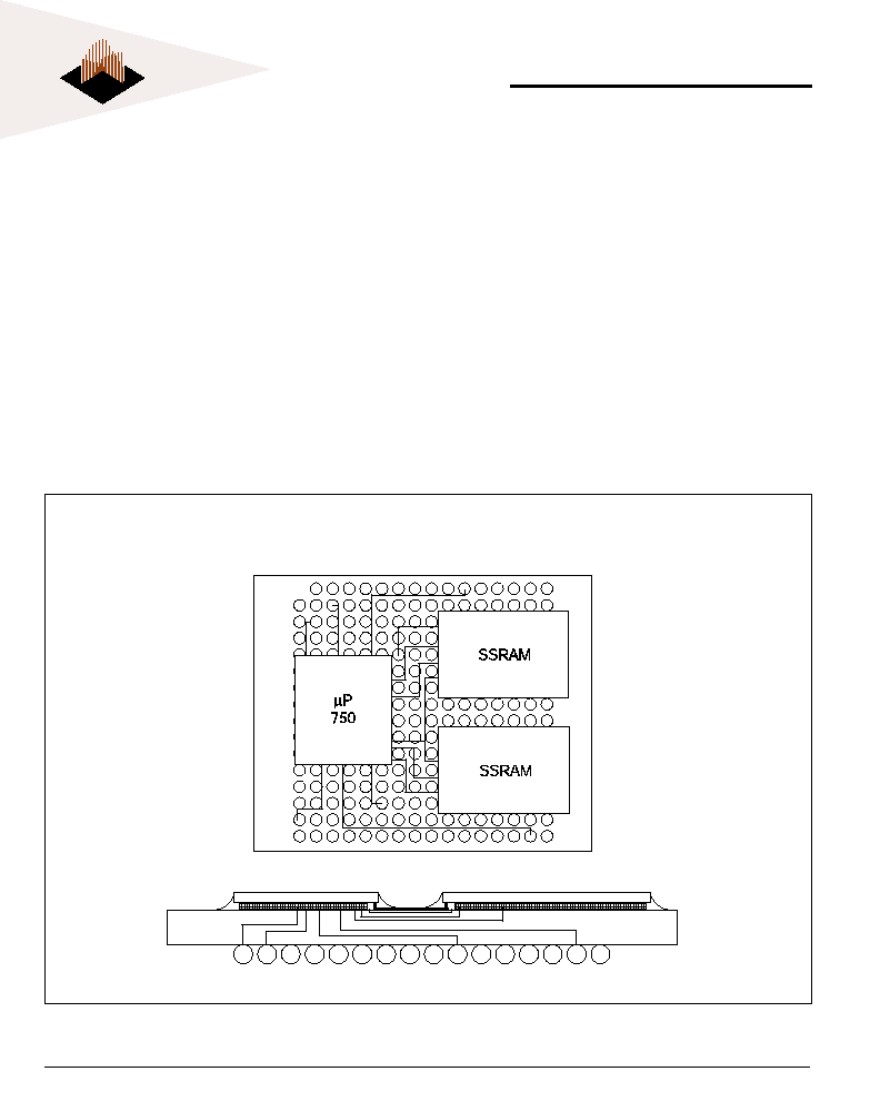
FIG. 1 MULTI-CHIP PACKAGE DIAGRAM
OVERVIEW
The WEDC 750/SSRAM module is targeted for high
performance, space sensitive, low power systems and
supports the following power management features:
doze, nap, sleep and dynamic power management.
The WED3C750A8M-200BX multi-chip package con-
sists of:
750 RISC processor
Dedicated 1MB SSRAM L2 cache, configured as
128Kx72
21mmx25mm, 255 Ceramic Ball Grid Array (CBGA)
Maximum Core frequency = 200MHz
Maximum L2 Cache frequency = 100MHz
Maximum 60x Bus frequency = 66MHz
The WED3C750A8M-200BX is offered in industrial (-
40∞C to +85∞C) and military (-55∞C to +125∞C) tem-
perature ranges and is well suited for embedded ap-
plications such as missiles, aerospace, flight comput-
ers, fire control systems and rugged critical systems.
* This data sheet describes a product that is not recommended for
new designs.
2
White Electronic Designs Corporation Phoenix AZ (602) 437-1520
WED3C750A8M-200BX
White Electronic Designs
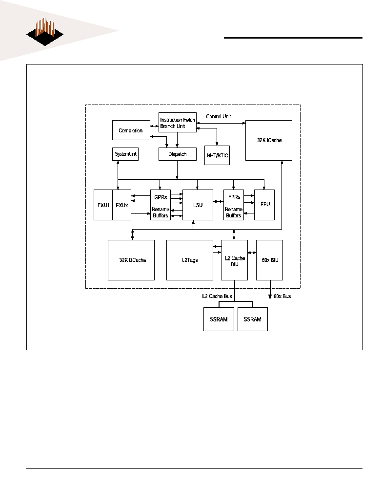
FIG. 2 BLOCK DIAGRAM
3
White Electronic Designs Corporation (602) 437-1520 www.whiteedc.com
WED3C750A8M-200BX
White Electronic Designs
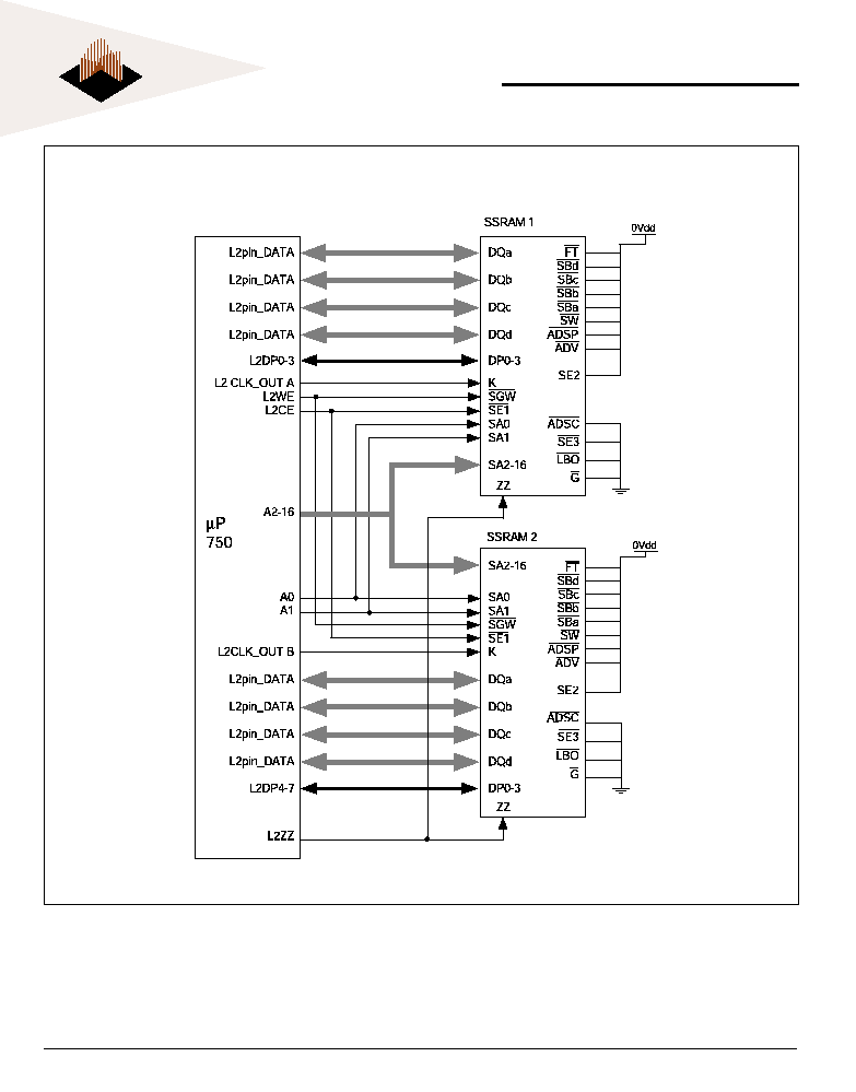
FIG. 3 BLOCK DIAGRAM, L2 INTERCONNECT
4
White Electronic Designs Corporation Phoenix AZ (602) 437-1520
WED3C750A8M-200BX
White Electronic Designs
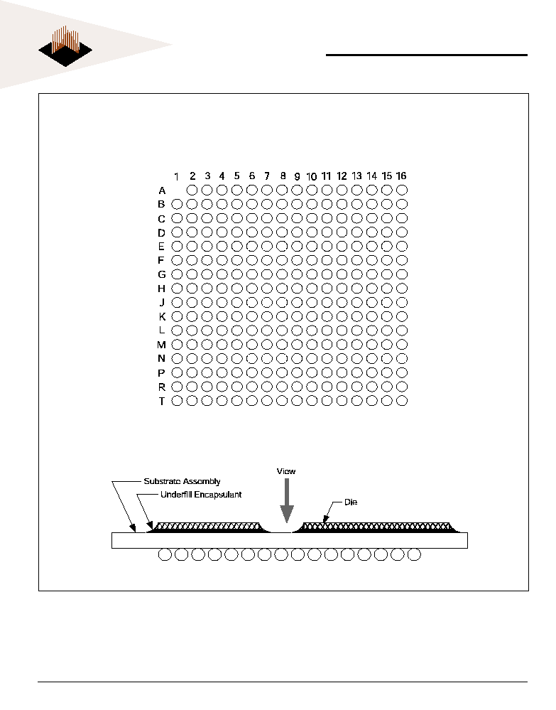
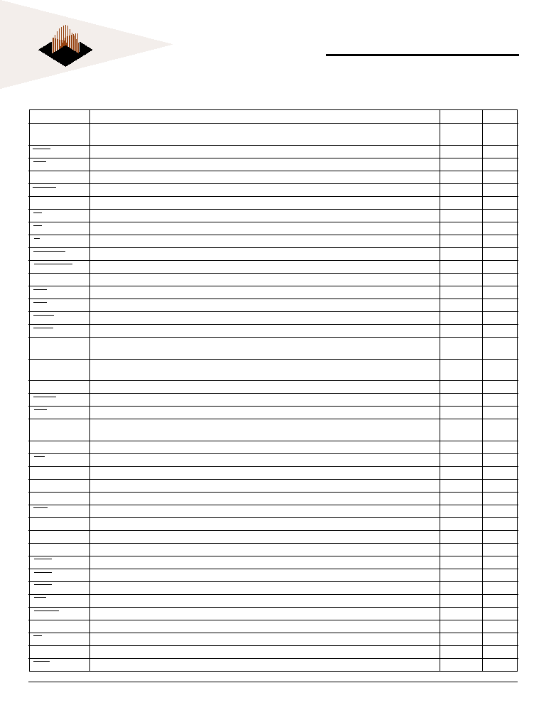
FIG. 4 PIN ASSIGNMENTS
Ball assignments of the 255 CBGA package as viewed from the top surface.
Side profile of the CBGA package to indicate the direction of the top surface view.
5
White Electronic Designs Corporation (602) 437-1520 www.whiteedc.com
WED3C750A8M-200BX
White Electronic Designs
Signal Name
Pin Number
Active
I/O
A[0-31]
C16, E4, D13, F2, D14, G1, D15, E2, D16, D4, E13, G2, E15, H1, E16, H2, F13, J1, F14, J2, F15, H3,
High
I/O
F16, F4, G13, K1, G15, K2, H16, M1, J15, P1
AACK
L2
LowInput
ABB
K4
LowI/O
AP[0-3]
C1, B4, B3, B2
High
I/O
ARTRY
J4
LowI/O
AVDD
A10
BG
L1
LowInput
BR
B6
LowOutput
CI
E1
LowOutput
CKSTP_IN
D8
LowInput
CKSTP_OUT
A6
LowOuput
CLK_OUT
D7
Output
DBB
J14
LowI/O
DBG
N1
LowInput
DBDIS
H15
LowInput
DBWO
G4
LowInput
DH[0-31]
P14, T16, R15, T15, R13, R12, P11, N11, R11, T12, T11, R10, P9, N9, T10, R9, T9, P8, N8, R8, T8, N7,
High
I/O
R7, T7, P6, N6, R6, T6, R5, N5, T5, T4
DL[0-31]
K13, K15, K16, L16, L15, L13, L14, M16, M15, M13, N16, N15, N13, N14, P16, P15, R16, R14, T14,
High
I/O
N10, P13, N12, T13, P3, N3, N4, R3, T1, T2, P4, T3, R4
DP[0-7]
M2, L3, N2, L4, R1, P2, M4, R2
High
I/O
DRTRY
G16
LowInput
GBL
F1
LowI/O
GND
C5, C12, E3, E6, E8, E9, E11, E14, F5, F7, F10, F12, G6, G8, G9, G11, H5, H7, H10, H12, J5, J7, J10,
J12, K6, K8, K9, K11, L5, L7, L10, L12, M3, M6, M8, M9, M11, M14, P5, P12
HRESET
A7
LowInput
INT
B15
LowInput
L1_TSTCLK (1)
D11
High
Input
L2_TSTCLK (1)
D12
High
Input
LSSD_MODE (1)
B10
LowInput
MCP
C13
LowInput
NC (No-connect)
B7, B8, C3, C6, C8, D5, D6, H4, J16, A4, A5, A2, A3, B1, B5
OVDD (2)
C7, E5, E7, E10, E12, G3, G5, G12, G14, K3, K5, K12, K14, M5, M7, M10, M12, P7, P10
PLL_CFG[0-3]
A8, B9, A9, D9
High
Input
QACK
D3
LowInput
QREQ
J3
LowOutput
RSRV
D1
LowOutput
SMI
A16
LowInput
SRESET
B14
LowInput
SYSCLK
C9
Input
TA
H14
LowInput
TBEN
C2
High
Input
TBST
A14
LowI/O
P
ACKAGE
P
INOUT
L
ISTING
6
White Electronic Designs Corporation Phoenix AZ (602) 437-1520
WED3C750A8M-200BX
White Electronic Designs
Characteristic
Symbol
Value
Unit
Core supply voltage
Vdd
-0.3 to 2.75
V
PLL supply voltage
AVdd
-0.3 to 2.75
V
60x bus supply voltage
OVdd
-0.3 to 3.6
V
Input supply
Vin
-0.3 to 3.6
V
Storage temperature range
Tstg
-55 to 150
∞C
NOTES:
1. Functional and tested operating conditions are given in Operating
Conditions table. Absolute maximum ratings are stress ratings
only, and functional operation at the maximums is not guaranteed.
Stresses beyond those listed may affect device reliability or
cause permanent damage to the device.
2. Caution: Vin must not exceed OVdd by more than 0.3V at any time
including during power-on reset.
3. Caution: OVdd must not exceed Vdd/AVdd by more than 1.2 V at
any time including during power-on reset.
4. Caution: Vdd/AVdd must not exceed OVdd by more than 0.4 V at
any time including during power-on reset.
5. L2 AVdd is internally tied to AVdd. L2 OVdd is internally tied to OVdd.
A
BSOLUTE
M
AXIMUM
R
ATINGS
R
ECOMMENDED
O
PERATING
C
ONDITIONS
Characteristic
Symbol
Value
Unit
Core supply voltage
Vdd
2.5 to 2.7
V
PLL supply voltage
AVdd
2.5 to 2.7
V
60x bus supply voltage
OVdd
3.135 to 3.465
V
Input supply
Vin
GND to OVdd
V
Ambient temperature (Mil)
T
A
-55 to +125
∞C
Ambient temperature (Ind)
T
A
-40 to +85
∞C
NOTE:
These are the recommended and tested operating conditions. Proper
device operation outside of these conditions is not guaranteed
P
ACKAGE
P
INOUT
L
ISTING
(
CONTINUED
)
Signal Name
Pin Number
Active
I/O
TCK
C11
High
Input
TDI
A11
High
Input
TDO
A12
High
Output
TEA
H13
LowInput
TLBISYNC
C4
LowInput
TMS
B11
High
Input
TRST
C10
LowInput
TS
J13
LowI/O
TSIZ[0-2]
A13, D10, B12
High
Output
TT[0-4]
B13, A15, B16, C14, C15
High
I/O
WT
D2
LowOutput
VDD (2)
F6, F8, F9, F11, G7, G10, H6, H8, H9, H11, J6, J8, J9, J11, K7, K10, L6, L8, L9, L11
VOLTDETGND (3)
F3
LowOutput
NOTES:
1. These are test signals for factory use only and must be pulled up to OVdd for normal machine operation.
2. OVdd inputs supply power to the I/O drivers and Vdd inputs supply power to the processor core.
3. Internally tied to GND in the BGA package to indicate to the power supply that a low-voltage processor is present.
7
White Electronic Designs Corporation (602) 437-1520 www.whiteedc.com
WED3C750A8M-200BX
White Electronic Designs
P
OWER
C
ONSUMPTION
V
DD
=AV
DD
=2.5±0.1V V
DC
, OV
DD
=3.3 ±5% V
DC
, GND=0 V
DC
, 0T
J
<105∞C
Processor (CPU) Frequency/L2 Frequency
200 MHz/100MHz
Unit
Notes
Full-on Mode
Typical
5.2
W
1,3
Maximum
8.5
W
1, 2
Doze Mode
Maximum
2.1
W
1, 2
Nap Mode
Maximum
700
mW
1, 2
Sleep Mode
Maximum
750
mW
1, 2
Sleep ModePLL and DLL Disabled
Maximum
100
mW
1, 2
NOTES:
1. These values apply for all valid 60x bus and L2 bus ratios. The values do not include OVdd. OVdd power is system dependent, but is
typically <10% of Vdd power. Worst case power consumption, for AVdd=35 mw.
2. Maximum power is measured at Vdd=2.625 V using a worst-case instruction mix.
3. Typical power is an average value measured at Vdd=AVdd=2.5V, OVdd=3.3V in a system, executing typical applications and benchmark
sequences.
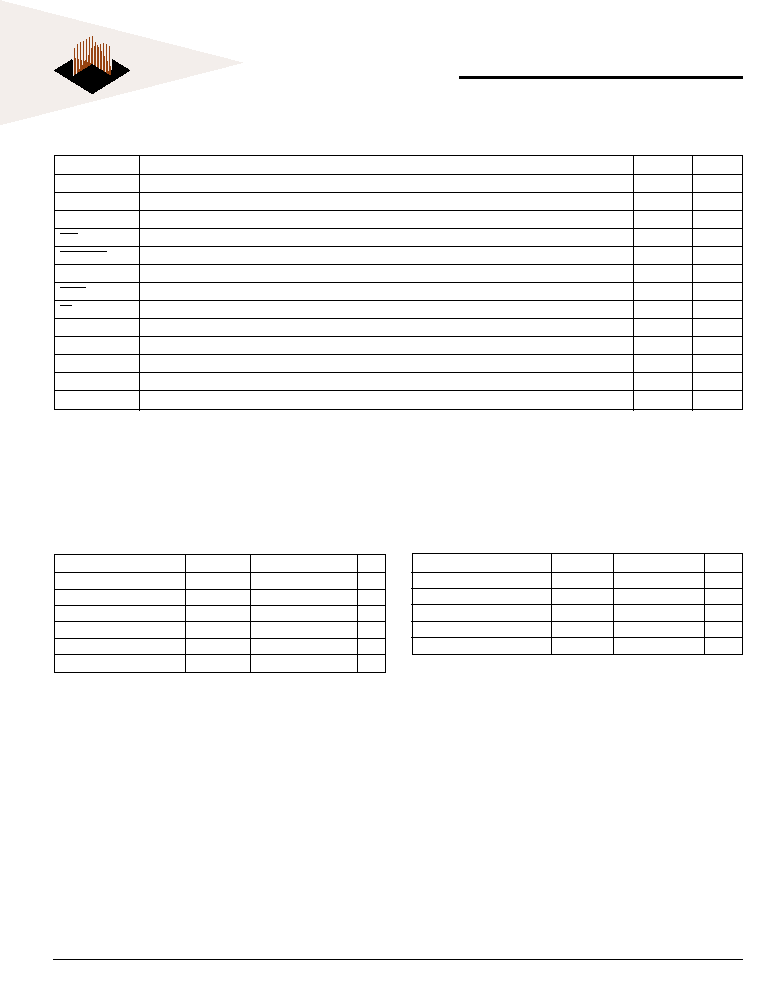
L2 CACHE CONTROL REGISTER (L2CR)
The L2 cache control register, shown in Figure 5, is a supervisor-level, implementation-specific SPR used
to configure and operate the L2 cache. It is cleared by hard reset or power-on reset.
FIG. 5 L2 CACHE CONTROL REGISTER (L2CR)
The L2CR bits are described in Table 1.
L2E
L2SIZ
L2CLK
L2RAM
L2I
L2OH
0
0
0
0
0
0
0
0
0
0
0
0
0
0
1
2
3
4
6
7
8
9
10 11 12 13 14 15 16 17 18 19
30 31
L2WT
L2DF
L2PE
L2DR L2CTL L2TS
L2SL L2BYP
L2IP
Reserved
T
ABLE
1: L2CR B
IT
S
ETTINGS
Bit
Name
Function
0
L2E
L2 enable. Enables L2 cache operation (including snooping) starting with the next transaction the L2 cache unit receives. Before enabling the L2
cache, the L2 clock must be configured through L2CR[2CLK], and the L2 DLL must stabilize. All other L2CR bits must be set appropriately. The
L2 cache may need to be invalidated globally.
1
L2PE
L2 data parity generation and checking enable. Enables parity generation and checking for the L2 data RAM interface. When disabled, generated
parity is always zeros. L2 Parity is supported by WEDC's WED3C750A8M-200BX, but is dependent on application.
23
L2SIZ
L2 sizeShould be set according to the size of the L2 data RAMs used.
11
1 Mbyte - Setting for WED3C750A8M-200BX
46
L2CLK
L2 clock ratio (core-to-L2 frequency divider). Specifies the clock divider ratio based from the core clock frequency that the L2 data RAM interface
is to operate at. When these bits are cleared, the L2 clock is stopped and the on-chip DLL for the L2 interface is disabled. For nonzero values,
the processor generates the L2 clock and the on-chip DLL is enabled. After the L2 clock ratio is chosen, the DLL must stabilize before the L2
interface can be enabled. The resulting L2 clock frequency cannot be slower than the clock frequency of the 60x bus interface.
000
L2 clock and DLL disabled
001
˜1
010
˜1.5
011
Reserved
100
˜2 - Setting for WED3C750A8M-200BX
101
˜2.5
110
˜3
111
Reserved
8
White Electronic Designs Corporation Phoenix AZ (602) 437-1520
WED3C750A8M-200BX
White Electronic Designs
Bit
Name
Function
78
L2RAM
L2 RAM typeConfigures the L2 RAM interface for the type of synchronous SRAMs used:
Pipelined (register-register) synchronous burst SRAMs that clock addresses in and clock data out
The 750 does not burst data into the L2 cache, it generates an address for each access.
10 Pipelined (register-register) synchronous burst SRAM - Setting for WED3C750A8M-200BX
9
L2DO
L2 data-only. Setting this bit enables data-only operation in the L2 cache. For this operation, only transactions from the L1 data cache can be
cached in the L2 cache, which treats all transactions from the L1 instruction cache as cache-inhibited (bypass L2 cache, no L2 checking done).
L2 Data-only depends on application.
10
L2I
L2 global invalidate. Setting L2I invalidates the L2 cache globally by clearing the L2 bits including status bits. This bit must not be set while the
L2 cache is enabled. See Motorola's User manual for L2 Invalidation procedure.
11
L2CTL
L2 RAM control (ZZ enable). Setting L2CTL enables the automatic operation of the L2ZZ (low-power mode) signal for cache RAMs.
Sleep mode is supported by the WED3C750A8M-200BX. While L2CTL is asserted, L2ZZ asserts automatically when the device enters nap or
sleep mode and negates automatically when the device exits nap or sleep mode. This bit should not be set when the device is in nap mode and
snooping is to be performed through deassertion of QACK.
12
L2WT
L2 write-through. Setting L2WT selects write-through mode (rather than the default write-back mode) so all writes to the L2 cache also write
through to the 60x bus. For these writes, the L2 cache entry is always marked as clean (valid unmodified) rather than dirty (valid modified). This
bit must never be asserted after the L2 cache has been enabled as previously-modified lines can get remarked
as clean during normal operation.
13
L2TS
L2 test support. Setting L2TS causes cache block pushes from the L1 data cache that result from dcbf and dcbst instructions to be written only
into the L2 cache and marked valid, rather than being written only to the 60x bus and marked invalid in the L2 cache in case of hit. This bit
allows a dcbz/dcbf instruction sequence to be used with the L1 cache enabled to easily initialize the L2 cache with any address and data
information. This bit also keeps dcbz instructions from being broadcast on the 60x and single-beat cacheable store misses in the L2 from being
written to the 60x bus.
0: Setting for the L2 Test Support as this bit is reserved for tests.
1415
L2OH
L2 output hold. These bits configure output hold time for address, data, and control signals driven to the L2 data RAMs.
00 0.5 ns - Setting for WED3C750A8M-200BX
16
L2SL
L2 DLL slow. Setting L2SL increases the delay of each tap of the DLL delay line. It is intended to increase the delay through the DLL to
accommodate slower L2 RAM bus frequencies.
1: Setting for WED3C750A8M-200BX because L2 RAM interface is operated below 110 MHz.
17
L2DF
L2 differential clock. This mode supports the differential clock requirements of late-write SRAMs.
0: Setting for WED3C750A8M-200BX' because late-write SRAMs are not used.
18
L2BYP
L2 DLL bypass is reserved.
0: Setting for WED3C750A8M-200BX
1930
Reserved. These bits are implemented but not used; keep at 0 for future compatibility.
31
L2IP
L2 global invalidate in progress (read only)See the Motorola user's manual for L2 Invalidation procedure.
T
ABLE
1:L2CR B
IT
S
ETTINGS
(
CONTINUED
)
9
White Electronic Designs Corporation (602) 437-1520 www.whiteedc.com
WED3C750A8M-200BX
White Electronic Designs
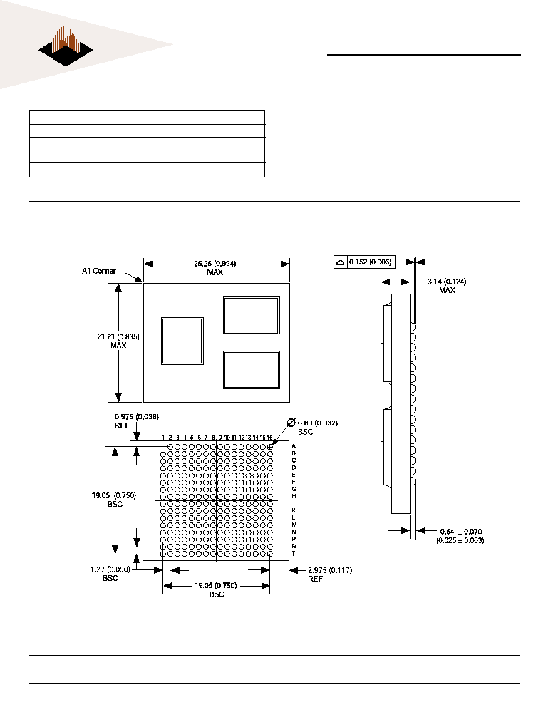
PACKAGE DIMENSIONS 255 BALL GRID ARRAY
P
ACKAGE
D
ESCRIPTION
Package Outline
21x25mm
Interconnects
255 (16x16 ball array less one)
Pitch
1.27mm
Maximum module height
3.90mm
Ball diameter
0.8mm
NOTES:
1. Dimensions in millimeters and paranthetically in inches.
2. A1 corner is designated with a ball missing the array.
10
White Electronic Designs Corporation Phoenix AZ (602) 437-1520
WED3C750A8M-200BX
White Electronic Designs
NOT
RECOMMENDED
FOR
NEW
DESIGNS*
DEVICE GRADE:
I = Industrial
-40∞C to +85∞C
M = Military Screened
-55∞C to +125∞C
PACKAGE TYPE:
B = 255 Ceramic Ball Grid Array
C = 255 Ceramic Column Grid Array*
CORE FREQUENCY (MHz)
L2 CACHE DENSITY:
8Mbits = 128K x 72 SSRAM
PowerPC:
Type 750A
C = MCM-C
3 = PowerPC
WHITE ELECTRONIC DESIGNS CORP.
O
RDERING
I
NFORMATION
WED 3 C 750A 8M 200 X X
PowerPC is a trademark of International Business Machine Corp.
* Advanced Package, contact factory for availability.
** This data sheet describes a product that is not recommended
for new designs.