WED3C755E8M-XBX
1
White Electronic Designs Corporation ∑ (602) 437-1520 ∑ www.wedc.com
White Electronic Designs
White Electronic Designs Corp. reserves the right to change products or specifi cations without notice.
May, 2003
Rev 2
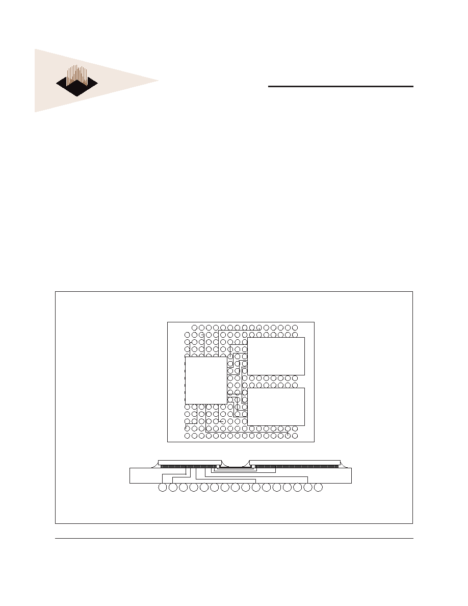
RISC MICROPROCESSOR MULTI-CHIP PACKAGE
OVERVIEW
The WEDC 755E/SSRAM multichip package is targeted
for high performance, space sensitive, low power systems
and supports the following power management features:
doze, nap, sleep and dynamic power management. The
WED3C755E8M-XBX multichip package consists of:
755 RISC processor (E die revision)
Dedicated 1MB SSRAM L2 cache, confi gured as
128Kx72
21mmx25mm, 255 Ceramic Ball Grid Array (CBGA)
Core Frequency/L2 Cache Frequency (300MHz/
150MHz, 350MHz/175MHz)
Maximum 60x Bus frequency = 66MHz
FIG. 1 - MULTI-CHIP PACKAGE DIAGRAM
µP
755E
SSRAM
SSRAM
FEATURES
The WED3C755E8M-XBX is offered in Commercial
(0∞C to +70∞C), industrial (-40∞C to +85∞C) and military
(-55∞C to +125∞C) temperature ranges and is well suited
for embedded applications such as missiles, aerospace,
fl ight computers, fi re control systems and rugged critical
systems.
Footprint compatible with WED3C7558M-XBX and
WED3C750A8M-200BX
Footprint compatible with Motorola MPC 745
This product is subject to change without notice.
WED3C755E8M-XBX
2
White Electronic Designs Corporation ∑ (602) 437-1520 ∑ www.wedc.com
White Electronic Designs
White Electronic Designs Corp. reserves the right to change products or specifi cations without notice.
May, 2003
Rev 2
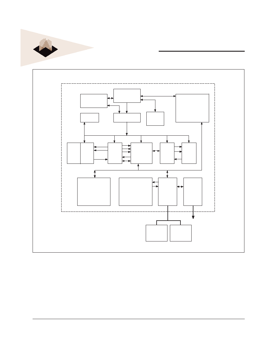
Completion
Control Unit
32K ICache
32K DCache
FXU1
L2Tags
SSRAM
SSRAM
60x Bus
L2 Cache
BIU
L2 Cache
Bus
60x BIU
FPU
FPRs
LSU
Rename
Buffers
Rename
Buffers
GPRs
FXU2
System Unit
Dispatch
BHT/BTIC
Instruction
Fetch
Branch Unit
FIG. 2 - BLOCK DIAGRAM
WED3C755E8M-XBX
3
White Electronic Designs Corporation ∑ (602) 437-1520 ∑ www.wedc.com
White Electronic Designs
White Electronic Designs Corp. reserves the right to change products or specifi cations without notice.
May, 2003
Rev 2
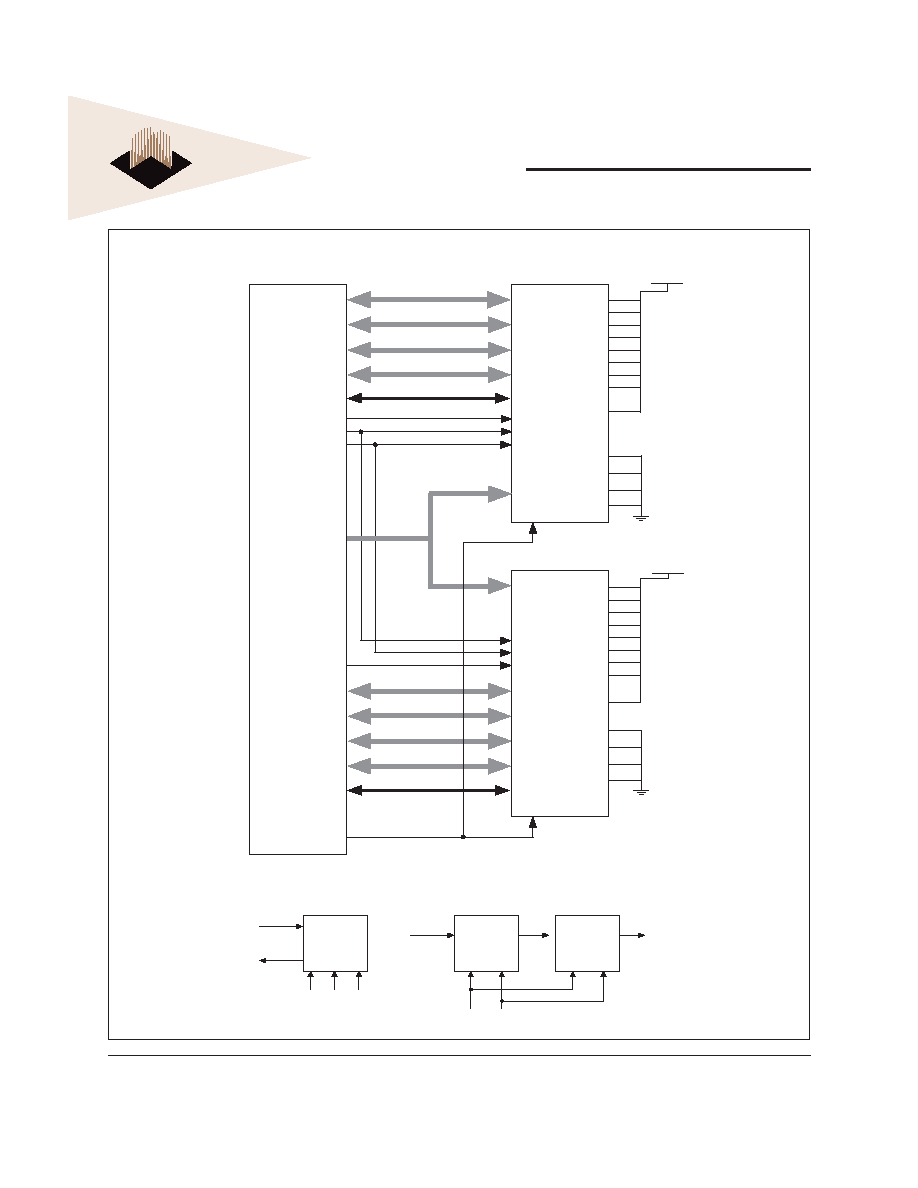
FIG. 3 - BLOCK DIAGRAM, L2 INTERCONNECT
L2pin_DATA
L2pin_DATA
L2pin_DATA
L2pin_DATA
L2 CLK_OUT A
L2WE#
L2CE#
A0-16
L2CLK_OUT B
L2pin_DATA
L2pin_DATA
L2pin_DATA
L2pin_ DATA
L2ZZ
mP
755
DQa
DQb
DQc
DQd
K
SGW#
SE1#
SA0-16
SA0-16
SGW#
SE1#
K
DQa
DQb
DQc
DQd
SSRAM 1
SSRAM 2
FT#
SBd#
SBc
SBb#
SBa#
SW#
ADSP#
ADV#
SE2
ADSC#
SE3#
LBO#
G#
FT#
SBd#
SBc#
SBb#
SBa#
SW#
ADSP#
ADV#
SE2
ADSC#
SE3#
LBO#
G#
L20Vdd
L20Vdd
L2DP0-3
DP0-3
L2DP4-7
DP0-3
ZZ
ZZ
U2
U1
E
#
FIG. 4. - BLOCK DIAGRAM, L2 INTERCONNECT
L2 Cache
SSRAM
U2
L2 Cache
SSRAM
U1
STDO
STDI
STMS STCK
TDI
TDO
755 E
TMS TCK TRST
WED3C755E8M-XBX
4
White Electronic Designs Corporation ∑ (602) 437-1520 ∑ www.wedc.com
White Electronic Designs
White Electronic Designs Corp. reserves the right to change products or specifi cations without notice.
May, 2003
Rev 2
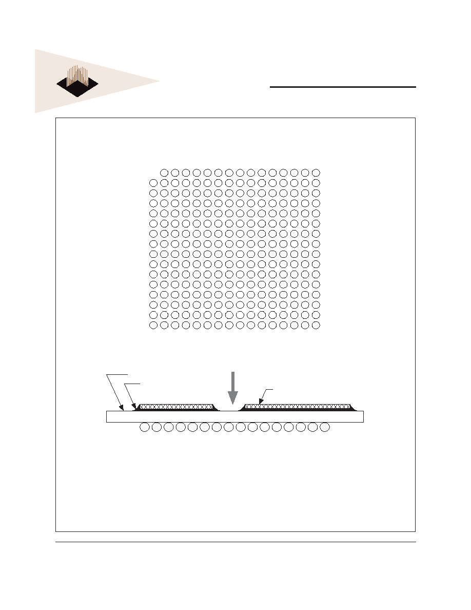
FIG. 5 - PIN ASSIGNMENTS
Ball assignments of the 255 CBGA package as viewed from the top surface.
A
B
C
D
E
F
G
H
J
K
L
M
N
P
R
T
1
2
3 4 5 6 7 8 9 10 11 12 13 14 15 16
Underfill Encapsulant
View
Die
Substrate Assembly
Side profi le of the CBGA package to indicate the direction of the top surface view.
WED3C755E8M-XBX
5
White Electronic Designs Corporation ∑ (602) 437-1520 ∑ www.wedc.com
White Electronic Designs
White Electronic Designs Corp. reserves the right to change products or specifi cations without notice.
May, 2003
Rev 2
PACKAGE PINOUT LISTING
Signal Name
Pin Number
Active
I/O
I/F Voltage
A[0-31]
C16, E4, D13, F2, D14, G1, D15, E2, D16, D4, E13, G2, E15, H1, E16, H2, F13, J1,
F14, J2, F15, H3, F16, F4, G13, K1, G15, K2, H16, M1, J15, P1
High
I/O
OV
CC
AACK#
L2
Low
Input
OV
CC
ABB#
K4
Low
I/O
OV
CC
AP[0-3]
C1, B4, B3, B2
High
I/O
OV
CC
ARTRY#
J4
Low
I/O
OV
CC
AV
CC
A10
--
--
2.0V
BG#
L1
Low
Input
OV
CC
BR#
B6
Low
Output
OV
CC
BVSEL (4, 5, 6)
B1
High
Input
OV
CC
CI#
E1
Low
Output
OV
CC
CKSTP_IN#
D8
Low
Input
OV
CC
CKSTP_OUT#
A6
Low
Ouput
OV
CC
CLK_OUT
D7
-- Output
OV
CC
DBB#
J14
Low
I/O
OV
CC
DBG#
N1
Low
Input
OV
CC
DBDIS#
H15
Low
Input
OV
CC
DBWO#
G4
Low
Input
OV
CC
DH[0-31]
P14, T16, R15, T15, R13, R12, P11, N11, R11, T12, T11, R10, P9, N9, T10, R9, T9, P8,
N8, R8, T8, N7, R7, T7, P6, N6, R6, T6, R5, N5, T5, T4
High
I/O
OV
CC
DL[0-31]
K13, K15, K16, L16, L15, L13, L14, M16, M15, M13, N16, N15, N13, N14, P16, P15,
R16, R14, T14, N10, P13, N12, T13, P3, N3, N4, R3, T1, T2, P4, T3, R4
High
I/O
OV
CC
DP[0-7]
M2, L3, N2, L4, R1, P2, M4, R2
High
I/O
OV
CC
DRTRY#
G16
Low
Input
OV
CC
GBL#
F1
Low
I/O
OV
CC
GND
C5, C12, E3, E6, E8, E9, E11, E14, F5, F7, F10, F12, G6, G8, G9, G11, H5, H7, H10,
H12, J5, J7, J10, J12, K6, K8, K9, K11, L5, L7, L10, L12, M3, M6, M8, M9, M11, M14,
P5, P12
--
--
GND
HRESET#
A7
Low
Input
OV
CC
INT#
B15
Low
Input
OV
CC
L1_TSTCLK (1)
D11
High
Input
--
L2_TSTCLK (1)
D12
High
Input
--
L2AV
CC
(8)
L11
--
--
2.0V
L2OV
CC
E10, E12, M12, G12, G14, K12, K14
--
--
L20V
CC
L2VSEL (4, 5, 6, 7)
B5
High
Input
L20V
CC
LSSD_MODE# (1)
B10
Low
Input
--
MCP#
C13
Low
Input
OV
CC
NC (No-connect)
C3, C6, D5, D6, H4, A4, A5, A2, A3
--
--
--
OVCC (2)
C7, E5, G3, G5, K3, K5, P7, P10, E7, M5, M7, M10
--
--
OV
CC
PLL_CFG[0-3]
A8, B9, A9, D9
High
Input
OV
CC
QACK#
D3
Low
Input
OV
CC
QREQ#
J3
Low
Output
OV
CC
RSRV#
D1
Low
Output
OV
CC
SMI#
A16
Low
Input
OV
CC
SRESET#
B14
Low
Input
OV
CC
STCK (9)
B7
--
Input
L20V
CC
STDI
C8
--
Input
L20V
CC
STDO
J16
--
Output
L20V
CC
WED3C755E8M-XBX
6
White Electronic Designs Corporation ∑ (602) 437-1520 ∑ www.wedc.com
White Electronic Designs
White Electronic Designs Corp. reserves the right to change products or specifi cations without notice.
May, 2003
Rev 2
Signal Name
Pin Number
Active
I/O
I/F Voltage (7)
STMS (10)
B8
--
Input
L2OV
CC
SYSCLK
C9
--
Input
OV
CC
TA#
H14
Low
Input
OV
CC
TBEN
C2
High
Input
OV
CC
TBST#
A14
Low
I/O
OV
CC
TCK
C11
High
Input
OV
CC
TDI (6)
A11
High
Input
OV
CC
TDO
A12
High
Output
OV
CC
TEA#
H13
Low
Input
OV
CC
TLBISYNC#
C4
Low
Input
OV
CC
TMS (6)
B11
High
Input
OV
CC
TRST# (6)
C10
Low
Input
OV
CC
TS#
J13
Low
I/O
OV
CC
TSIZ[0-2]
A13, D10, B12
High
Output
OV
CC
TT[0-4]
B13, A15, B16, C14, C15
High
I/O
OV
CC
WT
D2
Low
Output
OV
CC
V
CC
(2)
F6, F8, F9, F11, G7, G10, H6, H8, H9, H11, J6, J8, J9, J11, K7, K10, L6, L8, L9
--
--
2.0V
VOLDET (3)
F3
--
Output
--
PACKAGE PINOUT LISTING (continued)
NOTES:
1.
These are test signals for factory use only and must be pulled up to OV
CC
for
normal machine operation.
2. OV
CC
inputs supply power to the I/O drivers and V
CC
inputs supply power to the
processor core.
3.
Internally tied to GND in the BGA package to indicate to the power supply that a
low-voltage processor is present. This signal is not a power supply pin.
4.
To allow processor bus I/0 voltage changes, provide the option to connect BVSEL
and L2VSEL independently to either OV
CC
or to GND .
5.
Uses one of 15 existing no-connects in WEDC's WED3C750A8M-200BX.
6.
Internal pull up on die.
7. OV
CC
supplies power to the processor bus, JTAG, and all control signals except
the L2 cache controls (L2CE, L2WE, and L2ZZ); L2OV
CC
supplies power to
the L2 cache I/O interface (L2ADDR (0-16], L2DATA (0-63), L2DP{0-7] and
L2SYNC-OUT) and the L2 control signals and the SSRAM power supplies; and
V
CC
supplies power to the processor core and the PLL and DLL (after fi ltering to
become AVCC and L2AV
CC
respectively). This column serves as a reference for
the nominal voltage supported on a given signal as selected by the BVSEL/
L2VSEL pin confi gurations and the voltage supplied. For actual recommended
value of V
IN
or supply voltages see Recommended Operating Conditions Table.
8.
Uses one of 20 existing V
CC
pins in WEDC's WED3C750A8M-200BX, no board
level design changes are necessary. For new designs of WED3C755E8M-XBX
refer to PLL power supply fi ltering.
9.
To disable SSRAM TAP controllers without interfering with the normal operation
of the devices, STCK should be tied low (GND) to prevent clocking the devices.
10.
STDI and STMS are internally pulled up and may be left unconnected. Upon
power-up the SSRAM devices will come up in a reset state which will not interfere
with the operation of the device.

WED3C755E8M-XBX
7
White Electronic Designs Corporation ∑ (602) 437-1520 ∑ www.wedc.com
White Electronic Designs
White Electronic Designs Corp. reserves the right to change products or specifi cations without notice.
May, 2003
Rev 2
Characteristic
Symbol
Value
Unit
Notes
Core supply voltage
V
CC
-0.3 to 2.5
V
(4)
PLL supply voltage
AV
CC
-0.3 to 2.5
V
(4)
L2 DLL supply voltage
L2AV
CC
-0.3 to 2.5
V
(4)
60x bus supply voltage
OV
CC
-0.3 to 3.6
V
(3)
L2 bus supply voltage
L2OV
CC
-0.3 to 3.6
V
(3)
Input supply
Processor Bus
V
IN
-0.3 to 0V
CC
+0.3
V
(2)
L2 bus
V
IN
-0.3 to L20V
CC
+0.3
V
(2)
JTAG Signals
V
IN
-0.3 to 3.6
V
(2)
Storage temperature range
Tstg
-55 to 150
∞C
ABSOLUTE MAXIMUM RATINGS
Characteristic
Symbol
Recommended Value
Unit
Core supply voltage
V
CC
2.0 ± 100mV
V
PLL supply voltage
AV
CC
2.0 ± 100mV
V
L2 DLL supply voltage
L2AV
CC
2.0 ± 100mV
V
P r o c e s s o r b u s s u p p l y
voltage
(2)
BVSEL = 1
OV
CC
2.5± 125mV
V
3.3 ± 165mV
V
L2 bus supply voltage
(3)
L2VSEL = 1
L20V
CC
3.3 ± 165mV
V
Input Voltage
Processor bus
V
IN
GND to OV
CC
V
JTAG Signals
V
IN
GND to OV
CC
V
NOTES:
1.
Functional and tested operating conditions are given in Operating Conditions
table. Absolute maximum ratings are stress ratings only, and functional operation
at the maximums is not guaranteed. Stresses beyond those listed may affect
device reliability or cause permanent damage to the device.
2.
Caution: V
IN
must not exceed OV
CC
by more than 0.3V at any time including
during power-on reset.
3.
Caution: OV
CC
/L2OV
CC
must not exceed V
CC
/AV
CC
/L2AV
CC
by more than 1.6 V
at any time including during power-on reset.
4.
Caution: V
CC
/AV
CC
/L2AV
CC
must not exceed L2OV
CC
/OV
CC
by more than 0.4 V
at any time including during power-on reset.
RECOMMENDED OPERATING CONDITIONS (1)
NOTE:
1.
These are the recommended and tested operating conditions. Proper device
operation outside of these conditions is not guaranteed
2.
BVSEL = 0 is not available
3.
L2VSEL = 0 is not available

WED3C755E8M-XBX
8
White Electronic Designs Corporation ∑ (602) 437-1520 ∑ www.wedc.com
White Electronic Designs
White Electronic Designs Corp. reserves the right to change products or specifi cations without notice.
May, 2003
Rev 2
Processor (CPU) Frequency/L2 Fre-
quency
Unit
Notes
300/150 MHz
350/175MHz
Full-on Mode
Typical
Maximum
4.1
4.6
W
1, 3
6.7
7.9
W
1, 2
Doze Mode
Maximum
2.5
2.8
W
1, 2
Nap Mode
Maximum
1700
1800
mW
1, 2
Sleep Mode
Maximum
1200
1300
mW
1, 2
Sleep Mode≠PLL and DLL Disabled
Maximum
500
500
mW
1, 2
POWER CONSUMTION
V
CC
=AV
CC
=2.0±0.1V, OV
CC
=3.3V ±5% V
DC
, GND=0 V
DC
, 0Tj<105∞C
NOTES:
1.
These values apply for all valid 60x bus and L2 bus ratios. The values do
not include OV
CC
; AV
CC
and L2AV
CC
suppling power. OV
CC
power is system
dependent, but is typically <10% of V
CC
power. Worst case power consumption,
for AV
CC
=15mW and L2AV
CC
=15mW.
2.
Maximum power is measured at V
CC
=2.1V while running an entirely cache-
resident, contrived sequence of instructions which keep the execution units
maximally busy.
3.
Typical power is an average value measured at V
CC
=AV
CC
=L2AV
CC
=2.0V,
OV
CC
=L2OV
CC
=3.3V in a system, executing typical applications and benchmark
sequences.
L2 CACHE CONTROL REGISTER (L2CR)
The L2 cache control register, shown in Figure 5, is a supervisor-level, implementation-specifi c SPR used to confi gure
and operate the L2 cache. It is cleared by hard reset or power-on reset.
The L2CR bits are described in Table 1.
FIG. 5 - L2 CACHE CONTROL REGISTER (L2CR)
Description
Symbol
PPC
SSRAM
Units
Notes
Junction to Ambient (No Airfl ow)
Theta JA
14.2
11.2
C/W
1
Junction to Ball
Theta JB
8.6
5.7
C/W
1
Junction to Case (Top)
Theta JC
0.1
0.1
C/W
1
NOTE 1: Refer to PBGA Thermal Resistance Correlation at www.whiteedc.com in the application notes section for modeling conditions
BGA THERMAL RESISTANCE
0
1 2
3 4
6 7
8
9
10 11 12 13 14
15 16 17
18
19
20
21
22 23
24
31
30
L2E
L2PE
L2SIZ
L2CLK
L2RAM
L2DO
L2I
L20H
L2CTL L2WT L2TS
L2SL
L2DF
L2BYP
L2IO
L2CS
L2DRO
L2CTR
L2IP
0
0
Reserved
WED3C755E8M-XBX
9
White Electronic Designs Corporation ∑ (602) 437-1520 ∑ www.wedc.com
White Electronic Designs
White Electronic Designs Corp. reserves the right to change products or specifi cations without notice.
May, 2003
Rev 2
TABLE 1 - L2CR BIT SETTINGS
Bit
Name
Function
0
L2E
L2 enable. Enables L2 cache operation (including snooping) starting with the next transaction the L2 cache unit receives. Before
enabling the L2 cache, the L2 clock must be confi gured through L2CR[2CLK], and the L2 DLL must stabilize. All other L2CR bits
must be set appropriately. The L2 cache may need to be invalidated globally.
1
L2PE
L2 data parity checking enable. Enables parity generation and checking for the L2 data RAM interface. When disabled, gener-
ated parity is always zeros. L2 Parity is supported by WEDC's WED3C755E8M-XBX, but is dependent on application.
2≠3
L2SIZ
L2 size--Should be set according to the size of the L2 data RAMs used.
11 1 Mbyte - Setting for WED3C755E8M-XBX
4≠6
L2CLK
L2 clock ratio (core-to-L2 frequency divider). Specifi es the clock divider ratio based from the core clock frequency that the L2
data RAM interface is to operate at. When these bits are cleared, the L2 clock is stopped and the on-chip DLL for the L2 interface
is disabled. For nonzero values, the processor generates the L2 clock and the on-chip DLL is enabled. After the L2 clock ratio is
chosen, the DLL must stabilize before the L2 interface can be enabled. The resulting L2 clock frequency cannot be slower than
the clock frequency of the 60x bus interface.
000 L2 clock and DLL disabled
001 ˜ 1
010 ˜ 1.5
011 Reserved
100 ˜ 2
101 ˜ 2.5
110 ˜ 3
111 Reserved
7≠8
L2RAM
L2 RAM type--Confi gures the L2 RAM interface for the type of synchronous SRAMs used:
∑ Pipelined (register-register) synchronous burst SRAMs that clock addresses in and clock data out.
The 755 does not burst data into the L2 cache, it generates an address for each access.
10 Pipelined (register-register) synchronous burst SRAM - Setting for WED3C755E8M-XBX
9
L2DO
L2 data only. Setting this bit enables data-only operation in the L2 cache. For this operation, instruction transactions from the L1
Instruction cache already cached in the L2 cache can hit in the L2, but new instruction transactions from the L1 instruction cache
are treated as cache-inhibited (bypass L2 cache, no L2 checking done). When both L2DO adn L2IO are set, the L2 cache is ef-
fectively locked (cache misses do not cause new entries to be allocated but write hits use the L2).
10
L2I
L2 global invalidate. Setting L2I invalidates the L2 cache globally by clearing the L2 status bits. This bit must not be set while the
L2 cache is enabled. See Motorola's User manual for L2 Invalidation procedure.
11
L2CTL
L2 RAM control (ZZ enable). Setting L2CTL enables the automatic operation of the L2ZZ (low-power mode) signal for cache
RAMs. Sleep mode is supported by the WED3C755E8M-XBX. While L2CTL is asserted, L2ZZ asserts automatically when the
device enters nap or sleep mode and negates automatically when the device exits nap or sleep mode. This bit should not be set
when the device is in nap mode and snooping is to be performed through deassertion of QACK#.
12
L2WT
L2 write-through. Setting L2WT selects write-through mode (rather than the default write-back mode) so all writes to the L2 cache
also write through to the system bus. For these writes, the L2 cache entry is always marked as exclusive rather than modifi ed.
This bit must never be asserted after the L2 cache has been enabled as previously-modifi ed lines can get remarked as exclusive
during normal operation.
13
L2TS
L2 test support. Setting L2TS causes cache block pushes from the L1 data cache that result from dcbf and dcbst instructions to
be written only into the L2 cache and marked valid, rather than being written only to the system bus and marked invalid in the L2
cache in case of hit. This bit allows a dcbz/dcbf instruction sequence to be used with the L1 cache enabled to easily initialize the
L2 cache with any address and data information. This bit also keeps dcbz instructions from being broadcast on the system and
single-beat cacheable store misses in the L2 from being written to the system bus.
0: Setting for the L2 Test support as this bit is reserved for tests.
14≠15 L2OH
L2 output hold. These bits confi gure output hold time for address, data, and control signals driven to the L2 data RAMs.
00: Least Hold Time - Setting for WED3C755E8M-XBX
WED3C755E8M-XBX
10
White Electronic Designs Corporation ∑ (602) 437-1520 ∑ www.wedc.com
White Electronic Designs
White Electronic Designs Corp. reserves the right to change products or specifi cations without notice.
May, 2003
Rev 2
Bit
Name
Function
16
L2SL
L2 DLL slow. Setting L2SL increases the delay of each tap of the DLL delay line. It is intended to increase the delay through the
DLL to accommodate slower L2 RAM bus frequencies.
0: Setting for WED3C755E8M-XBX because L2 RAM interface is operated above 100 MHz.
17
L2DF
L2 differential clock. This mode supports the differential clock requirements of late-write SRAMs.
0: Setting for WED3C755E8M-XBX because late-write SRAMs are not used.
18
L2BYP
L2 DLL bypass is reserved.
0: Setting for WED3C755E8M-XBX
19-20
--
Reserved. These bits are implemented but not used; keep at 0 for future compatibility.
21
L2IO
L2 Instruction-only. Setting this bit enables instruction-only operation in the L2 cache. For this operation, data transactions from
the L1 data cache already cached in the L2 cache can hit in the L2 (including writes), but new data transactions (transactions
that miss in the L2) from the L1 data cashe are treated as cache-inhibited (bypass L2 cache, no L2 checking done). When both
L2DO and L2IO are set, the L2 cache is effectively locked (cache misses do not cause new entries to be allocated but write hits
use the L2). Note that this bit can be programmed dynamically.
22
L2CS
L2 Clock Stop. Setting this bit causes the L2 clocks to the SRAMs to automatically stop whenever the MPC755 enters nap or
sleep modes, and automatically restart when exiting those modes (including for snooping during nap mode). It operates by
asynchronously gating off the
L2CLK_OUT [A:B] signals while in nap or sleep mode. The L2SYNC_OUT/SYNC_IN path
remains in operation, keeping the DLL synchronized. This bit is provided as a power-saving alternative to the L2CTL bit and its
corresponding ZZ pin, which may not be useful for dynamic stopping/restarting of the L2 interface from nap and sleep modes
due to the relatively long recovery time from ZZ negation that the SRAM requires.
23
L2DRO
L2 DLL rollover. Setting this bit enables a potential rollover (or actual rollover) condition of the DLL to cause a checkstop for the
processor. A potential rollover condition occurs when the DLL is selecting the last tap of the delay line, and thus may risk rolling
over to the fi rst tap with one adjustment while in the process of keeping synchronized. Such a condition is improper operation
for the DLL, and, while this condition is not expected, it allows detection for added security. This bit can be set when the DLL is
fi rst enabled (set with the L2CLK bits) to detect rollover during initial synchronization. It could also be set when the L2 cache is
enabled (with L2E bit) after the DLL has achieved its initial lock.
24≠30
L2CTR
L2 DLL counter (read-only). These bits indicate the current value of the DLL counter (0 to 127). They are asynchronously read
when the L2CR is read, and as such should be read at least twice with the same value in case the value is asynchronously
caught in transition. These bits are intended to provide observability of where in the 128-bit delay chain the DLL is at any given
time. Generally, the DLL operation should be considered at risk if it is found to be within a couple of taps of its beginning or end
point (tap 0 or tap 128).
31
L2IP
L2 global invalidate in progress (read only)--See the Motorola user's manual for L2 Invalidation procedure.
TABLE 1 - L2CR BIT SETTINGS
WED3C755E8M-XBX
11
White Electronic Designs Corporation ∑ (602) 437-1520 ∑ www.wedc.com
White Electronic Designs
White Electronic Designs Corp. reserves the right to change products or specifi cations without notice.
May, 2003
Rev 2
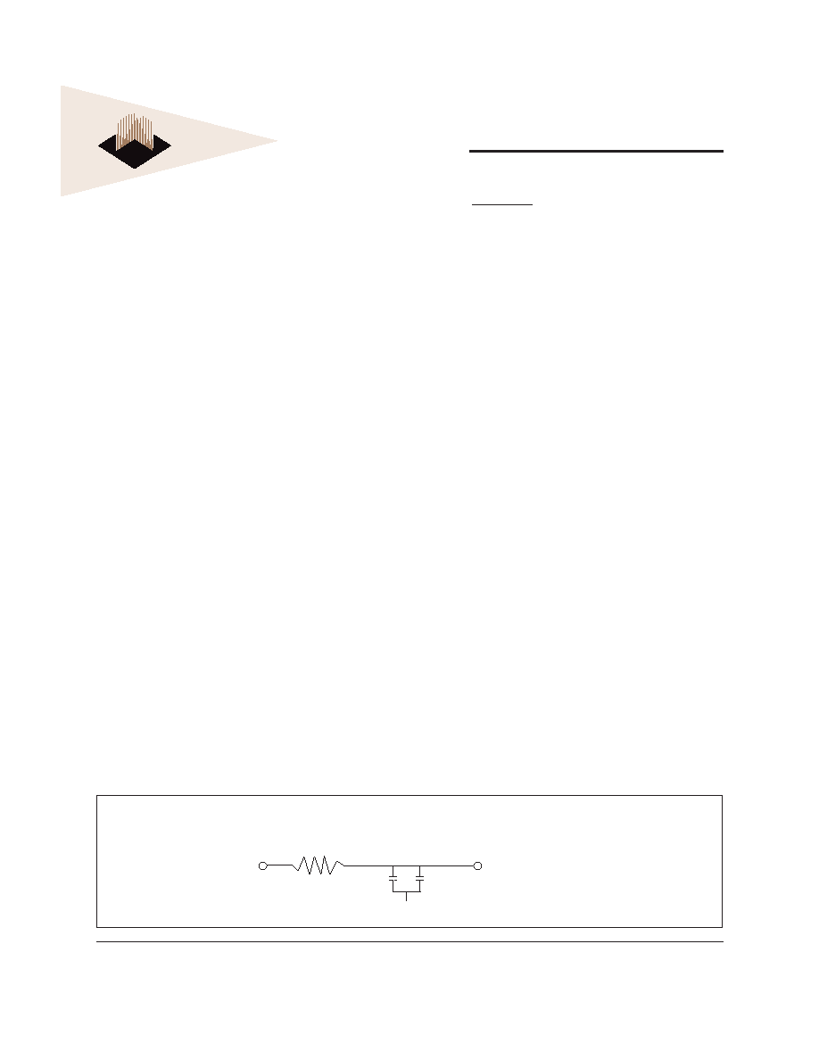
FIG. 6 - POWER SUPPLY FILTER CIRCUIT
PLL POWER SUPPLY FILTERING
The AV
CC
and L2AV
CC
power signals are provided on
the WED3C755E8M-XBX to provide power to the clock
generation phase-locked loop and L2 cache delay-locked
loop respectively. To ensure stability of the internal clock,
the power supplied to the AV
CC
input signal should be
fi ltered of any noise in the 500kHz to 10 MHz resonant
frequency range of the PLL. A circuit similar to the
one shown in Figure 6 using surface mount capacitors
with minimum Effective Series Inductance (ESL) is
recommended. Multiple small capacitors of equal value
are recommended over a single large value capacitor.
The circuit should be placed as close as possible to the
AV
CC
pin to minimize noise coupled from nearby circuits.
An identical but separate circuit should be placed as close
as possible to the L2AV
CC
pin. It is often possible to route
directly from the capacitors to the AV
CC
pin, which is on the
periphery of the 255 BGA footprint, without the inductance
of vias. The L2AV
CC
pin may be more diffi cult to route but
is proportionately less critical.
PULL-UP RESISTOR REQUIREMENTS
The WED3C755E8M-XBX requires pull-up resistors (1
kW-5 kW) on several control pins of the bus interface to
maintain the control signals in the negated state after they
have been actively negated and released by the processor
or other bus masters. These pins are TS#, ABB#, AACK#,
ARTRY#, DBB#, DBWO#, TA#, TEA#, and DBDIS#.
DRTRY# should also be connected to a pull-up resistor
(1 kW-5 kW) if it will be used by the system; otherwise,
this signal should be connected to HRESET# to select
NO-DRTRY mode.
Three test pins also require pull-up resistors (100 W-1 kW).
These pins are L1_TSTCLK, L2_TSTCLK, and LSSD_
MODE#. These signals are for factory use only and must
be pulled up to OV
CC
for normal machine operation.
In addition, CKSTP_OUT# is an open-drain style output
that requires a pull-up resistor (1 kW-5 kW) if it is used by
the system. During inactive periods on the bus, the address
and transfer attributes may not be driven by any master
and may, therefore, fl oat in the high-impedance state for
relatively long periods of time. Since the processor must
continually monitor these signals for snooping, this fl oat
condition may cause additional power draw by the input
receivers on the processor or by other receivers in the
system. These signals can be pulled up through weak (10
kW) pull-up resistors by the system or may be otherwise
driven by the system during inactive periods of the bus to
avoid this additional power draw, but address bus pull-up
resistors are not neccessary for proper device operation.
The snooped address and transfer attribute inputs are:
A[0:31], AP[0:3], TT[0:4], TBST#, and GBL#.
The data bus input receivers are normally turned off
when no read operation is in progress and, therefore, do
not require pull-up resistors on the bus. Other data bus
receivers in the system, however, may require pull-ups, or
that those signals be otherwise driven by the system during
inactive periods by the system. The data bus signals are:
DH[0:31], DL[0:31], and DP[0:7].
If 32-bit data bus mode is selected, the input receivers of
the unused data and parity bits will be disabled, and their
outputs will drive logic zeros when they would otherwise
normally be driven. For this mode, these pins do not require
pull-up resistors, and should be left unconnected by the
system to minimize possible output switching.
If address or data parity is not used by the system, and
the respective parity checking is disabled through HID0,
the input receivers for those pins are disabled, and those
pins do not require pull-up resistors and should be left
unconnected by the system. If all parity generation is
disabled through HID0, then all parity checking should
also be disabled through HID0, and all parity pins may be
left unconnected by the system.
AV
CC
(or L2AV
CC
)
2.2
µF
2.2
µF
GND
Low ESL surface mount capacitors
V
CC
10

WED3C755E8M-XBX
12
White Electronic Designs Corporation ∑ (602) 437-1520 ∑ www.wedc.com
White Electronic Designs
White Electronic Designs Corp. reserves the right to change products or specifi cations without notice.
May, 2003
Rev 2
Package Outline
21x25mm
Interconnects
255 (16x16 ball array less one)
Pitch
1.27mm
Maximum module height
3.90mm
Ball diameter
0.8mm
PACKAGE DIMENSIONS 255 BALL GRID ARRAY
PACKAGE DESCRIPTION
NOTES:
1. Dimensions in millimeters and paranthetically in inches.
2. A1 corner is designated with a ball missing the array.
T
R
P
N
M
L
K
J
H
G
F
E
D
C
B
A
1 2 3 4 5 6 7 8 9 10 11
12 13 14 15
16
BOTTOM VIEW
TOP VIEW
A1 Corner
25.25 (0.094)
MAX
3.14 (0.024)
MAX
3.04 (0.119)
MAX
0.64 ± 0.070
(0.025 ± 0.003)
2.20 ± (0.087)
MAX
19.05 (0.750)
BSC
2.975 (0.117)
REF
21.21 (0.835)
MAX
19.05 (0.750)
BSC
0.975 (0.038)
REF
0.80 (0.032)
BSC
1.27 (0.050)
BSC
0.152 (0.006)

WED3C755E8M-XBX
13
White Electronic Designs Corporation ∑ (602) 437-1520 ∑ www.wedc.com
White Electronic Designs
White Electronic Designs Corp. reserves the right to change products or specifi cations without notice.
May, 2003
Rev 2
WED 3 C 755E 8M X B X
DEVICE GRADE:
M = Military Screened
-55∞C to +125∞C
I = Industrial
-40∞C to +85∞C
C = Commercial
0∞C to +70∞C
PACKAGE TYPE:
B = 255 Ceramic Ball Grid Array
CORE FREQUENCY (MHz)
350 = 350MHz/175MHz L2 cache
300 = 300MHz/150MHz L2 cache
L2 CACHE DENSITY:
8Mbits = 128K x 72 SSRAM
PowerPCTM:
Type 755E - 'E' Die Revision (2.8)
C = MULTICHIP PACKAGE
3 = PowerPCTM
WHITE ELECTRONIC DESIGNS CORP.
ORDERING INFORMATION
PowerPCTM is a trademark of International Business Machine Corp.

WED3C755E8M-XBX
14
White Electronic Designs Corporation ∑ (602) 437-1520 ∑ www.wedc.com
White Electronic Designs
White Electronic Designs Corp. reserves the right to change products or specifi cations without notice.
May, 2003
Rev 2
Document Title
PowerPC 755 + L2 Cache Multi-Chip Package
Revision History
Rev #
History
Release Date
Status
Rev 0
Initial Release
September 2002
Final
Rev 1
Changes (Pg. 1, 6, 7)
1.1 Remove 'Selects 3.3V interface' and 'Selects 2.0V interface from note 4 of pack-
age pinout listing.
1.2 Add notes 'BVSED = 0 is not available' and 'L2VSED = 0 is not available' to Rec-
ommended Operating Conditions Table
February 2003
Final
Rev 2
Changes (Pg. 1, 8, 14)
1.1 Add Thermal Resistance Table on page 8
1.2 Add Revision History as page 14
May 2003
Final