
1
White Electronic Designs Corporation (508) 485-4000 www.whiteedc.com
June 2003 Rev. 1
ECO #16373
WED3DG64128V-D1
White Electronic Designs Corp reserves the right to change products or specifications without notice.
1GB- 128Mx64 SDRAM, UNBUFFERED W/PLL
n PC100 and PC133 compatible
n Burst Mode Operation
n Auto and Self Refresh capability
n LVTTL compatible inputs and outputs
n Serial Presence Detect with EEPROM
n Fully synchronous: All signals are registered on the positive
edge of the system clock
n Programmable Burst Lengths: 1, 2, 4, 8 or Full Page
n 3.3 volt 6 0.3v Power Supply
n 144 Pin SO-DIMM JEDEC
The WED3DG64128V is a 128Mx64 synchronous DRAM module
which consists of eight 128Mx8 stack SDRAM components in
TSOP- 11 package, and one 2K EEPROM in an 8- pin TSSOP
package for Serial Presence Detect which are mounted on a 144
Pin SO-DIMM multilayer FR4 Substrate.
DESCRIPTION
FEATURES
PIN CONFIGURATIONS (FRONT SIDE/BACK SIDE)
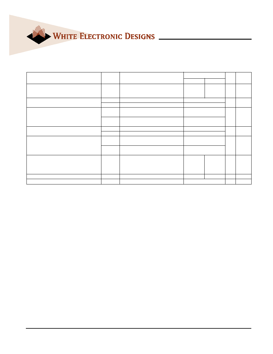
PIN NAMES
NC
NC
NC
NC
NC
NC
NC
NC
NC
NC
CS1\
CS0\
A0 A12
Address input (Multiplexed)
BA0-1
Select Bank
DQ0-63
Data Input/Output
CLK0
Clock input
CKE0, CKE1
Clock Enable input
CS0, CS1
Chip select Input
RAS
Row Address Strobe
CAS
Column Address Strobe
WE
Write Enable
DQM0-7
DQM
VDD
Power Supply (3.3V)
VSS
Ground
SDA
Serial data I/O
SCL
Serial clock
DNU
Do not use
NC
No Connect

2
White Electronic Designs Corporation (508) 485-4000 www.whiteedc.com
June 2003 Rev. 1
ECO #16373
WED3DG64128V-D1
White Electronic Designs Corp reserves the right to change products or specifications without notice.
FUNCTIONAL BLOCK DIAGRAM
5
5
5
5
5
5
5
7

3
White Electronic Designs Corporation (508) 485-4000 www.whiteedc.com
June 2003 Rev. 1
ECO #16373
WED3DG64128V-D1
White Electronic Designs Corp reserves the right to change products or specifications without notice.
(Voltage Referenced to: V
SS
= 0V, T
A
= 0∞C to +70∞C)
ABSOLUTE MAXIMUM RATINGS
Parameter
Symbol
Value
Units
Voltage on any pin relative to VSS
V
IN
, Vout
-1.0 ~ 4.6
V
Voltage on VDD supply relative to VSS
VDD, VDDQ
-1.0 ~ 4.6
V
Storage Temperature
TSTG
-55 ~ +150 ∞C
Power Dissipation
PD
16
W
Short Circuit Current
IOS
50
mA
Note: Permanent device damage may occur if "ABSOLUTE MAXIMUM RATINGS" are exceeded.
Functional operation should be restricted to recommended operating condition.
Exposure to higher than recommended voltage for extended periods of time could affect device reliability.
RECOMMENDED DC OPERATING CONDITIONS
Parameter
Symbol
Min
Typ
Max
Unit
Note
Supply Voltage
VDD
3.0
3.3
3.6
V
Input High Voltage
VIH
2.0
3.0 VDDQ+0.3 V
1
Input Low Voltage
VIL
-0.3
0.8
V
2
Output High Voltage
VOH
2.4
V
IOH= -2mA
Output Low Voltage
VOL
0.4
V
IOL= -2mA
Input Leakage Current
ILI
-10
10
µA
3
Note: 1. VIH (max)= 5.6V AC. The overshoot voltage duration is £ 3ns.
2. VIL (min)= -2.0V AC. The undershoot voltage duration is £ 3ns.
3. Any input 0V £ VIN £ VDDQ
Input leakage currents include Hi-Z output leakage for all bi-directional buffers with Tri-State
outputs.
CAPACITANCE
(T
A
= 23∞C, f = 1MHz, V
DD
= 3.3V, VREF=1.4V 6200mV)
Parameter
Symbol
Min
Max
Unit
Input Capacitance (A0-A12)
CIN1
-
15
pF
Input Capacitance (RAS,CAS,WE)
CIN2
-
15
pF
Input Capacitance (CKE0)
CIN3
-
15
pF
Input Capacitance (CLK0)
CIN4
-
20
pF
Input Capacitance (CS0)
CIN5
-
15
pF
Input Capacitance (DQM0-DQM7)
CIN6
-
15
pF
Input Capacitance (BA0-BA1)
CIN7
-
15
pF
Data input/output capacitance (DQ0-DQ63)
Cout
-
22
pF
Data input/output capacitance (CB0-7)
Cout 1
-
22
pF
4
White Electronic Designs Corporation (508) 485-4000 www.whiteedc.com
June 2003 Rev. 1
ECO #16373
WED3DG64128V-D1
White Electronic Designs Corp reserves the right to change products or specifications without notice.
OPERATING CURRENT CHARACTERISTICS
(V
CC
= 3.3V, T
A
= 0∞C to +70∞C)
Notes: 1. Measured with outputs open.
2. Refresh period is 64ms.
3. Unless otherwise noticed, input swing level is CMOS (VIH/VIL = VDDQ/VssQ)
Version
Parameter
Symbol
Conditions
133
100
Units Note
Operating Current
ICC1
Burst Length = 1
1,680
1,520
mA
1
(One bank active)
tRC ≥ tRC(min)
IOL = 0mA
Precharge Standby Current
ICC2P
CKE £ VIL(max), tCC = 10ns
130
mA
in Power Down Mode
ICC2PS
CKE & CLK £ VIL(max), tCC = •
120
Icc2N
CKE ≥ VIH(min), CS ≥ VIH(min), tcc = 10ns
Precharge Standby Current
Input signals are charged one time during 20
320
in Non-Power Down Mode
Icc2NS
CKE ≥ VIH(min), CLK £ VIL(max), tcc = •
mA
Input signals are stable
160
Active standby current in
ICC3P
CKE ≥ VIL(max), tCC = 10ns
160
mA
power-down mode
ICC3PS
CKE & CLK £ VIL(max), tcc = •
130
ICC3N
CKE ≥ VIH(min), CS ≥ VIH(min), tcc = 10ns
Active standby current in
Input signals are changed one time during 20ns 480
mA
non power-down mode
ICC3NS
CKE ≥ VIH(min), CLK £ VIL(max), tcc = •
input signals are stable
360
mA
Io = mA
Operating current (Burst mode)
ICC4
Page burst
1,680
1,440
mA
1
4 Banks activated
tCCD = 2CLK
Refresh current
ICC5
tRC ≥ tRC(min)
2,720
2,560
mA
2
Self refresh current
ICC6
CKE £ 0.2V
115
mA
5
White Electronic Designs Corporation (508) 485-4000 www.whiteedc.com
June 2003 Rev. 1
ECO #16373
WED3DG64128V-D1
White Electronic Designs Corp reserves the right to change products or specifications without notice.
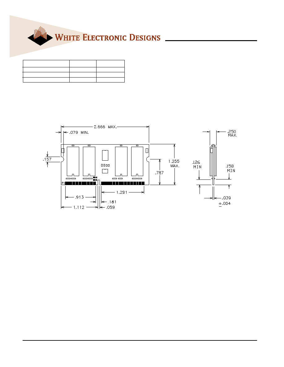
ALL DIMENSIONS ARE IN INCHES
PACKAGE DIMENSIONS
Part number
Speed
Cas Latency
WED3DG64128V10D1
100MHz
CL=2
WED3DG64128V7D1
133MHz
CL=2
WED3DG64128V75D1
133MHz
CL=3
Note: For industrial temperature range product, add an "I" to the end of the part
number.