
1
White Electronic Designs Corporation ∑ (602) 437-1520 ∑ www.wedc.com
White Electronic Designs
WED3DL3216V
January, 2004
Rev. 0
White Electronic Designs Corp. reserves the right to change products or specifi cations without notice.
16Mx32 SDRAM
40% Space Savings vs. Monolithic Solution
Reduced System Inductance and Capacitance
3.3V Operating Supply Voltage
Fully Synchronous to Positive Clock Edge
Clock Frequencies of 100MHz - 133MHz
Burst Operation
∑ Sequential or Interleave
∑ Burst Length = Programmable 1, 2, 4, 8
or
Full
Page
∑ Burst Read and Write
∑ Multiple Burst Read and Single Write
Data Mask Control Per Byte
Auto and Self Refresh
Automatic and Controlled Precharge Commands
Suspend Mode and Power Down Mode
119 Pin BGA, 17mm x 23mm
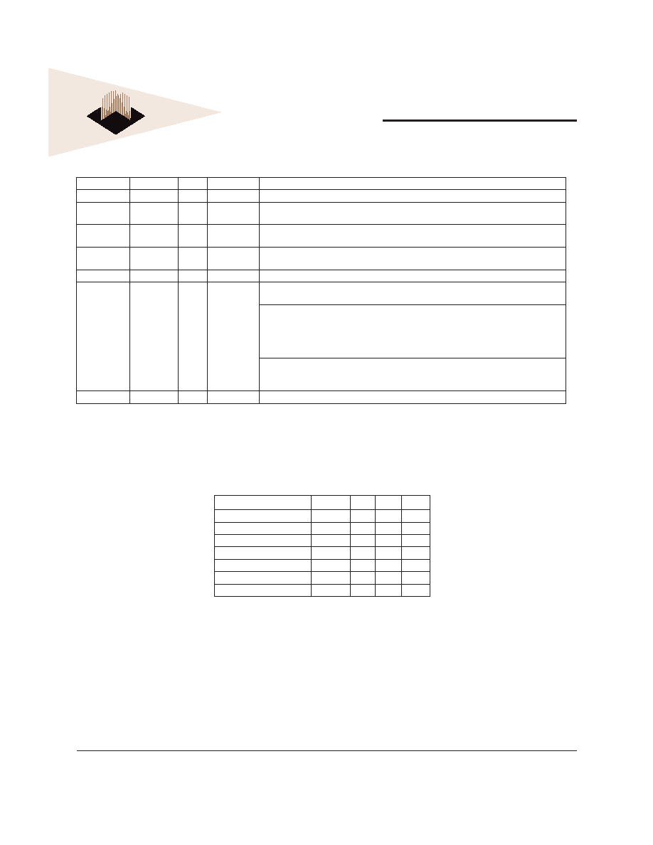
PIN DESCRIPTION
PIN CONFIGURATION
(Top view)
The WED3DL3216V is an 16Mx32 Synchronous DRAM
confi gured as 4x4Mx32. The SDRAM BGA is constructed
with two 16Mx16 SDRAM die mounted on a multi-layer
laminate substrate and packaged in a 119 lead, 17mm
by 23mm, BGA.
The WED3DL3216V is available in clock speeds
of 133MHz, 125MHz, and 100MHz. The range of
operating frequencies, programmable burst lengths and
programmable latencies allow the same device to be
useful for a variety of high bandwidth, high performance
memory system applications.
The package and design provides performance
enhancements via a 50% reduction in capacitance vs.
two monolithic devices. The design includes internal
ground and power planes which reduces inductance
on the ground and power pins allowing for improved
decoupling and a reduction in system noise.
1
2
3
4
5
6
7
A
V
CCQ
NC
BA0
NC
A10
A7
V
CCQ
A
B
NC
NC
A12
CAS#
A11
NC
NC
B
C
NC
NC
BA1
V
CC
A9
A8
NC
C
D
DQC
NC
V
SS
NC
V
SS
NC
DQB
D
E
DQC
DQC
V
SS
CE#
V
SS
DQB
DQB
E
F
V
CCQ
DQC
V
SS
RAS#
V
SS
DQB
V
CCQ
F
G
DQC
DQC
DQMC
NC
DQMB
DQB
DQB
G
H
DQC
DQC
V
SS
CKE
V
SS
DQB
DQB
H
J
V
CCQ
V
CC
NC
V
CC
NC
V
CC
V
CCQ
J
K
DQD
DQD
V
SS
CK
V
SS
DQA
DQA
K
L
DQD
DQD
DQMD
NC
DQMA
DQA
DQA
L
M
V
CCQ
DQD
V
SS
WE#
V
SS
DQA
V
CCQ
M
N
DQD
DQD
V
SS
A1
V
SS
DQA
DQA
N
P
DQD
NC
V
SS
A0
V
SS
NC
DQA
P
R
NC
A6
NC
V
CC
NC
A2
NC
R
T
NC
NC
A5
A4
A3
NC
NC
T
U
V
CCQ
NC
NC
NC
NC
NC
V
CCQ
U
1
2
3
4
5
6
7
A0 ≠ A12
Address Bus
BA0-1
Bank Select Addresses
DQ Data
Bus
CK
Clock
CKE
Clock Enable
DQM Data
Input/Output
Mask
RAS#
Row Address Strobe
CAS#
Column Address Strobe
CE#
Chip Enable
V
CC
Power Supply pins, 3.3V
V
CCQ
Data Bus Power Supply pins,3.3V
V
SS
Ground pins
FEATURES
DESCRIPTION

2
White Electronic Designs Corporation ∑ (602) 437-1520 ∑ www.wedc.com
White Electronic Designs
WED3DL3216V
January, 2004
Rev. 0
White Electronic Designs Corp. reserves the right to change products or specifi cations without notice.
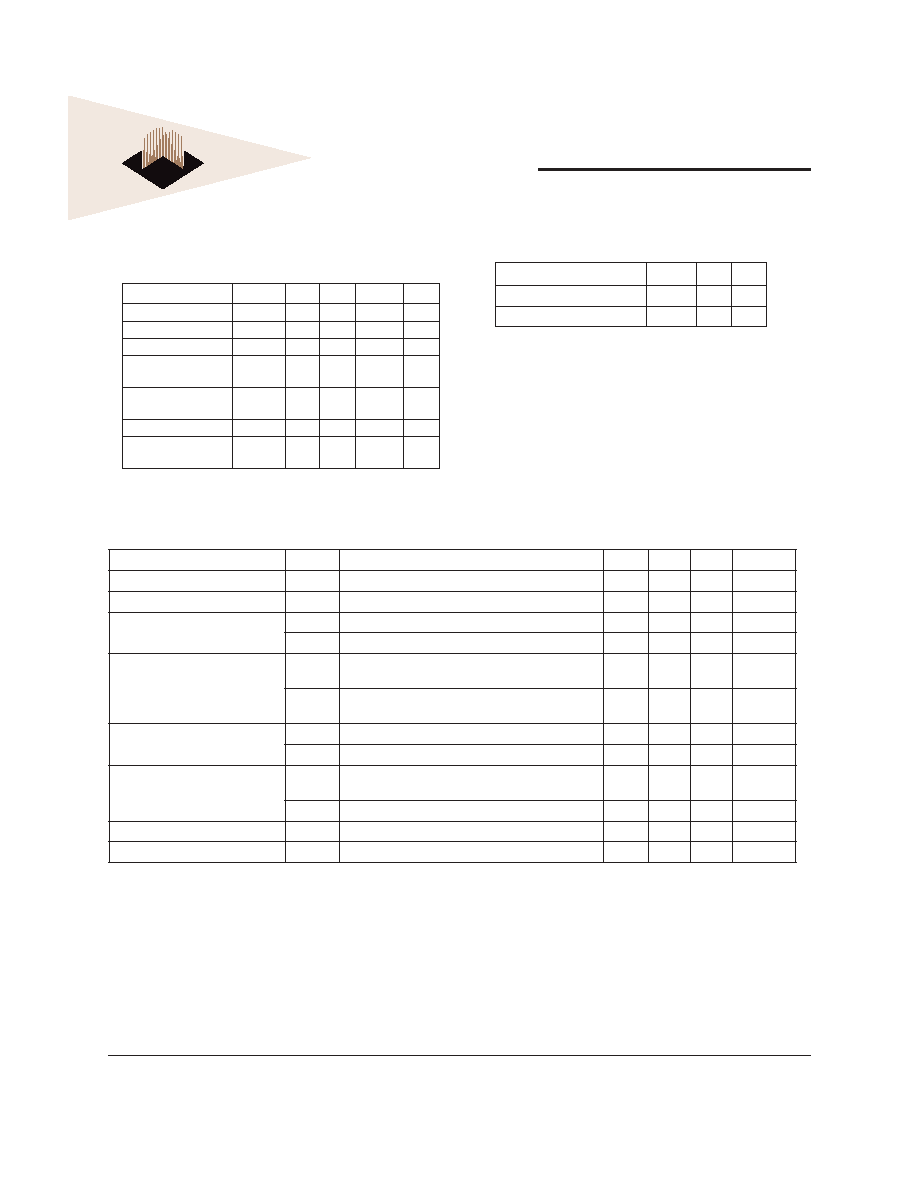
16MX32 SDRAM BLOCK DIAGRAM
ADDR0-12
BA0
BA1
DQMA
DQMB
CE#
RAS#
CAS#
WE#
CK
CKE
DQMD
DQMC
CS#
RAS#
CAS#
WE#
CK
CKE
LDQM#
UDQM#
BA1
BA0
A0
A12
A10
A9
A8
A7
A6
A5
A4
A3
A2
A1
A11
CS#
RAS#
CAS#
WE#
CK
CKE
LDQM#
UDQM#
BA1
BA0
A0
A12
A10
A9
A8
A7
A6
A5
A4
A3
A2
A1
A11
DQ0-7
DQ8-15
DQ0-7
DQ8-15
DQA
DQD
DQC
DQB
DQ0-31
3
White Electronic Designs Corporation ∑ (602) 437-1520 ∑ www.wedc.com
White Electronic Designs
WED3DL3216V
January, 2004
Rev. 0
White Electronic Designs Corp. reserves the right to change products or specifi cations without notice.
Parameter
Symbol
Min
Max
Units
Power Supply Voltage
V
CC
/V
CCQ
-1.0
+4.6
V
Input Voltage
V
IN
-1.0
+4.6
V
Output Voltage
V
OUT
-1.0
+4.6
V
Operating Temperature
T
OPR
-0
+70
∞C
Storage Temperature
T
TSG
-55
+125
∞C
Power Dissipation
P
D
--
1.5
W
Short Circuit Output Current
I
OS
--
50
mA
I
NPUT
/O
UTPUT
F
UNCTIONAL
D
ESCRIPTION
ABSOLUTE MAXIMUM RATINGS*
* Stress greater than those listed under "Absolute Maximum Ratings" may cause permanent damage to the device. This is a stress rating only and functional operation of the device
at these or any other conditions greater than those indicated in the operational sections of this specifi cation is not implied. Exposure to absolute maximum rating conditions for
extended periods may affect reliability.
Symbol
Type
Signal
Polarity
Function
CK
Input
Pulse
Positive Edge The system clock input. All of the SDRAM inputs are sampled on the rising edge of the clock
CKE
Input
Level
Active High
Activates the CK signal when high and deactivates the CK signal when low. By deactivating the
clock, CKE low initiates the Power Down mode, Suspend mode, or the Self Refresh mode
CE#
Input
Pulse
Active Low
CE# disable or enable device operation by masking or enabling all inputs except CK, CKE and
DQM.
RAS#, CAS#,
WE#
Input
Pulse
Active Low
When sampled at the positive rising edge of the clock, CAS#, RAS# and WE# defi ne the
operation to be executed by the SDRAM
BA0, BA1
Input
Level
-
Selects which SDRAM bank is to be active.
A0-12
Input
Level
-
During a Bank Activate command cycle, A0-12 defi nes the row address (RA0-12) when sampled
at the rising clock edge.
During a Read or Write command cycle, A0-9 defi nes the column address (CA0-9) when
sampled at the rising edge of the clock. In addition to the row address, A10/AP is used to
invoke Autoprecharge operation at the end of the Burst Read or Write cycle. If A10/AP is high,
autoprecharge is selected and BA0, BA1 defi nes the bank to be precharged. If A10/AP is low,
autoprecharge is disabled.
During a Precharge command cycle, A10/AP is used in conjunction with BA0, BA1 to control
which bank(s) to precharge. If A10/AP is high, all banks will be precharged regardless of the
state of BA0, BA1. If A10/AP is low, than BA0, BA1 is used to defi ne which bank to precharge.
DQ
Input/Output
Level
-
Data Input/Output are multiplexed on the same pins
4
White Electronic Designs Corporation ∑ (602) 437-1520 ∑ www.wedc.com
White Electronic Designs
WED3DL3216V
January, 2004
Rev. 0
White Electronic Designs Corp. reserves the right to change products or specifi cations without notice.
Parameter
Symbol
Conditions
-7
-8
-10
Units
Operating Current (One Bank Active)
1
I
CC1
Burst Length = 1, t
RC
t
RC
(min), I
OL
= 0mA
300
280
260
mA
Operating Current (Burst Mode)
1
I
CC4
Page Burst, 4 banks active, t
CCD
= 2 clocks
300
280
260
mA
Precharge Standby Current
in Power Down Mode
I
CC2P
CKE V
IL
(max), t
CC
= 15ns
2
2
2
mA
I
CC2PS
CKE, CK V
IL
(max), t
CC
= , Inputs Stable
2
2
2
mA
Precharge Standby Current
in Non-Power Down Mode
I
CC1N
CKE = V
IH
, t
CC
= 15ns
Input Change one time every 30ns
140
140
140
mA
I
CC1NS
CKE V
IH
(min), t
CC
=
No Input Change
70
70
70
mA
Precharge Standby Current
in Power Down Mode
I
CC3P
CKE V
IL
(max), t
CC
= 15ns
12
12
12
mA
I
CC3PS
CKE V
IL
(max), t
CC
=
12
12
12
mA
Active Standby Current in
Non-Power Down Mode
(One Bank Active)
I
CC3N
CKE = V
IH
, t
CC
= 15ns
Input Change one time every 30ns
60
60
60
mA
I
CC3NS
CKE V
IH
(min), t
CC
= , No Input Change
50
50
50
mA
Refresh Current
2
I
CC5
t
RC
t
RC
(min)
600
570
550
mA
Self Refresh Current
I
CC6
CKE 0.2V
6.5
6.5
6.5
mA
OPERATING CURRENT CHARACTERISTICS
(V
CC
= 3.3V, T
A
= 0∞C
TO
70∞C; C
OMMERCIAL
OR
TA = -40∞C
TO
+85∞C; I
NDUSTRIAL
)
NOTES:
1. Measured with outputs open.
2. Refresh period is 64ms.
RECOMMENDED DC OPERATING CONDITIONS
(V
OLTAGE
R
EFERENCED
TO
: V
SS
= 0V, 0∞C T
A
70∞C; C
OMMERCIAL
OR
T
A
= -40∞C
TO
+85∞C; I
NDUSTRIAL
)
CAPACITANCE
(T
A
= 25∞C, f = 1MH
Z
, V
CC
= 3.3V)
Parameter
Symbol
Max
Unit
Input Capacitance
C
I1
4
pF
Input/Output Capacitance (DQ)
C
OUT
5
pF
Parameter
Symbol
Min
Typ
Max
Unit
Supply Voltage
V
CC
/V
CCQ
3.0
3.3 3.6
V
Input High Voltage
V
IH
2.0
3.0
V
CC
+0.3
V
Input Low Voltage
V
IL
-0.3
--
0.8
V
Output High Voltage
(I
OH
= -2mA)
V
OH
2.4
--
--
V
Output Low Voltage
(I
OL
= 2mA)
V
OL
--
--
0.4
V
Input Leakage Voltage
I
IL
-5
--
5
µA
Output Leakage
Voltage
I
OL
-5
--
5
µA

5
White Electronic Designs Corporation ∑ (602) 437-1520 ∑ www.wedc.com
White Electronic Designs
WED3DL3216V
January, 2004
Rev. 0
White Electronic Designs Corp. reserves the right to change products or specifi cations without notice.
Parameter
Symbol
133MH
Z
125MH
Z
100MH
Z
Units
Min
Max
Min
Max
Min
Max
CL = 3
t
CC
7
1000
8
1000
10
1000
ns
CL = 2
t
CC
7.5
1000
10
1000
12
1000
Clock to valid Output delay
1,2
t
SAC
5.4
6
7
ns
Output Data Hold Time
2
t
OH
3
3
3
ns
Clock HIGH Pulse Width
3
t
CH
2.5
3
3
ns
Clock LOW Pulse Width
3
t
CL
2.5
3
3
ns
Input Setup Time
3
t
SS
1.5
2
2
ns
Input Hold Time
3
t
SH
0.8
1
1
ns
CK to Output Low-Z
2
t
SLZ
2
2
2
ns
CK to Output High-Z
t
SHZ
5.4
6
7
ns
Row Active to Row Active Delay
4
t
RRD
24
20
20
ns
RAS to CAS Delay
4
t
RCD
24
20
20
ns
Row Precharge Time
4
t
RP
24
20
20
ns
Row Active Time
4
t
RAS
60
10,000
50
10,000
50
10,000
ns
Row Cycle Time - Operation
4
t
RC
90
70
80
ns
Row Cycle Time - Auto Refresh
4,8
t
RFC
90
70
80
ns
Last Data in to New Column Address Delay
5
t
CDL
1
1
1
CK
Last Data in to Row Precharge
5
t
RDL
1
1
1
CK
Last Data in to Burst Stop
5
t
BDL
1
1
1
CK
Column Address to Column Address Delay
6
t
CCD
1.5
1.5
1.5
CK
Number of Valid OutputData
7
2
2
2
ea
1
1
2
SDRAM AC CHARACTERISTICS
NOTES:
1.
Parameters depend on programmed CAS latency.
2.
If clock rise time is longer than 1ns (t
RISE
/2 -0.5)ns should be added to the parameter.
3.
Assumed input rise and fall time = 1ns. If t
RISE
or t
FALL
are longer than 1ns. [(t
RISE
= t
FALL
)/2] - 1ns should be added to the parameter.
4.
The minimum number of clock cycles required is detemined by dividing the minimum time required by the clock cycle time and then rounding up to the next higher integer.
5.
Minimum delay is required to complete write.
6.
All devices allow every cycle column address changes.
7.
In case of row precharge interrupt, auto precharge and read burst stop.