
1
White Electronic Designs Corporation ∑ (602) 437-1520 ∑ www.wedc.com
WED3EG6418S-D4
Oct. 2002
Rev. # 0
FINAL
White Electronic Designs Corp. reserves the right to change products or specifi cations without notice.
128MB- 16Mx64 DDR SDRAM UNBUFFERED W/PLL
DESCRIPTION
The WED3DG6418S is a 16Mx64 Double Data Rate
SDRAM memory module based on 128Mb DDR
SDRAM component. The module consists of eight
16Mx8 DDR SDRAMs in 66 pin TSOP package
mounted on a 200 Pin FR4 substrate.
Synchronous design allows precise cycle control
with the use of system clock. Data I/O transactions
are possible on both edges and Burst Lenths allow
the same device to be useful for a variety of high
bandwidth, high performance memory system
applications.
FEATURES
Double-data-rate architecture
Speed of 100MHz, 133MHz and 166MHz
Bi-directional data strobes (DQS)
Differential clock inputs (CK & CK#)
Programmable Read Latency 2,2,5 (clock)
Programmable Burst Length (2,4,8)
Programmable Burst type (sequential & interleave)
Edge aligned data output, center aligned data input
Auto and self refresh
Serial presence detect
JEDEC standard 200 pin SO-DIMM package
Power Supply: 2.5V ± 0.25V
2
White Electronic Designs Corporation ∑ (602) 437-1520 ∑ www.wedc.com
WED3EG6418S-D4
Oct. 2002
Rev. # 0
FINAL
White Electronic Designs Corp. reserves the right to change products or specifi cations without notice.
PIN CONFIGURATIONS
PIN NAMES
A0 ≠ A11
Address input (Multiplexed)
BA0-BA1
Bank Select Address
DQ0-DQ63
Data Input/Output
DQS0-DQS8
Data Strobe Input/Output
CK0
Clock input
CK0#
Clock input
CKE0
Clock Enable Input
CS0#
Chip select Input
RAS#
Row Address Strobe
CAS#
Column Address Strobe
WE#
Write Enable
DQM0-DQM8
Data-In Mask
V
CC
Power Supply (2.5V)
V
CCQ
Power Supply for DQS (2.5V)
V
SS
Ground
V
REF
Power Supply for Reference
V
CCSPD
Serial EEPROM Power Supply
(2.3V to 3.6V)
SDA
Serial data I/O
SCL
Serial clock
SA0-SA2
Address in EEPROM
V
CCID
V
CC
Identifi cation Flag
NC
No Connect
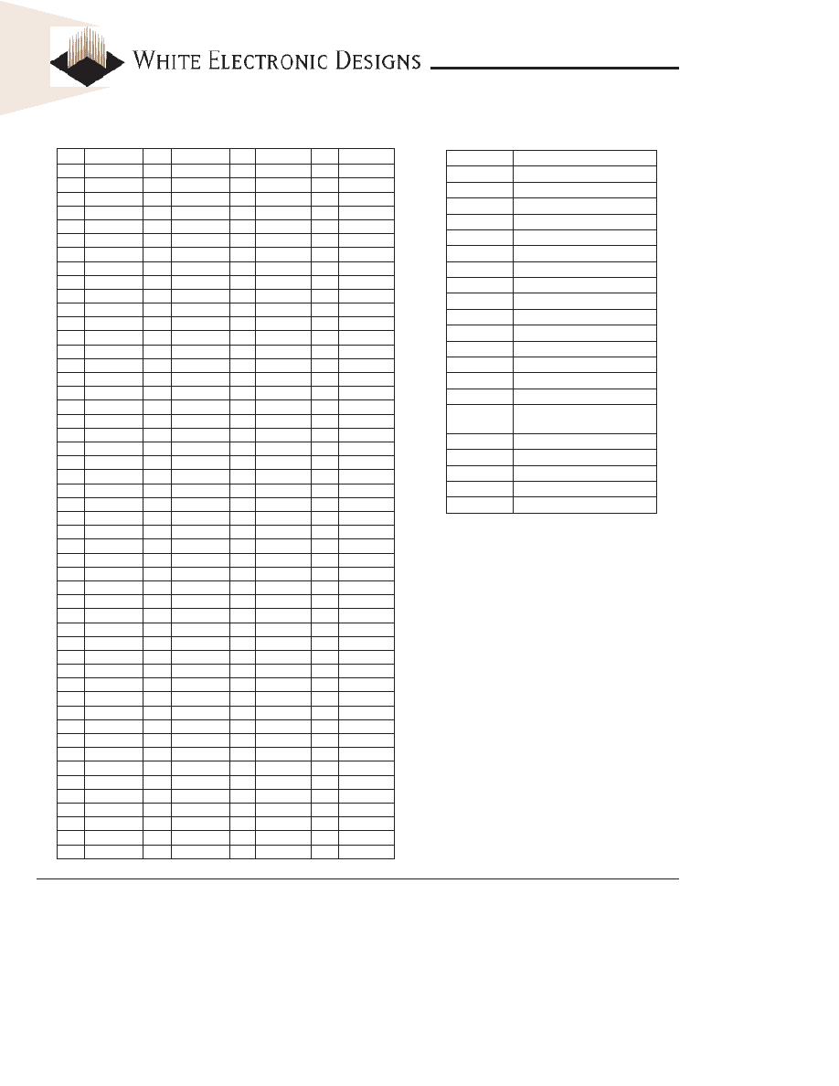
Pin
Symbol
Pin
Symbol
Pin
Symbol
Pin
Symbol
1
V
REF
51
V
SS
101
A9
151
DQ42
2
V
REF
52
V
SS
102
A8
152
DQ46
3
V
SS
53
DQ19
103
V
SS
153
DQ43
4
V
SS
54
DQ23
104
V
SS
154
DQ47
5
DQ0
55
DQ24
105
A7
155
V
CC
6
DQ4
56
DQ28
106
A6
156
V
CC
7
DQ1
57
V
CC
107
A5
157
V
CC
8
DQ5
58
V
CC
108
A4
158
NC
9
V
CC
59
DQ25
109
A3
159
V
SS
10
V
CC
60
DQ29
110
A2
160
NC
11
DQS0
61
DQS3
111
A1
161
V
SS
12
DM0
62
DM3
112
A0
162
V
SS
13
DQ2
63
V
SS
113
V
CC
163
DQ48
14
DQ6
64
V
SS
114
V
CC
164
DQ52
15
V
SS
65
DQ26
115
A10/AP
165
DQ49
16
V
SS
66
DQ30
116
BA1
166
DQ53
17
DQ3
67
DQ27
117
BA0
167
V
CC
18
DQ7
68
DQ31
118
RAS#
168
V
CC
19
DQ8
69
V
CC
119
WE#
169
DQS6
20
DQ12
70
V
CC
120
CAS#
170
DM6
21
V
CC
71
NC
121
CSO
171
DQ50
22
V
CC
72
NC
122
NC
172
DQ54
23
DQ9
73
NC
123
NC
173
V
SS
24
DQ13
74
NC
124
NC
174
V
SS
25
DQS1
75
V
SS
125
V
SS
175
DQ51
26
DM1
76
V
SS
126
V
SS
176
DQ55
27
V
SS
77
DQS8
127
DQ32
177
DQ56
28
V
SS
78
DM8
128
DQ36
178
DQ60
29
DQ10
79
NC
129
DQ33
179
V
CC
30
DQ14
80
NC
130
DQ37
180
V
CC
31
DQ11
81
V
CC
131
V
CC
181
DQ57
32
DQ15
82
V
CC
132
V
CC
182
DQ61
33
V
CC
83
NC
133
DQS4
183
DQS7
34
V
CC
84
NC
134
DM4
184
DM7
35
CK0
85
NC
135
DQ34
185
V
SS
36
V
CC
86
NC
136
DQ38
186
V
SS
37
CK0#
87
V
SS
137
V
SS
187
DQ58
38
V
SS
88
V
SS
138
V
SS
188
DQ62
39
V
SS
89
NC
139
DQ35
189
DQ59
40
V
SS
90
V
SS
140
DQ39
190
DQ63
41
DQ16
91
NC
141
DQ40
191
V
CC
42
DQ20
92
V
CC
142
DQ44
192
V
CC
43
DQ17
93
V
CC
143
V
CC
193
SDA
44
DQ21
94
V
CC
144
V
CC
194
SA0
45
V
CC
95
NC
145
DQ41
195
SCL
46
V
CC
96
CKE0
146
DQ45
196
SA1
47
DQS2
97
NC
147
DQS5
197
V
CCSPD
48
DM2
98
NC
148
DM5
198
SA2
49
DQ18
99
NC
149
V
SS
199
V
CCID
50
DQ22
100
A11
150
V
SS
200
NC
3
White Electronic Designs Corporation ∑ (602) 437-1520 ∑ www.wedc.com
WED3EG6418S-D4
Oct. 2002
Rev. # 0
FINAL
White Electronic Designs Corp. reserves the right to change products or specifi cations without notice.
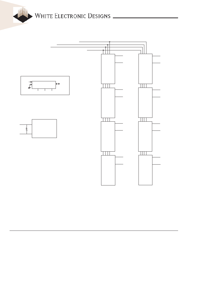
FUNCTIONAL BLOCK DIAGRAM
WE#,RAS#CAS#
SO#
CKE0
BA0,BA1,A0-A11
DQ0-7
DQ0-7
DQM0
DM
U1
DQ0-7
DQ32-39
DQM4
DM
U3
DQ0-7
DQ8-15
DQM1
DM
U2
DQ0-7
DQ40-479
DQM5
DM
U4
DQ0-7
DQ16-23
DQM2
DM
U5
DQ0-7
DQ48-55
DQM6
DM
U7
DQ0-7
DQ24-31
DQM3
DM
U6
DQ0-7
DQ56-63
DQM7
DM
U8
SERIAL PD
SCL
SDA
SA0
SA1 SA2
WP
A0
A1
A2
CK0
120
CK0#
DDR SDRAM U1
DDR SDRAM U2
DDR SDRAM U3
DDR SDRAM U4
DDR SDRAM U4
DDR SDRAM U6
DDR SDRAM U7
DDR SDRAM U8
PLL
4
White Electronic Designs Corporation ∑ (602) 437-1520 ∑ www.wedc.com
WED3EG6418S-D4
Oct. 2002
Rev. # 0
FINAL
White Electronic Designs Corp. reserves the right to change products or specifi cations without notice.
Absolute Maximum Ratings
Parameter
Symbol
Value
Units
Voltage on any pin relative to V
SS
V
IN
, V
OUT
-0.5 ~ 3.6
V
Voltage on V
CC
supply relative to V
SS
V
CC
, V
CCQ
-1.0 ~ 3.6
V
Storage Temperature
T
STG
-55 ~ +150
∞C
Power Dissipation
P
D
8
W
Short Circuit Current
I
OS
50
mA
Note:
Permanent device damage may occur if "ABSOLUTE MAXIMUM RATINGS" are exceeded.
Functional operation should be restricted to recommended operating condition.
Exposure to higher than recommended voltage for extended periods of time could affect device reliability.
DC CHARACTERISTICS
(t
A
= 0 to 70∞C, V
CC
= 2.5V ± 0.2V)
Parameter
Symbol
Min
Max
Unit
Supply Voltage
V
CC
2.3
2.7
V
Supply Voltage
V
CCQ
2.3
2.7
V
Reference Voltage
V
REF
V
CCQ
/2-50mV
V
CCQ
/2+50mV
V
Termination Voltage
V
TT
V
REF
-0.04
V
REF
+0.04
V
Input High Voltage
V
IH
V
REF
+0.15
V
CCQ
+0.3
V
Input Low Voltage
V
IL
-0.3
V
REF
+0.15
V
Output High Voltage
V
OH
V
TT
+0.76
--
V
Output Low Voltage
V
OL
--
V
TT
-0.76
V
CAPACITANCE
(t
A
= 23∞C, f = 1MHz, V
CC
= 3.3V, V
REF
=1.4V ± 200mV)
Parameter
Symbol
Min
Max
Unit
Input Capacitance (A0-A12)
C
IN
1
-
34
pF
Input Capacitance (RAS#,CAS#,WE#)
C
IN
2
-
34
pF
Input Capacitance (CKE0)
C
IN
3
-
34
pF
Input Capacitance (CK0, CK0#)
C
IN
4
-
30
pF
Input Capacitance (CS0#)
C
IN
5
-
30
pF
Input Capacitance (DQM0-DQM8)
C
IN
6
-
10
pF
Input Capacitance (BA0-BA1)
C
IN
7
-
45
pF
Data input/output capacitance (DQ0-DQ63)(DQS)
C
OUT
-
10
pF
5
White Electronic Designs Corporation ∑ (602) 437-1520 ∑ www.wedc.com
WED3EG6418S-D4
Oct. 2002
Rev. # 0
FINAL
White Electronic Designs Corp. reserves the right to change products or specifi cations without notice.
I
DD
SPECIFICATIONS AND TEST CONDITIONS
(Recommended operating conditions, t
A
= 0 to 70∞C, V
CCQ
= 2.5V ± 0.2V, V
CC
= 2.5V ± 0.2V)
* Module I
DD
was calculated on the basis of component I
DD
and can be different measured according to DQ loading cap.
Parameter
Symbol
Conditions
DDR333@CL=2.5
Max
DDR266@CL=2, 2.5
Max
DDR200@CL=2
Max
Units
Operating Current
I
DD0
One device bank; Active = Precharge;
t
RC
=t
RC
(MIN); t
CK
=t
CK
(MIN); DQ, DM and DQS inputs changing
once per clock cycle; Address and control
inputs changing once every two cycles.
840
760
680
mA
Operating Current
I
DD1
One device banks; Active-Read-Precharge;
Burst = 2; t
RC
=t
RC
(MIN); t
CK
=t
CK
(MIN); l
OUT
=0mA; Address and control inputs
changing once per clock cycle.
1040
960
880
mA
Precharge Power-
Down Standby Current
I
DD2P
All device bank idle; Power-down mode;
t
CK
=t
CK
(MIN); CKE=(low)
24
24
24
mA
Idle Standby Current
I
DD2F
CS# = High; All device banks idle;
t
CK
=t
CK
(MIN); CKE = high; Address and other
control inputs changing once per clock cycle.
V
IN
= V
REF
for DQ, DQS and DM.
200
180
160
mA
Active Power-Down
Standby Current
I
DD3P
One device bank active; Power-down mode;
t
CK
(MIN); CKE=(low)
280
280
225
mA
Active Standby Current
I
DD3N
CS# = High; CKE = High; One device
bank; Active-Precharge; t
RC
=t
RAS
(MAX);
t
CK
=t
CK
(MIN); DQ, DM and DQS inputs
changing twice per clock cycle; Address and
other control inputs changing once per clock
cycle
495
440
360
mA
Operating Current
I
DD4R
Burst = 2; Reads; Continous burst; Once
device bank active; Address and control
inputs changing once per clock cycle;
t
CK
=t
CK
(MIN); I
OUT
=0mA
1280
1140
960
mA
Operating Current
I
DD4W
Burst=2; Writes; Continous burst; Once
device bank active; Address and control
inputs changing once per clock cycle;
t
CK
=t
CK
(MIN); DQ,DM and DQS inputs
changing twice per clock cycle.
1216
1040
815
mA
Auto Refresh Current
I
DD5
t
RC
=t
RC
(MIN)
1520
1440
1315
mA
Self Refresh Current
I
DD6
CKE £ 0.2V
16
16
16
mA
Operating Current
I
DD7A
Four bank interleaving Reads (BL=4)
with auto precharge with t
RC
=t
RC
(MIN);
t
CK
=t
CK
(MIN); Address and control input
change only during Active Read or Write
commands.
2640
2400
1920
mA

6
White Electronic Designs Corporation ∑ (602) 437-1520 ∑ www.wedc.com
WED3EG6418S-D4
Oct. 2002
Rev. # 0
FINAL
White Electronic Designs Corp. reserves the right to change products or specifi cations without notice.
I
DD1
: OPERATING CURRENT: ONE
BANK
1. Typical Case : V
CC
= 2.5V, T = 25∞C
2. Worst Case : V
CC
= 2.7V, T = 10∞C
3. Only one bank is accessed with t
RC
(min), Burst Mode,
Address and Control inputs on NOP edge are changing
once per clock cycle.
I
OUT
= 0mA
4. Timing patterns
-DDR200 (100Mhz, CL = 2) : t
CK
= 10ns, CL2, BL = 4,
t
RCD
= 2*t
CK
, t
RAS
= 5*t
CK
Read : A0 N R0 N N P0 N A0 N - repeat the same
timing with random address changing; 50% of data
changing at every burst
-DDR266B (133Mhz, CL = 2.5): t
CK
= 7.5ns, CL = 2.5,
BL = 4, t
RCD
= 3*t
CK
, t
RC
= 9*t
CK
, t
RAS
= 5*t
CK
Read : A0 N N R0 N P0 N N N A0 N - repeat the
same timing with random address changing; 50% of
data changing at every burst
-DDR266A (133Mhz, CL = 2) : t
CK
= 7.5ns, CL = 2, BL
= 4, t
RCD
= 3*t
CK
, t
RC
= 9*t
CK
, t
RAS
= 5*t
CK
Read : A0 N N R0 N P0 N N N A0 N - repeat the
same timing with random address changing; 50% of
data changing at every burst
-DDR333 (166MHz, CL = 2.5) : t
CK
= 6ns, CL = 2.5, BL
= 4, t
RCD
= 10*t
CK
, t
RAS
= 7*t
CK
Read " A0 N N R0 N P0 N N N A0 N - repeat the same
timing with random address changing; 50% of data
changing at every burst.
I
DD7A
: OPERATING CURRENT : FOUR
BANK OPERATION
1. Typical Case : V
cc
= 2.5V, T = 25∞C
2. Worst Case : V
cc
= 2.7V, T = 10∞C
3. Four banks are being interleaved with t
RC
(min), Burst
Mode, Address and Control inputs on NOP edge are not
changing.
I
OUT
= 0mA
4. Timing patterns
- DDR200 (100Mhz, CL = 2) : t
CK
= 10ns, CL2, BL =
4, t
RRD
= 2*t
CK
, t
RCD
= 3*t
CK
, Read with autoprecharge
Read : A0 N A1 R0 A2 R1 A3 R2 A0 R3 A1 R0 -
repeat the same timing with random address
changing; 100% of data changing at every burst
-DDR266B (133Mhz, CL = 2.5) : t
CK
= 7.5ns, CL =
2.5, BL = 4, t
RRD
= 2*t
CK
, t
RCD
= 3*t
CK
Read with autoprecharge
Read : A0 N A1 R0 A2 R1 A3 R2 N R3 A0 N A1
R0 - repeat the same timing with random address
changing; 100% of data changing at every burst
-DDR266A (133Mhz, CL = 2) : t
CK
= 7.5ns, CL2 = 2,
BL = 4, t
RRD
= 2*t
CK
, t
RCD
= 3*t
CK
Read : A0 N A1 R0 A2 R1 A3 R2 N R3 A0 N A1
R0 - repeat the same timing with random address
changing; 100% of data changing at every burst
-DDR333 (166MHz, CL = 2.5) : t
CK
= 6ns, CL =
2.5, BL = 4, t
RRD
= 2*t
CK
, t
RCD
= 3*t
CK
, Read with
autoprecharge
Read : A0 N A1 R0 A2 R1 A3 R2 N R3 A0 N A1
R0 - repeat the same timing with random address
changing; 100% of data changing at every burst
Legend : A = Activate, R = Read, W = Write, P = Precharge, N = NOP
DETAILED TEST CONDITIONS FOR DDR SDRAM I
DD1
& I
DD7A
7
White Electronic Designs Corporation ∑ (602) 437-1520 ∑ www.wedc.com
WED3EG6418S-D4
Oct. 2002
Rev. # 0
FINAL
White Electronic Designs Corp. reserves the right to change products or specifi cations without notice.
ORDER INFORMATION
Part Number
Speed
CAS Latency
WED3EG6418S335D4
166MHz/333Mbps CL=2.5
WED3EG6418S262D4
133MHz/266Mbps
CL=2
WED3EG6418S265D4
133MHz/266Mbps
CL=2.5
WED3EG6418S202D4
100MHz/200Mbps
CL=2
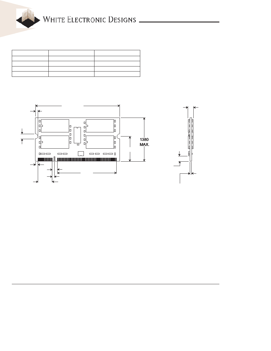
PACKAGE DIMENSIONS
ALL DIMENSIONS ARE IN INCHES
2.666 MAX.
.079
.157+/-.004
.091 REF.
.449
.165
.071
1.866
.787
.150 MAX
.157
MIN.
.039±.004
PI