WED416S8030A-SI
1
White Electronic Designs Corporation ∑ (602) 437-1520 ∑ www.wedc.com
White Electronic Designs
October 2004
Rev. 4
White Electronic Designs Corp. reserves the right to change products or specifi cations without notice.
2Mx16x 4 Banks Synchronous DRAM
FEATURES
Single 3.3V power supply
Fully Synchronous to positive Clock Edge
SDRAM CAS Latentency = 3 (100MHz), 2 (83MHz)
Burst
Operation
∑ Sequential or Interleave
∑ Burst length = programmable 1,2,4,8 or full page
∑ Burst Read and Write
∑ Multiple Burst Read and Single Write
DATA Mask Control per byte
Auto Refresh (CBR) and Self Refresh
∑ 4096 refresh cycles across 64ms
Automatic and Controlled Precharge Commands
Suspend Mode and Power Down Mode
DESCRIPTION
The WED416S8030AxxSI is 134,217,728 bits of
synchronous high data rate DRAM organized as 4 x
2,097, 152 words x 16 bits. Synchronous design allows
precise cycle control with the use of system clock, I/O
transactions are possible on every clock cycle. Range of
operating frequencies, programmable burst lengths and
programmable latencies allow the same device to be useful
for a variety of high bandwidth, high performance memory
system applications.
Available in a 54 pin TSOP type II package the
WED416S4030AxxSI is tested over the industrial temp
range (-40∞C to +85∞C) providing a solution for rugged
main memory applications.
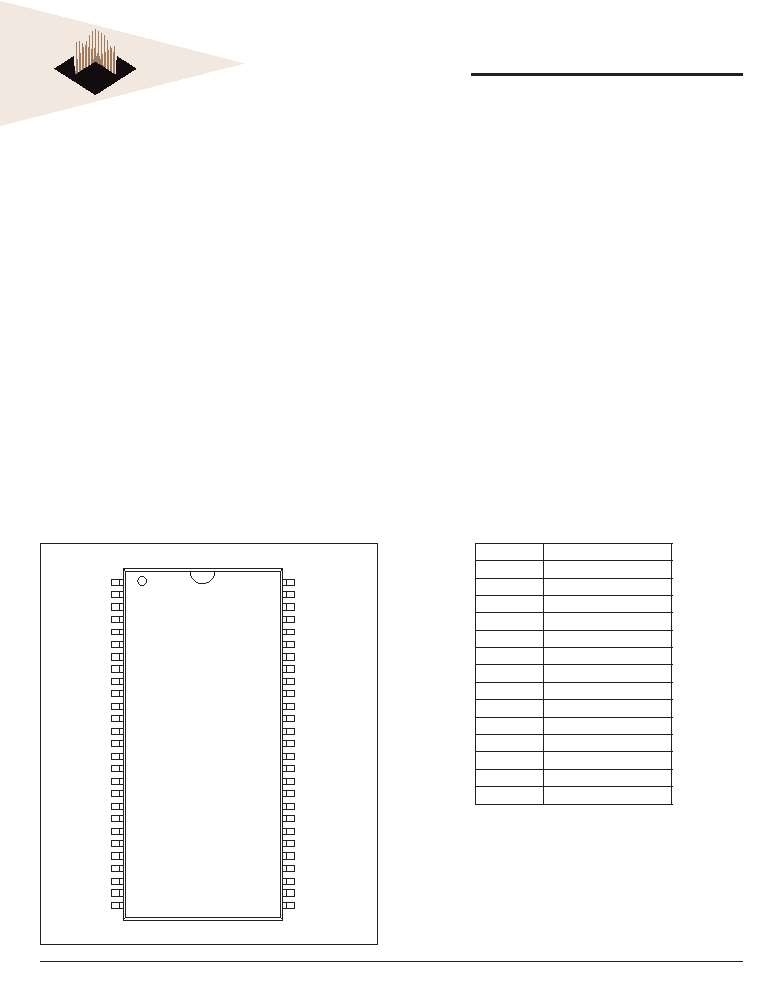
PIN DESCRIPTION
CLK
Clock Input
CKE
Clock Enable
RAS#
Row Address Strobe
CAS#
Column Address Strobe
WE#
Write Enable
CE#
Chip Select
A0-A11
Address Inputs
BA0, BA1
Bank Select Address
DQ0-DQ15
Data Input/Output
L(U)DQM
Data Input/Output Mask
V
CC
Power (+3.3V ±10%)
V
CCQ
Data Output Power
V
SS
Ground
V
SSQ
Data Output Ground
NC
No Connection
PIN CONFIGURATIONS
1
2
3
4
5
6
7
8
9
10
11
12
13
14
15
16
17
18
19
20
21
22
23
24
25
26
27
54
53
52
51
50
49
48
47
46
45
44
43
42
41
40
39
38
37
36
35
34
33
32
31
30
29
28
V
SS
DQ
15
V
SSQ
DQ
14
DQ
13
V
CCQ
DQ
12
DQ
11
V
SSQ
DQ
10
DQ
9
V
CCQ
DQ
8
V
SS
NC/RFU
UDQM
CK
CKE
NC
A
11
A
9
A
8
A
7
A
6
A
5
A
4
V
SS
V
CC
DQ
0
V
CCQ
DQ
1
DQ
2
V
SSQ
DQ
3
DQ
4
V
CCQ
DQ
5
DQ
6
V
SSQ
DQ
7
V
CC
LDQM
WE#
CAS#
RAS#
CE#
BA
0
BA
1
A
10
/AP
A
0
A
1
A
2
A
3
V
CC
TERMINAL
CONNECTIONS
(T
OP
VEIW)

WED416S8030A-SI
2
White Electronic Designs Corporation ∑ (602) 437-1520 ∑ www.wedc.com
White Electronic Designs
October 2004
Rev. 4
White Electronic Designs Corp. reserves the right to change products or specifi cations without notice.
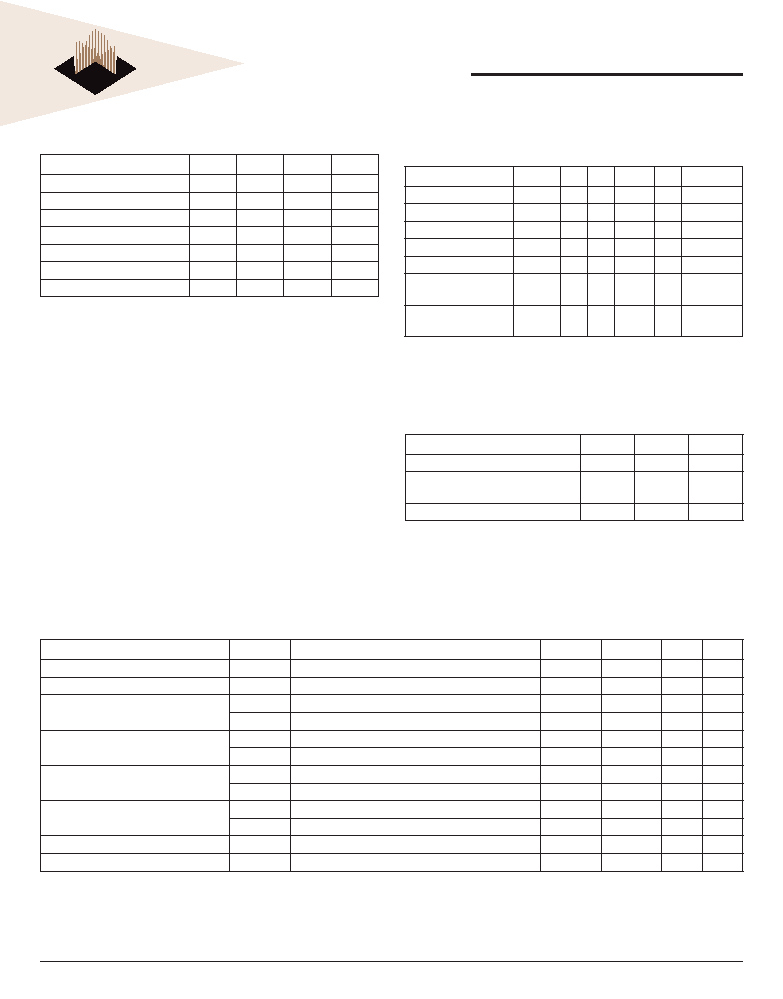
Symbol
Type
Signal
Polarity
Function
CK
Input
Pulse
Positive Edge
The system clock input. All of the SDRAM inputs are sampled on the rising edge of the clock.
CKE
Input
Level
Active High
Activates the CK signal when high and deactivates the CK signal when low. By deactivating
the clock, CKE low initiates the Power Down mode, Suspend mode, or the Self Refresh mode.
CE#
Input
Pulse
Active Low
CE# disable or enable device operation by masking or enabling all inputs except CK, CKE
and DQM.
RAS#,
CAS#, WE#
Input
Pulse
Active Low
When sampled at the positive rising edge of the clock, CAS#, RAS#, and WE# defi ne the
operation to be WE executed by the SDRAM.
BA0, BA1
Input
Level
-
Selects which SDRAM bank is to be active.
A0-11,
A10/AP
Input
Level
-
During a Bank Activate command cycle, A0-11 defi nes the row address (RA0-11) when
sampled at the rising clock edge.
During a Read or Write command cycle, A0-8 defi nes the column address (CA0-8) when
sampled at the rising clock edge. In addition to the row address, A10/AP is used to invoke
Autoprecharge operation at the end of the Burst Read or Write cycle. If A10/AP is high,
autoprecharge is selected and BA0, BA1 defi nes the bank to be precharged . If A10/AP is low,
autoprecharge is disabled. During a Precharge command cycle, A10/AP is used in conjunction
with BA0, BA1 to control which bank(s) to precharge. If A10/AP is high, all banks will be
precharged regardless of the state of BA0, BA1. If A10/AP is low, then BA0, BA1 is used to
defi ne which bank to precharge.
DQ0-15
Input/Output
Level
-
Data Input/Output are multiplexed on the same pins.
L(U)DQM
Input
Pulse
Mask Active High
The Data Input/Output mask places the DQ buffers in a high impedance state when sampled
high. In Read mode, DQM has a latency of two clock cycles and controls the output buffers
like an output enable. In Write mode, DQM has a latency of zero and operates as a word
mask by allowing input data to be written if it is low but blocks the Write operation if DQM is
high.
V
CC
, V
SS
Supply
Power and ground for the input buffers and the core logic.
V
CCQ,
V
SSQ
Supply
Isolated power and ground for the output buffers to improve noise immunity.
INPUT/OUTPUT FUNCTIONAL DESCRIPTION
WED416S8030A-SI
3
White Electronic Designs Corporation ∑ (602) 437-1520 ∑ www.wedc.com
White Electronic Designs
October 2004
Rev. 4
White Electronic Designs Corp. reserves the right to change products or specifi cations without notice.
ABSOLUTE MAXIMUM RATINGS
Parameter
Symbol
Min
Max
Unit
Power Supply Voltage
V
CC
-1.0
+4.6
V
Input Voltage
V
IN
-1.0
+4.6
V
Output Voltage
V
OUT
-1.0
+4.6
V
Operating Temperature
T
OPR
-40
+85
∞C
Storage Temperature
T
STG
-55
+125
∞C
Power Disspation
P
D
1.0
W
Short Circuit Output Current
I
OS
50
mA
Stress greater than those listed under "Absolute Maximum Ratings" may cause
permanent damage to the device. This is a stress rating only and functional operation
of the device at these or any other conditions greater than those indicated in the
operational sections of this specifi cation is not implied. Exposure to absolute maximum
rating conditions for extended periods may affect reliability.
Recommended Operating Conditions
Voltage Referenced to: V
SS
= 0V, -40∞C T
A
+85∞C
Parameter
Symbol Min Typ
Max
Unit
Notes
Supply Voltage
V
CC
3.0
3.3
3.6
V
Input High Voltage
V
IH
2.0
3.0 V
CC
+0.3
V
Input Low Voltage
V
IL
-0.3
--
+0.8
V
Output High Voltage
V
OH
2.4
---
--
V
(I
OH
=-2mA)
Output Low Voltage
V
OL
--
--
0.4
V
(I
OL
=2mA)
Input Leakage
Voltage
I
IL
-5
--
5
µA
Output Leakage
Voltage
I
OL
-5
--
5
µA
Capacitance
T
A
= 25∞C, f = 1MHz, V
CC
= 3.0V to 3.6V
Parameter
Symbol
Max
Unit
Input Capacitance (A0-11, BA0-1)
C
I1
4
pF
Input Capacitance (CK, CKE, RAS#,
CAS# WE#, CE#, L(U)DQM)
C
I2
4
pF
Input/Output Capacitance (DQ0-15)
C
OUT
5
pF
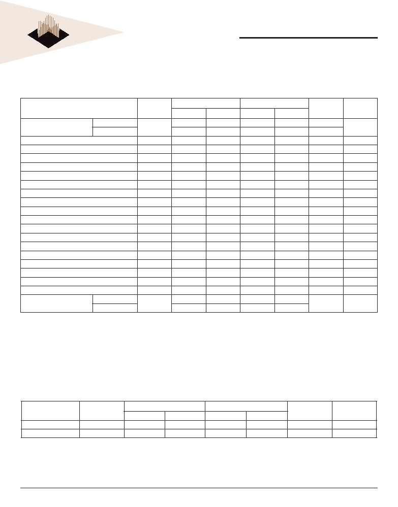
OPERATING CURRENT CHARACTERISTICS
V
CC
= 3.3V, = -40∞C T
A
+85∞C
Parameter
Symbol
Test Conditions
-10
-12
Units
Notes
Operating Current (One Bank Active)
I
CC1
Burst Length = 1, t
RC
t
RC
=min
140
125
mA
1
Operating Current (Burst Mode)
I
CC4
Page Burst, 2 banks active, t
CCD
= 2 clocks
200
165
mA
1
Precharge Standby Current in Power
Down Mode
I
CC2P
CKE
V
IL
(MAX), t
CC
= 15ns
2
2
mA
I
CC2PS
CKE, CK
V
IL
(MAX), t
CC
=
, Input Stable
2
2
mA
Precharge Standby Current in Non-
Power Down Mode
I
CC1N
CKE = V
IH
, t
CC
= 15ns. Input Change every 30ns
50
50
mA
I
CC1NS
CKE
V
IH
(MIN), t
CC
=
, No Input Change
35
35
mA
Active Standby Current in Non-Power
Down Mode
I
CC3P
CKE
V
IL
(MAX), t
CC
= 15ns
12
12
mA
I
CC3PS
CKE
V
IL
(MAX), t
CC
=
12
12
mA
Active Standby Current in Power Down
Mode
I
CC2N
CKE = V
IH
, t
CC
= 15ns, Input Change every 30ns
30
30
mA
I
CC2NS
CKE
V
IH
(MIN), t
CC
=
, No Input Change
20
20
mA
Refresh Current
I
CC5
t
RC
t
RC
(Min)
210
210
mA
2
Self Refresh Current
I
CC6
CKE
0.2V
3
3
mA
NOTE:
1.
Measured with outputs open.
2.
Refresh period is 64ms.
WED416S8030A-SI
4
White Electronic Designs Corporation ∑ (602) 437-1520 ∑ www.wedc.com
White Electronic Designs
October 2004
Rev. 4
White Electronic Designs Corp. reserves the right to change products or specifi cations without notice.
OPERATING AC PARAMETERS
V
CC
= 3.3V, = -40∞C T
A
+85∞C
Parameter
Symbol
-10
-12
Units
Notes
Min
Max
Min
Max
Clock Cycle Time
CAS latency = 3
t
CC
10
1000
12
1000
ns
1
CAS latency = 2
13
1000
15
1000
ns
Clock to Valid Output Delay
t
SAC
7
8
ns
1, 2
Output Dta Hold Time
t
OH
3
3
ns
2
Clock High Pulse Width
t
CH
3.5
4.0
ns
3
Clock Low Pulse Width
t
CL
3.5
4.0
ns
3
Input Setup Time
t
SS
2.5
3
ns
3
Input Hold Time
t
SH
1
1
ns
3
Clock to Output in Low-Z
t
SLZ
1
1
ns
2
Clock to Output in High-Z
t
SHZ
7
8
ns
Row Active to Row Active Delay
t
RRD
20
24
ns
4
RAS# to CAS# Delay
t
RCD
24
26
ns
4
Row Precharge Time
t
RP
24
26
ns
4
Row Active Time
t
RAS
50
100,000
60
100,000
ns
4
Row Cycle Time-Operation
t
RC
80
90
ns
4
Row Cycle Time-Auto Refresh
t
RFC
80
90
ns
4, 8
Last Data In to New Column Address Delay
t
CDL
1
1
CK
5
Last Data In to Row Precharge
t
RDL
1
1
CK
5
Last Data In to Burst Stop
t
BDL
1
1
CK
5
Colunm Address to Column Address Delay
t
CCD
1
1
CK
6
Number of Valid Output Data
CAS latency = 3
2
2
ea
7
CAS latency = 2
1
1
NOTES:
1. Parameters depend on programmed CAS latency.
2. If clock rise time is longer than 1ns, (t
RISE
/2 - 0.5ns) should be added to the parameter.
3. Assumed input
RISE
and fall time = 1ns. If t
RISE
& t
FALL
are longer than 1ns, [(t
RISE
+ t
FALL
)/2-1ns] should be added to the parameter.
4. The minimum number of clock cycles required is determined by dividing the minimum time required by the clock cycle time and then rounding up to the next higher integer.
5. Minimum delay is required to complete write.
6. All devices allow every cycle column address changes.
7. In case of row precharge interrupt, auto precharge and read burst stop.
8.
A new command may be given t
RFC
after self refresh exit.
AC CHARACTERISTICS
REFRESH CYCLE PARAMETERS
Parameter
Symbol
-10
-12
Units
Notes
Min
Max
Min
Max
Refresh Period
t
REF
-
64
-
64
ms
1, 2
Self Refresh Exit Time
t
SREX
t
RFC
-
t
RFC
-
ns
3
NOTES:
1. 4096 cycles.
2. Any time that the Refresh Period has been exceeded, a minimum of two Auto (CBR) Refresh commands must be given to "wake-up" the device.
3. The self refresh is exited by restarting the external clock and then asserting CKE high. This must be followed by NOPs for a minimum time of t
RFC
before the SDRAM reaches idle
state to begin normal operation.
WED416S8030A-SI
5
White Electronic Designs Corporation ∑ (602) 437-1520 ∑ www.wedc.com
White Electronic Designs
October 2004
Rev. 4
White Electronic Designs Corp. reserves the right to change products or specifi cations without notice.
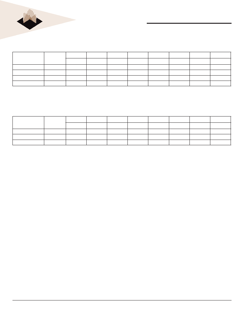
CLOCK FREQUENCY AND LATENCY PARAMETERS = 100MHz
(UNITS = NUMBER OF CLOCKS)
Frequency
CAS
Latency
t
RC
t
RAS
t
RP
t
RRD
t
RCD
t
CCD
t
CDL
t
RDL
80ns
50ns
24ns
20ns
24ns
10ns
10ns
10ns
100MHz (10.0ns)
3
8
5
3
2
3
1
1
1
83MHz (12.0ns)
3
7
5
2
2
2
1
1
1
75MHz (12.0ns)
2
6
4
2
2
2
1
1
1
66MHz (15.0ns)
2
6
4
2
2
2
1
1
1
CLOCK FREQUENCY AND LATENCY PARAMETERS = 83MHz
(UNITS = NUMBER OF CLOCKS)
Frequency
CAS
Latency
t
RC
t
RAS
t
RP
t
RRD
t
RCD
t
CCD
t
CDL
t
RDL
90ns
60ns
26ns
24ns
26ns
12ns
12ns
12ns
83MHz (12ns)
3
8
5
3
2
3
1
1
1
75MHz (12ns)
3
7
5
2
2
2
1
1
1
66MHz (15ns)
2
6
4
2
2
2
1
1
1