
WED48S8030E
1
White Electronic Designs Corporation ∑ (602) 437-1520 ∑ www.wedc.com
White Electronic Designs
White Electronic Designs Corp. reserves the right to change products or specifications without notice.
February, 2002
Rev. 2
2M x 8 Bits x 4 Banks Synchronous DRAM
DESCRIPTION
The WED48S8030E is 67,108,864 bits of synchronous high
data rate DRAM organized as 4 x 2,097,152 words x 8 bits.
Synchronous design allows precise cycle control with the
use of system clock, I/O transactions are possible on every
clock cycle. Range of operating frequencies, programmable
burst lengths and programmable latencies allow the same
device to be useful for a variety of high bandwidth, high
performance memory system applications.
Available in a 54 pin TSOP type II package the
WED48S8030E is tested over the industrial temp range (-
40C to +85C) providing a solution for rugged main memory
applications.
FEATURES
Single 3.3V power supply
Fully Synchronous to positive Clock Edge
Clock Frequency = 125, 100MHz
SDRAM CAS# Latency = 2
Burst Operation
∑Sequential or Interleave
∑Burst length = programmable 1,2,4,8 or full page
∑Burst Read and Write
∑Multiple Burst Read and Single Write
DATA Mask Control
Auto Refresh (CBR) and Self Refresh
∑4096 refresh cycles across 64ms
Automatic and Controlled Precharge Commands
Suspend Mode and Power Down Mode
Industrial Temperature Range
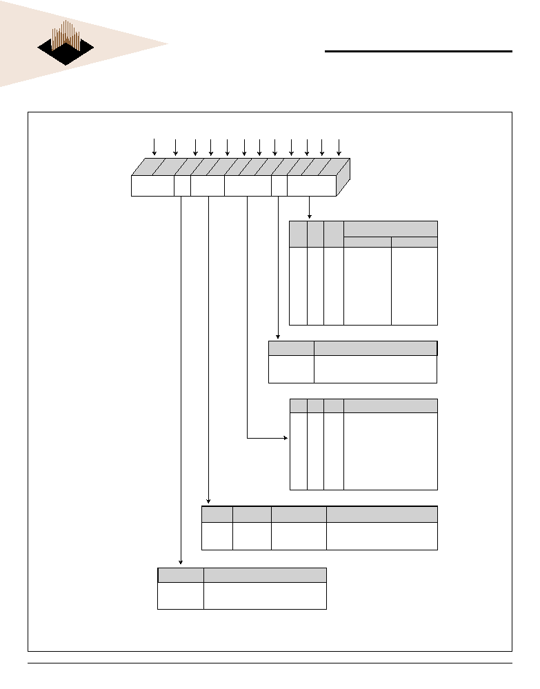
Pin Configuration
FIG. 1
Pin Description
A
0-11
Address Inputs
BA
0
, BA
1
Bank Select Addresses
CE#
Chip Select
WE#
Write Enable
CK
Clock Input
CKE
Clock Enable
DQ
0-7
Data Input/Output
DQM
Data Input/Output Mask
RAS#
Row Address Strobe
CAS#
Column Address Strobe
V
CC
Power (3.3V)
V
CCQ
Data Output Power
V
SS
Ground
V
SSQ
Data Output Ground
NC
No Connection
V
SS
DQ7
V
SSQ
NC
DQ6
V
CCQ
NC
DQ5
V
SSQ
NC
DQ4
V
CCQ
NC
V
SS
NC/RFU
DQM
CK
CKE
NC
A11
A9
A8
A7
A6
A5
A4
V
SS
V
CC
DQ0
V
CCQ
NC
DQ1
V
SSQ
NC
DQ2
V
CCQ
NC
DQ3
V
SSQ
NC
V
CC
NC
WE#
CAS#
RAS#
CE#
BA0
BA1
A10/AP
A0
A1
A2
A3
V
CC
1
2
3
4
5
6
7
8
9
10
11
12
13
14
15
16
17
18
19
20
21
22
23
24
25
26
27
54
53
52
51
50
49
48
47
46
45
44
43
42
41
40
39
38
37
36
35
34
33
32
31
30
29
28
TERMINAL
CONNECTIONS
(T
OP
VIEW)
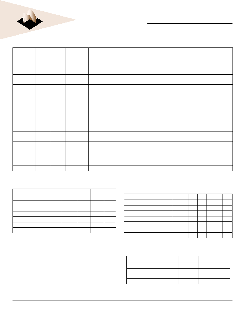
WED48S8030E
2
White Electronic Designs Corporation ∑ (602) 437-1520 ∑ www.wedc.com
White Electronic Designs
White Electronic Designs Corp. reserves the right to change products or specifications without notice.
February, 2002
Rev. 2
INPUT/OUTPUT FUNCTIONAL DESCRIPTION
Symbol
Type
Signal
Polarity
Function
CK
Input
Pulse
Positive Edge The system clock input. All of the SDRAM inputs are sampled on the rising edge of the clock.
CKE
Input
Level
Active High
Activates the CK signal when high and deactivates the CK signal when low. By deactivating the clock,
CKE low initiates the Power Down mode, Suspend mode, or the Self Refresh mode.
CE#
Input
Pulse
Active Low
CE# disable or enable device operation by masking or enabling all inputs except CK, CKE and DQM.
RAS#, CAS#
WE#
Input
Pulse
Active Low
When sampled at the positive rising edge of the clock, CAS#, RAS#, and WE# define the operation to
be executed by the SDRAM.
BA0,BA1
Input
Level
--
Selects which SDRAM bank is to be active.
A0-11,
A10/AP
Input
Level
--
During a Bank Activate command cycle, A0-11 defines the row address (RA0-11) when sampled at the
rising clock edge. During a Read or Write command cycle, A0-7 defines the column address (CA0-7)
when sampled at the rising clock edge. In addition to the row address, A10/AP is used to invoke
Autoprecharge operation at the end of the Burst Read or Write cycle. If A10/AP is high, autoprecharge
is selected and BA0, BA1 defines the bank to be precharged . If A10/AP is low, autoprecharge is
disabled.
During a Precharge command cycle, A10/AP is used in conjunction with BA0, BA1 to control which
bank(s) to precharge. If A10/AP is high, all banks will be precharged regardless of the state of BA0,
BA1. If A10/AP is low, then BA0, BA1 is used to define which bank to precharge.
DQ0-15
Input/
Output
Level
--
Data Input/Output are multiplexed on the same pins
DQM
Input
Pulse
Mask
Active High
The Data Input/Output mask places the DQ buffers in a high impedance state when sampled high.
In Read mode, DQM has a latency of two clock cycles and controls the output buffers like an output
enable. In Write mode, DQM has a latency of zero and operates as a word mask by allowing input data
to be written if it is low but blocks the Write operation if DQM is high.
V
CC
, V
SS
Supply
Power and ground for the input buffers and the core logic.
V
CCQ
, V
SSQ
Supply
Isolated power and ground for the output buffers to improve noise immunity.
Recommended DC Operating Conditions
(Voltage Referenced to: V
SS
= 0V, T
A
= 40∞C to +85∞C)
Absolute Maximum Ratings
Parameter
Symbol Min Typ
Max
Unit
Supply Voltage
V
CC
3.0 3.3
3.6
V
Input High Voltage
V
IH
2.0 3.0 V
CC
+0.3
V
Input Low Voltage
V
IL
-0.3 --
0.8
V
Output High Voltage (I
OH
= -2mA)
V
OH
2.4
--
--
V
Output Low Voltage (I
OL
= 2mA)
V
OL
--
--
0.4
V
Input Leakage Voltage
I
IL
-10
--
10
µA
Output Leakage Voltage
I
OL
-10
--
10
µA
Capacitance
(T
A
= 25∞C, f = 1MHz, V
CC
= 3.3V to 3.6V)
Parameter
Symbol
Min
Max
Units
Power Supply Voltage
V
CC
-1.0
+4.6
V
Input Voltage
V
IN
-1.0
+4.6
V
Output Voltage
V
OUT
-1.0
+4.6
V
Operating Temperature
T
OPR
-40
+85
∞C
Storage Temperature
T
STG
-55
+125
∞C
Power Dissipation
P
D
--
1.0
W
Short Circuit Output Current
I
OS
--
50
mA
Stress greater than those listed under "Absolute Maximum Ratings" may cause
permanent damage to the device. This is a stress rating only and functional
operation of the device at these or any other conditions greater than those indicated
in the operational sections of this specification is not implied. Exposure to absolute
maximum rating conditions for extended periods may affect reliability.
Parameter
Symbol
Max
Unit
Input Capacitance
C
I
1
4
pF
Input Capacitance (CK, CKE,
RAS#, CAS#, WE#, CE#, DQM)
C
1
2
4
pF
Input/Output Capacitance (DQ)
C
OUT
5
pF

WED48S8030E
3
White Electronic Designs Corporation ∑ (602) 437-1520 ∑ www.wedc.com
White Electronic Designs
White Electronic Designs Corp. reserves the right to change products or specifications without notice.
February, 2002
Rev. 2
OPERATING CURRENT Characteristics
(V
CC
= 3.3V, T
A
= 40∞C to +85∞C)
Parameter
Symbol Conditions
-8
-10 Units
Operating Current (One Bank Active) (1)
I
CC
1
Burst Length = 1, t
RC
tRC(min)
100
95
mA
Operating Current (Burst Mode) (1)
I
CC
4
Page Burst, 2 banks active, t
CCD
= 2 clocks
160
130
mA
Precharge Standby Current in Power Down Mode
I
CC
2P
CKE V
IL
(max), t
CC
= 15ns
2
2
mA
I
CC
2PS
CKE, CK V
IL
(max), t
CC
= , Inputs Stable
2
2
mA
Precharge Standby Current in Non-Power Down Mode
I
CC
1N
CKE = V
IH
, t
CC
= 15ns, Input Change every 30ns
20
20
mA
I
CC
1NS
CKE V
IH
(min), t
CC
= , No Input Change
10
10
mA
Precharge Standby Current in Power Down Mode
I
CC
3P
CKE V
IL
(max), t
CC
= 15ns
5
5
mA
I
CC
3PS
CKE V
IL
(max), t
CC
=
5
5
mA
Active Standby Current in Non-Power Down Mode
(One Bank Active)
I
CC
3N
CKE = V
IH
, t
CC
= 15ns, Input Change every 30ns
20
20
mA
I
CC
3NS
CKE V
IH
(min), t
CC
= , No Input Change
10
10
mA
Refresh Current (2)
I
CC
5
t
RC
t
RC
(min)
190
175
mA
Self Refresh Current
I
CC
6
CKE 0.2V
2
2
mA
NOTES:
1. Measured with outputs open.
2. Refresh period is 64ms.
WED48S8030E
4
White Electronic Designs Corporation ∑ (602) 437-1520 ∑ www.wedc.com
White Electronic Designs
White Electronic Designs Corp. reserves the right to change products or specifications without notice.
February, 2002
Rev. 2
OPERATING AC PARAMETERS
(Vcc = 3.3V, T
A
= -40∞C to +85∞C)
Parameter
Symbol
-8
-10
Units
Notes
Min
Max
Min
Max
Refresh Period
t
REF
--
64
--
64
ms
1, 2
Self Refresh Exit Time
t
SREX
t
RFC
--
t
RFC
--
ns
3
NOTES:
1.
4096 cycles.
2.
Any time that the Refresh Period has been exceeded, a minimum of two Auto (CBR) Refresh commands must be given to "wake-up" the device.
3.
The self refresh is exited by restarting the external clock and then asserting CKE high. This must be followed by NOPs for a minimum time of t
RFC
before
the SDRAM reaches idle state to begin normal operation.
NOTES:
1.
Parameters depend on programmed CAS# latency.
2.
If clock rise time is longer than 1ns, (t
RISE
/2-0.5)ns should be added to the parameter.
3.
Assumed input rise and fall time = 1ns. If t
RISE
& tfall are longer than 1ns, [(t
RISE
+ t
FALL
)/2]-1ns should be added to the parameter.
4.
The minimum number of clock cycles required is determined by dividing the minimum time required by the clock cycle time and then rounding up to the next higher integer.
5.
Minimum delay is required to complete write.
6.
All devices allow every cycle column address changes.
7. In case of row precharge interrupt, auto precharge and read burst stop.
8.
A new command may be given t
RFC
after self refresh exit.
AC CHARACTERISTICS
Parameter
Symbol
-8
-10
Units
Min
Max
Min
Max
Clock Cycle Time (1)
CAS Latency = 3
t
CC
7.5
1000
10
1000
ns
CAS Latency = 2
t
CC
10
1000
10
1000
Clock to valid Output delay (1,2)
t
SAC
5.4
6
ns
Output Data Hold Time (2)
t
OH
3
3
ns
Clock HIGH Pulse Width (3)
t
CH
2.5
3.5
ns
Clock LOW Pulse Width (3)
t
CL
2.5
3
ns
Input Setup Time (3)
t
SS
1.5
2
ns
Input Hold Time (3)
t
SH
0.8
1
ns
CK to Output Low-Z (2)
t
SLZ
1
1
ns
CK to Output High-Z
t
SHZ
5.4
6
ns
Row Active to Row Active Delay (4)
t
RRD
15
20
ns
RAS# to CAS# Delay (4)
t
RCD
20
20
ns
Row Precharge Time (4)
t
RP
20
20
ns
Row Active Time (4)
t
RAS
45
100,000
50
100,000
ns
Row Cycle Time - Operation (4)
t
RC
65
70
ns
Row Cycle Time - Auto Refresh (4,8)
t
RFC
65
70
ns
Last Data in to New Column Address Delay (5)
t
CDL
1
1
CK
Last Data in to Row Precharge (5)
t
RDL
1
1
CK
Last Data in to Burst Stop (5)
t
BDL
1
1
CK
Column Address to Column Address Delay (6)
t
CCD
1
1
CK
Number of Valid Output Data (7)
CAS Latency = 3
2
2
ea
CAS Latency = 2
1
1
REFRESH CYCLE PARAMETERS
WED48S8030E
5
White Electronic Designs Corporation ∑ (602) 437-1520 ∑ www.wedc.com
White Electronic Designs
White Electronic Designs Corp. reserves the right to change products or specifications without notice.
February, 2002
Rev. 2
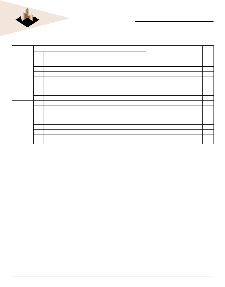
COMMAND TRUTH TABLE
(X = Don't Care, H = Logic High, L = Logic Low)
NOTES:
1.
All of the SDRAM operations are defined by states of CE#, WE#, RAS#, CAS#, and DQM at the positive rising edge of the clock.
2.
Bank Select (BA), if BA = 0 then bank A is selected, if BA = 1 then bank B is selected.
3.
During a Burst Write cycle there is a zero clock delay, for a Burst Read cycle the delay is equal to the CAS# latency.
4.
During normal access mode, CKE is held high and CK is enabled. When it is low, it freezes the internal clock and extends data Read and Write operations. One clock delay is
required for mode entry and exit.
5.
The DQM has two functions for the data DQ Read and Write operations. During a Read cycle, when DQM goes high at a clock timing the data outputs are disabled and become
high impedance after a two clock delay. DQM also provides a data mask function for Write cycles. When it activates, the Write operation at the clock is prohibited (zero clock
latency).
6.
All banks must be precharged before entering the Power Down Mode. The Power Down Mode does not preform any Refresh operations, therefore the device can't remain in this
mode longer than the Refresh period (t
REF
) of the device. One clock delay is required for mode entry and exit.
Function
CKE
CE#
RAS# CAS#
WE#
DQM
BA
A10/AP
A9-0
A12,
A11,
Notes
Previous
Cycle
Current
Cycle
Register
Mode Register Set
H
X
L
L
L
L
X
OP CODE
Refresh
Auto (CBR)
H
H
L
L
L
H
X
X
X
X
Entry Self Refresh
H
L
L
L
L
H
X
X
X
X
Precharge
Single Bank Precharge
H
X
L
L
H
L
X
BA
L
X
2
Precharge all Banks
H
X
L
L
H
L
X
X
H
X
Bank Activate
H
X
L
L
H
H
X
BA
Row Address
2
Write
Auto Precharge Disable
H
X
L
H
L
L
X
BA
L
Column
Address
2
Auto Precharge Enable
H
X
L
H
L
L
X
BA
H
2
Read
Auto Precharge Disable
H
X
L
H
L
L
X
BA
L
Column
Address
2
Auto Precharge Enable
H
X
L
H
L
H
X
BA
H
2
Burst Termination
H
X
L
H
H
L
X
X
X
X
3
No Operation
H
X
L
H
H
H
X
X
X
X
Device Deselect
H
X
H
X
X
X
X
X
X
X
Clock Suspend/Standby Mode
L
X
X
X
X
X
X
X
X
X
4
Data
Write/Output Enable
H
X
X
X
X
X
L
X
X
X
5
Mask/Output Disable
H
X
X
X
X
X
H
X
X
X
5
Power Down
Mode
Entry
X
L
H
X
X
X
X
X
X
X
6
Exit
X
H
H
X
X
X
X
X
X
X
6
WED48S8030E
6
White Electronic Designs Corporation ∑ (602) 437-1520 ∑ www.wedc.com
White Electronic Designs
White Electronic Designs Corp. reserves the right to change products or specifications without notice.
February, 2002
Rev. 2
NOTES:
1.
For the given Current State CKE must be low in the previous cycle.
2.
When CKE has a low to high transition, the clock and other inputs are re-enabled asynchronously. The minimum setup time for CKE (t
CKS
) must be satisfied before any command
other than Exit is issued.
3.
The address inputs (A11-0) depend on the command that is issued. See the Idle State section of the Current State Truth Table for more information.
4.
The Power Down Mode, Self Refresh Mode, and the Mode Register Set can only be entered from the all banks idle state.
5.
Must be a legal command as defined in the Current State Truth Table.
CLOCK ENABLE (CKE
0
) TRUTH TABLE
Current State
CKE
Command
Action
Notes
Previous
Cycle
Current
Cycle
CE#
RAS# CAS# WE# BA0-1
A0-11
Self Refresh
H
X
X
X
X
X
X
X
INVALID
1
L
H
H
X
X
X
X
X
Exit Self Refresh with Device Deselect
2
L
H
L
H
H
H
X
X
Exit Self Refresh with No Operation
2
L
H
L
H
H
L
X
X
ILLEGAL
2
L
H
L
H
L
X
X
X
ILLEGAL
2
L
H
L
L
X
X
X
X
ILLEGAL
2
L
L
X
X
X
X
X
X
Maintain Self Refresh
Power Down
H
X
X
X
X
X
X
X
INVALID
1
L
H
H
X
X
X
X
X
Power Down Mode exit, all banks idle
2
L
H
L
X
X
X
X
X
ILLEGAL
2
H
X
L
H
L
L
X
Maintain Power Down Mode
2
All Banks Idle
H
H
H
X
X
X
Refer to the Idle State section of the
Current State Truth Table
H
H
L
H
X
X
3
H
H
L
L
H
X
H
H
L
L
L
H
X
X
CBR Refresh
H
H
L
L
L
L
OP Code
Mode Register Set
4
H
L
H
X
X
X
Refer to the Idle State section of the
Current State Truth Table
H
L
L
H
X
X
3
H
L
L
L
H
X
H
L
L
L
L
H
X
X
Entry Self Refresh
4
H
H
L
L
L
L
OP Code
Mode Register Set
L
X
X
X
X
X
X
X
Power Down
4
Any State other
than listed above
H
H
X
X
X
X
X
X
Refer to the Operations in the Current
State Truth Table
H
L
X
X
X
X
X
X
Begin Clock Suspend next cycle
5
L
H
X
X
X
X
X
X
Exit Clock Suspend next cycle
L
L
X
X
X
X
X
X
Maintain Clock Suspend
WED48S8030E
7
White Electronic Designs Corporation ∑ (602) 437-1520 ∑ www.wedc.com
White Electronic Designs
White Electronic Designs Corp. reserves the right to change products or specifications without notice.
February, 2002
Rev. 2
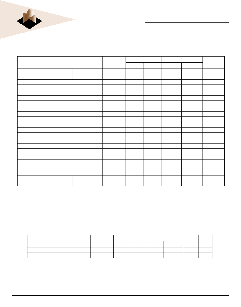
A11 A10 A9
A2 A1 A0
A8 A7 A6 A5 A4 A3
11
10
9
2 1
0
8
7
6
5
4
3
Address Bus
Mode Register (Mx)
Reserved* WB Op Mode CAS Latency BT Burst Length
*Should program
M11, M10 = "0, 0"
to ensure compatability
with future devices.
Burst Length
M2
M3
M8
M9
M7
M6-M0
M1 M0
M3 = 0
M3 = 1
0
0
0
0
1
1
1
1
0
0
1
1
0
0
1
1
0
1
0
1
0
1
0
1
M6 M5 M4
0
0
0
0
1
1
1
1
0
0
1
1
0
0
1
1
0
1
0
1
0
1
0
1
1
2
4
8
1
2
4
8
Reserved
Reserved
Reserved
Full Page
Reserved
Reserved
Reserved
Reserved
Reserved
Reserved
Reserved
Reserved
RRserved
Reserved
Burst Type
0
1
0
1
Sequential
Interleaved
CAS Latency
2
3
0
0
Defined
Operating Mode
Standard Operation
All other states reserved
Write Burst Mode
Programmed Burst Length
Single Location Access
MODE REGISTER SET TABLE

WED48S8030E
8
White Electronic Designs Corporation ∑ (602) 437-1520 ∑ www.wedc.com
White Electronic Designs
White Electronic Designs Corp. reserves the right to change products or specifications without notice.
February, 2002
Rev. 2
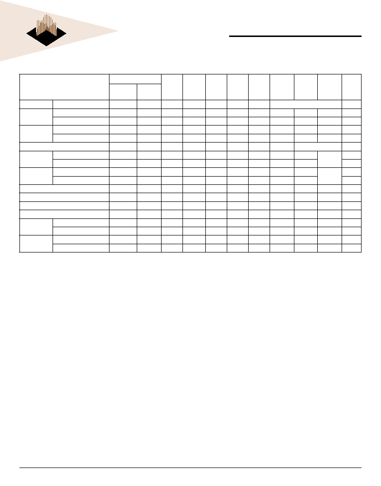
CURRENT STATE TRUTH TABLE
Current State
Command
Action
Notes
CE# RAS# CAS#
WE#
BA0-1
A11, A10/AP-A0
Description
Idle
L
L
L
L
OP Code
Mode Register Set
Set the Mode Register
2
L
L
L
H
X
X
Auto orSelf Refresh
Start Auto orSelf Refresh
2,3
L
L
H
L
X
X
Precharge
No Operation
L
L
H
H
BA
Row Address
Bank Activate
Activate the specified bank and row
L
H
L
L
BA
Column
Write w/o Precharge
ILLEGAL
4
L
H
L
H
BA
Column
Read w/o Precharge
ILLEGAL
2
L
H
H
L
X
X
Burst Termination
No Operation
2
L
H
H
H
X
X
No Operation
No Operation
H
X
X
X
X
X
Device Deselect
No Operation or Power Down
5
Row Active
L
L
L
L
OP Code
Mode Register Set
ILLEGAL
L
L
L
H
X
X
Auto orSelf Refresh
ILLEGAL
L
L
H
L
X
X
Precharge
Precharge
6
L
L
H
H
BA
Row Address
Bank Activate
ILLEGAL
2
L
H
L
L
BA
Column
Write Start
Write; Determine if Auto Precharge
7,8
L
H
L
H
BA
Column
Read Start
Read; Determine if Auto Precharge
7,8
L
H
H
L
X
X
Burst Termination
No Operation
L
H
H
H
X
X
No Operation
No Operation
H
X
X
X
X
X
Device Deselect
No Operation
Read
L
L
L
L
OP Code
Mode Register Set
ILLEGAL
L
L
L
H
X
X
Auto orSelf Refresh
ILLEGAL
L
L
H
L
X
X
Precharge
Terminate Burst; Start the Precharge
L
L
H
H
BA
Row Address
Bank Activate
ILLEGAL
4
L
H
L
L
BA
Column
Write
Terminate Burst; Start the Write cycle
8,9
L
H
L
H
BA
Column
Read
Terminate Burst; Start a new Read cycle
8,9
L
H
H
L
X
X
Burst Termination
Terminate the Burst
L
H
H
H
X
X
No Operation
Continue the Burst
H
X
X
X
X
X
Device Deselect
Continue the Burst
Write
L
L
L
L
OP Code
Mode Register Set
ILLEGAL
L
L
L
H
X
X
Auto orSelf Refresh
ILLEGAL
L
L
H
L
X
X
Precharge
Terminate Burst; Start the Precharge
L
L
H
H
BA
Row Address
Bank Activate
ILLEGAL
4
L
H
L
L
BA
Column
Write
Terminate Burst; Start a new Write cycle
8,9
L
H
L
H
BA
Column
Read
Terminate Burst; Start the Read cycle
8,9
L
H
H
L
X
X
Burst Termination
Terminate the Burst
L
H
H
H
X
X
No Operation
Continue the Burst
H
X
X
X
X
X
Device Deselect
Continue the Burst
Read with
Auto
Precharge
L
L
L
L
OP Code
Mode Register Set
ILLEGAL
L
L
L
H
X
X
Auto orSelf Refresh
ILLEGAL
L
L
H
L
X
X
Precharge
ILLEGAL
4
L
L
H
H
BA
Row Address
Bank Activate
ILLEGAL
4
L
H
L
L
BA
Column
Write
ILLEGAL
L
H
L
H
BA
Column
Read
ILLEGAL
L
H
H
L
X
X
Burst Termination
ILLEGAL
L
H
H
H
X
X
No Operation
Continue the Burst
H
X
X
X
X
X
Device Deselect
Continue the Burst

WED48S8030E
9
White Electronic Designs Corporation ∑ (602) 437-1520 ∑ www.wedc.com
White Electronic Designs
White Electronic Designs Corp. reserves the right to change products or specifications without notice.
February, 2002
Rev. 2
CURRENT STATE TRUTH TABLE (cont.)
Current State
Command
Action
Notes
CE# RAS# CAS# WE# BA0-1 A11, A10/AP-A0
Description
Write with
Auto
Precharge
L
L
L
L
OP Code
Mode Register Set
ILLEGAL
L
L
L
H
X
X
Auto orSelf Refresh
ILLEGAL
L
L
H
L
X
X
Precharge
ILLEGAL
4
L
L
H
H
BA
Row Address
Bank Activate
ILLEGAL
4
L
H
L
L
BA
Column
Write
ILLEGAL
L
H
L
H
BA
Column
Read
ILLEGAL
L
H
H
L
X
X
Burst Termination
ILLEGAL
L
H
H
H
X
X
No Operation
Continue the Burst
H
X
X
X
X
X
Device Deselect
Continue the Burst
Precharging
L
L
L
L
OP Code
Mode Register Set
ILLEGAL
L
L
L
H
X
X
Auto orSelf Refresh
ILLEGAL
L
L
H
L
X
X
Precharge
No Operation; Bank(s) idle after t
RP
L
L
H
H
BA
Row Address
Bank Activate
ILLEGAL
4
L
H
L
L
BA
Column
Write w/o Precharge
ILLEGAL
4
L
H
L
H
BA
Column
Read w/o Precharge
ILLEGAL
4
L
H
H
L
X
X
Burst Termination
No Operation; Bank(s) idle after t
RP
L
H
H
H
X
X
No Operation
No Operation; Bank(s) idle after t
RP
H
X
X
X
X
X
Device Deselect
No Operation; Bank(s) idle after t
RP
Row Activating
L
L
L
L
OP Code
Mode Register Set
ILLEGAL
L
L
L
H
X
X
Auto orSelf Refresh
ILLEGAL
L
L
H
L
X
X
Precharge
ILLEGAL
4
L
L
H
H
BA
Row Address
Bank Activate
ILLEGAL
4,10
L
H
L
L
BA
Column
Write
ILLEGAL
4
L
H
L
H
BA
Column
Read
ILLEGAL
4
L
H
H
L
X
X
Burst Termination
No Operation; Row active after t
RCD
L
H
H
H
X
X
No Operation
No Operation; Row active after t
RCD
H
X
X
X
X
X
Device Deselect
No Operation; Row active after t
RCD
Write
Recovering
L
L
L
L
OP Code
Mode Register Set
ILLEGAL
L
L
L
H
X
X
Auto orSelf Refresh
ILLEGAL
L
L
H
L
X
X
Precharge
ILLEGAL
4
L
L
H
H
BA
Row Address
Bank Activate
ILLEGAL
4
L
H
L
L
BA
Column
Write
Start Write; Determine if Auto Precharge
9
L
H
L
H
BA
Column
Read
Start Read; Determine if Auto Precharge
9
L
H
H
L
X
X
Burst Termination
No Operation; Row active after t
DPL
L
H
H
H
X
X
No Operation
No Operation; Row active after t
DPL
H
X
X
X
X
X
Device Deselect
No Operation; Row active after t
DPL
Write
Recovering
with Auto
Precharge
L
L
L
L
OP Code
Mode Register Set
ILLEGAL
L
L
L
H
X
X
Auto orSelf Refresh
ILLEGAL
L
L
H
L
X
X
Precharge
ILLEGAL
4
L
L
H
H
BA
Row Address
Bank Activate
ILLEGAL
4
L
H
L
L
BA
Column
Write
ILLEGAL
4,9
L
H
L
H
BA
Column
Read
ILLEGAL
4,9
L
H
H
L
X
X
Burst Termination
No Operation; Precharge after t
DPL
L
H
H
H
X
X
No Operation
No Operation; Precharge after t
DPL
H
X
X
X
X
X
Device Deselect
No Operation; Precharge after t
DPL
WED48S8030E
10
White Electronic Designs Corporation ∑ (602) 437-1520 ∑ www.wedc.com
White Electronic Designs
White Electronic Designs Corp. reserves the right to change products or specifications without notice.
February, 2002
Rev. 2
NOTES:
1.
CKE is assumed to be active (high) in the previous cycle for all entries. The Current State is the state of the bank that the command is being applied to.
2.
Both Banks must be idle otherwise it is an illegal action.
3.
If CKE is active (high) the SDRAM starts the Auto (CBR) Refresh operation, if CKE is inactive (low) then the Self Refresh mode is entered.
4.
The Current State refers only refers to one of the banks, if BA selects this bank then the action is illegal. If BA selects the bank not being referenced by the Current State then the
action may be legal depending on the state of that bank.
5.
If CKE is inactive (low) than the Power Down mode is entered, otherwise there is a No Operation.
6.
The minimum and maximum Active time (t
RAS#
) must be satisfied.
7.
The RAS# to CAS# Delay (t
RCD
) must occur before the command is given.
8.
Address A10 is used to determine if the Auto Precharge function is activated.
9.
The command must satisfy any bus contention, bus turn around, and/or write recovery requirements.
10. The command is illegal if the minimum bank to bank delay time (t
RRD
) is not satisfied.
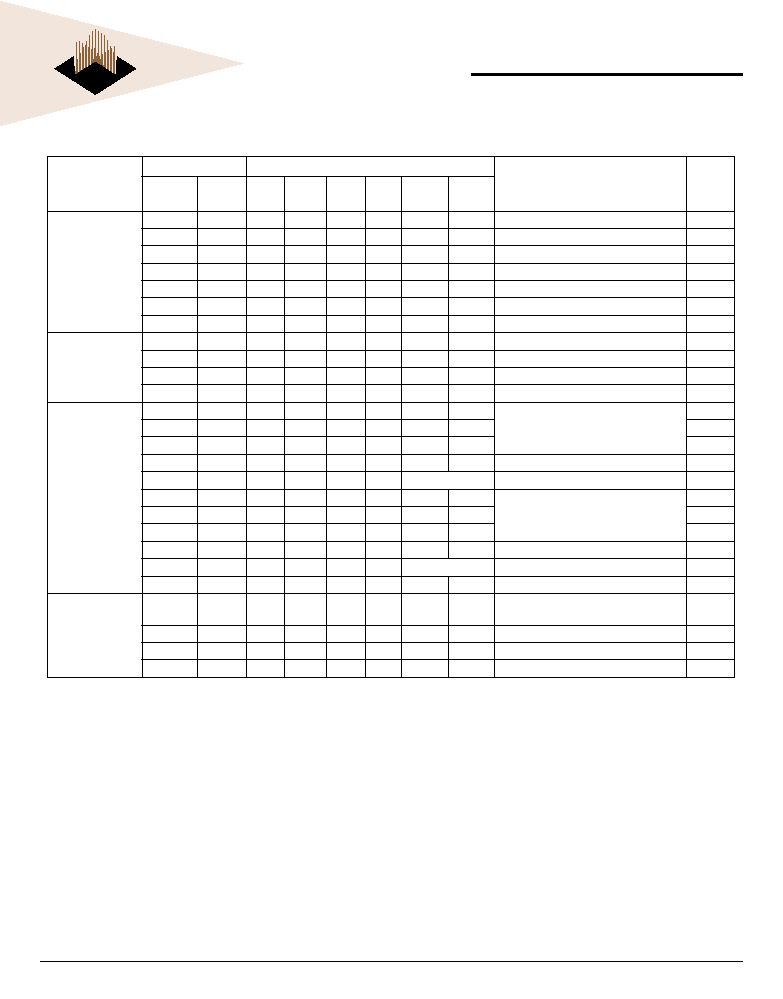
CURRENT STATE TRUTH TABLE (cont.)
Current State
Command
Action
Notes
CE# RAS# CAS# WE# BA0-1 A11, A10/AP-A0
Description
Refreshing
L
L
L
L
OP Code
Mode Register Set
ILLEGAL
L
L
L
H
X
X
Auto orSelf Refresh
ILLEGAL
L
L
H
L
X
X
Precharge
ILLEGAL
L
L
H
H
BA
Row Address
Bank Activate
ILLEGAL
L
H
L
L
BA
Column
Write
ILLEGAL
L
H
L
H
BA
Column
Read
ILLEGAL
L
H
H
L
X
X
Burst Termination
No Operation; Idle after t
RC
L
H
H
H
X
X
No Operation
No Operation; Idle after t
RC
H
X
X
X
X
X
Device Deselect
No Operation; Idle after t
RC
Mode Register
Accessing
L
L
L
L
OP Code
Mode Register Set
ILLEGAL
L
L
L
H
X
X
Auto orSelf Refresh
ILLEGAL
L
L
H
L
X
X
Precharge
ILLEGAL
L
L
H
H
BA
Row Address
Bank Activate
ILLEGAL
L
H
L
L
BA
Column
Write
ILLEGAL
L
H
L
H
BA
Column
Read
ILLEGAL
L
H
H
L
X
X
Burst Termination
ILLEGAL
L
H
H
H
X
X
No Operation
No Operation; Idle after two clock cycles
H
X
X
X
X
X
Device Deselect
No Operation; Idle after two clock cycles
WED48S8030E
11
White Electronic Designs Corporation ∑ (602) 437-1520 ∑ www.wedc.com
White Electronic Designs
White Electronic Designs Corp. reserves the right to change products or specifications without notice.
February, 2002
Rev. 2
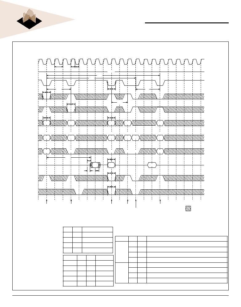
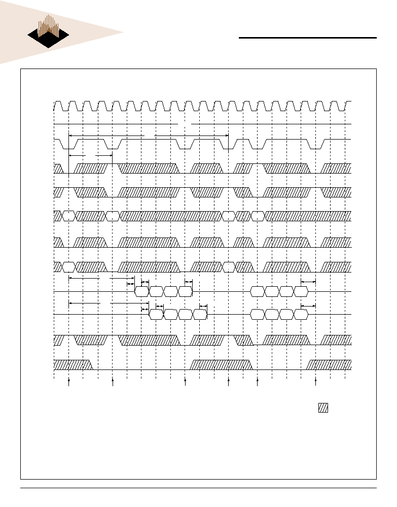
FIG. 2 SINGLE BIT READ-WRITE CYCLE (SAME PAGE) @CAS# LATENCY=3,
BURST LENGTH=1
RAS#
CAS#
ADDR
BA
DQM
t
SS
t
SH
A
10
/AP
CKE
CLOCK
CE#
Cb
Cc
Rb
Ca
Ra
t
SH
DQ
Row Active
Precharge
Read
Write
Read
Row Active
Db
Qc
WE#
0
1
2
3
4
5
6
7
8
9
10
11
12
13
14
15
16
17
18
19
HIGH
t
SS
t
SH
t
RCD
t
RP
t
RAS
t
RCD
t
SS
t
SH
t
SS
BS
BS
BS
BS
BS
Note 3
Note 3
Note 4
Rb
Note 3
Note 2, 3
Note 2, 3
Note 2
Note 4
Note 2, 3
Ra
BS
Qa
t
SH
t
SS
t
OH
t
SAC
t
SLZ
t
SS
t
SH
t
SS
t
SH
t
RAC
t
SS
t
SH
t
CCD
t
CH
t
CL
t
CC
DON'T CARE
Note 2
NOTES:
1.
All input except CKE & DQM can
be don't care when CE# is high at
the CK high going edge.
2.
Bank active & read/write are
controlled by BA0~BA1.
BA0 BA1 Active & Read/Write
0
0
Bank A
0
1
Bank B
1
0
Bank C
1
1
Bank D
A10/AP BA0 BA1 Precharge
0
0
0
Bank A
0
0
1
Bank B
0
1
0
Bank C
0
1
1
Bank D
1
x
x
All Banks
4.
A10/AP and BA0-BA1 control
bank precharge when precharge
command is asserted.
3.
Enable and disable auto precharge function are controlled by A10/AP in read/ write
command.
A10/AP BA0 BA1 Operation
0
0
0
Distribute auto precharge, leave bank A active at end of burst
0
1
Disable auto precharge, leave bank B active at end of burst
1
0
Disable auto precharge, leave bank C active at end of burst
1
1
Disable auto precharge, leave bank D active at end of burst
1
0
0
Enable auto precharge, precharge bank A at end of burst
0
1
Enable auto precharge, precharge bank B at end of burst
1
0
Enable auto precharge, precharge bank C at end of burst
1
1
Enable auto precharge, precharge bank D at end of burst
WED48S8030E
12
White Electronic Designs Corporation ∑ (602) 437-1520 ∑ www.wedc.com
White Electronic Designs
White Electronic Designs Corp. reserves the right to change products or specifications without notice.
February, 2002
Rev. 2
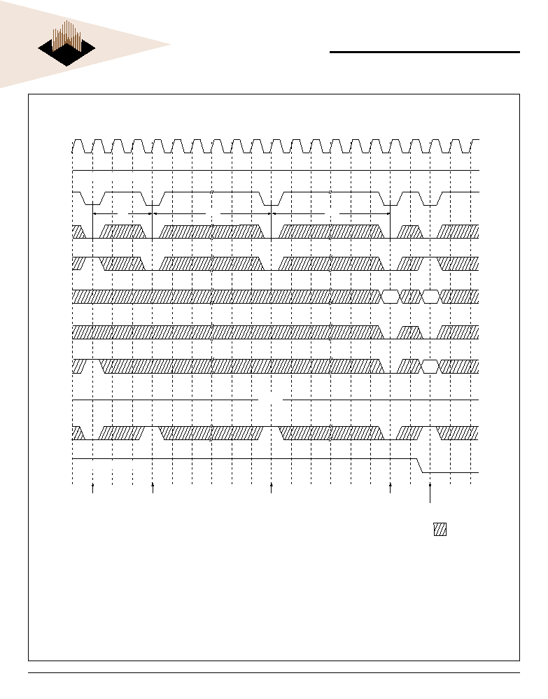
FIG. 3 POWER UP SEQUENCE
RAS#
CAS#
ADDR
BA
DQM
A
10
/AP
CKE
CLOCK
CE#
Key
RAa
DQ
Mode Register Set
Row Active
(A-Bank)
Auto Refresh
Auto Refresh
Precharge
(All Banks)
WE#
0
1
2
3
4
5
6
7
8
9
10
11
12
13
14
15
16
17
18
19
t
RP
RAa
HIGH-Z
t
RFC
t
RFC
High level is necessary
High level is necessary
DON'T CARE
WED48S8030E
13
White Electronic Designs Corporation ∑ (602) 437-1520 ∑ www.wedc.com
White Electronic Designs
White Electronic Designs Corp. reserves the right to change products or specifications without notice.
February, 2002
Rev. 2
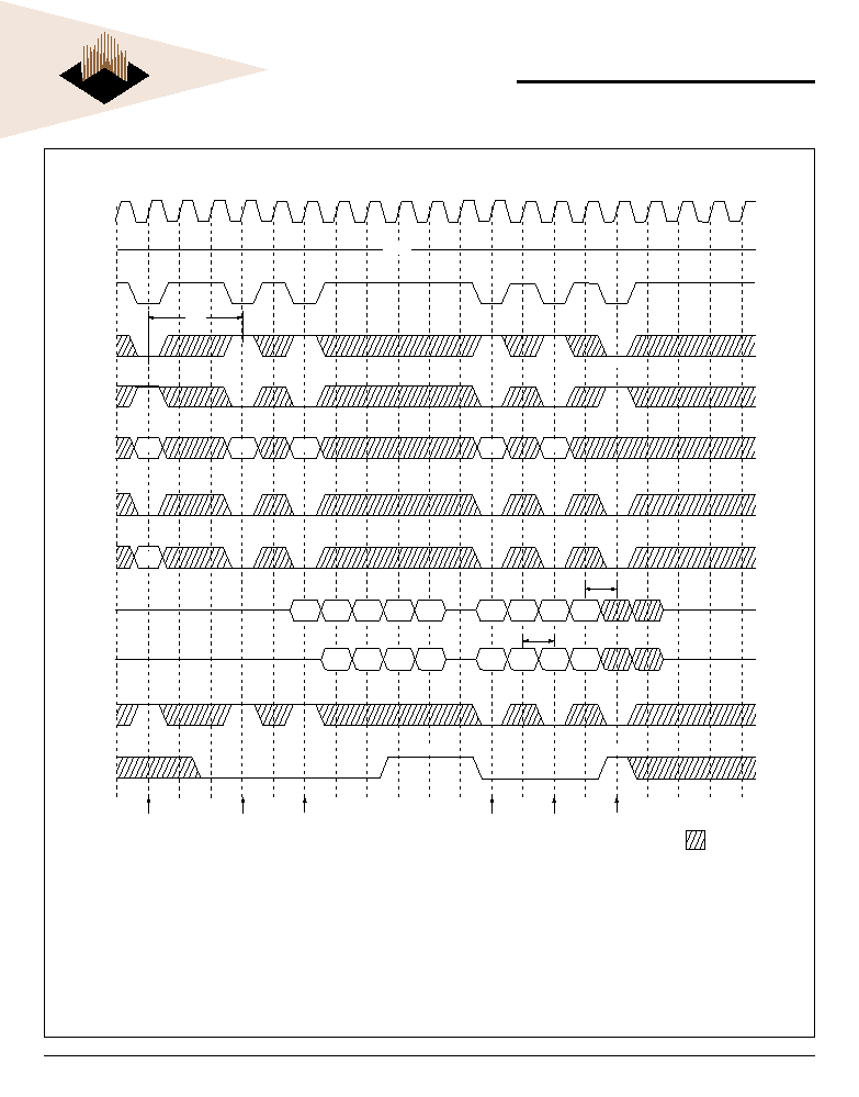
FIG. 4 READ & WRITE CYCLE AT SAME BANK @BURST LENGTH=4
NOTES:
1.
Minimum row cycle times are required to complete internal DRAM operation.
2.
Row precharge can interrupt burst on any cycle. (CAS# Latency - 1) number of valid output data is available after Row precharge. Last valid output will be Hi-
Z(t
SHZ
) after the clock.
3.
Access time from Row active command. t
CC
*(t
RCD
+ CAS# latency - 1) + t
SAC
.
4.
Output will be Hi-Z after the end of burst (1, 2, 4, 8 & full page bit burst).
RAS#
CAS#
ADDR
BA
DQM
A
10
/AP
CKE
CLOCK
CE#
Rb
Cb0
Ca0
Ra
CL = 2
DQ
Row Active
(A-Bank)
Write
(A-Bank)
Precharge
(A-Bank)
Precharge
(A-Bank)
Read
(A-Bank)
Row Active
(A-Bank)
WE#
0
1
2
3
4
5
6
7
8
9
10
11
12
13
14
15
16
17
18
19
HIGH
t
RCD
t
RC
Rb
Note 1
Ra
Qa0
t
SHZ
t
SHZ
t
RDL
t
RDL
t
RAC
t
RAC
Qa1
Qa2
Qa3
Db0
Db1
Db2
Db3
CL = 3
Qa0
Qa1
Qa2
Qa3
Db0
Db1
Db2
Db3
t
SAC
t
SAC
t
OH
t
OH
Note 3
Note 4
Note 4
Note 3
DON'T CARE
Note 2
WED48S8030E
14
White Electronic Designs Corporation ∑ (602) 437-1520 ∑ www.wedc.com
White Electronic Designs
White Electronic Designs Corp. reserves the right to change products or specifications without notice.
February, 2002
Rev. 2
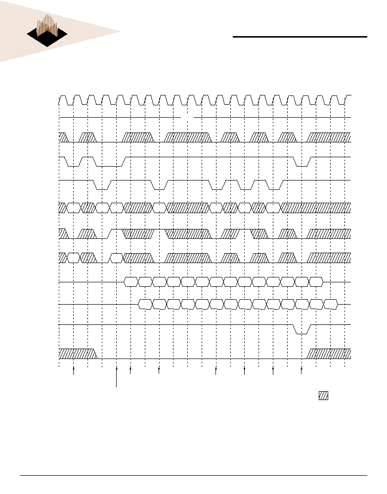
FIG. 5 PAGE READ & WRITE CYCLE AT SAME BANK @ BURST LENGTH=4
RAS#
CAS#
ADDR
BA
DQM
A
10
/AP
CKE
CLOCK
CE#
Cc0
Cd0
Ca0
Ra
CL = 2
DQ
Write
(A-Bank)
Write
(A-Bank)
Read
(A-Bank)
Precharge
(A-Bank)
Read
(A-Bank)
Row Active
(A-Bank)
WE#
0
1
2
3
4
5
6
7
8
9
10
11
12
13
14
15
16
17
18
19
HIGH
t
RCD
Ra
Qa0
t
RDL
t
CDL
Qa1
Qb0
Qb1
Qb2
Dc0
Dc1
Dd0
Dd1
CL = 3
Qa0
Qa1
Qb0
Qb1
Dc0
Dc1
Dd0
Dd1
DON'T CARE
Cb0
Note 2
Note 3
Note 1
NOTES:
1.
To write data before burst read ends, DQM should be asserted three cycles prior to write command to avoid bus contention.
2.
Row precharge will interrupt writing. Last data input, t
RDL
before Row precharge, will be written.
3.
DQM should mask invalid input data on precharge command cycle when asserting precharge before end of burst. Input data after Row precharge cycle
will be masked internally.
WED48S8030E
15
White Electronic Designs Corporation ∑ (602) 437-1520 ∑ www.wedc.com
White Electronic Designs
White Electronic Designs Corp. reserves the right to change products or specifications without notice.
February, 2002
Rev. 2
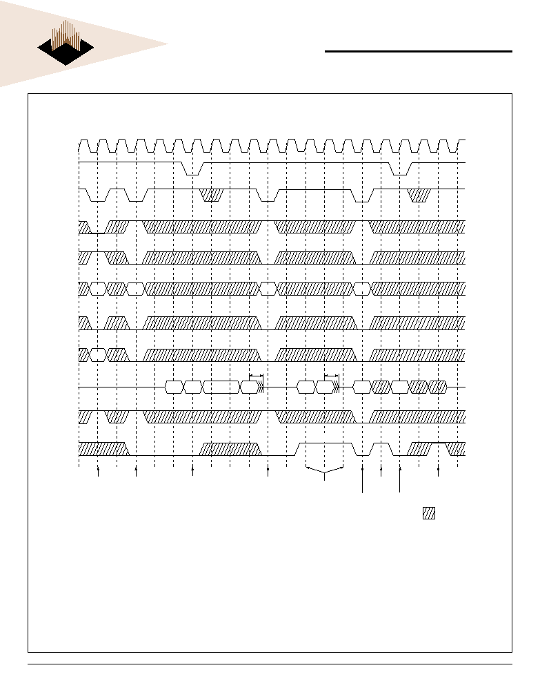
FIG. 6 PAGE READ CYCLE AT DIFFERENT BANK @ BURST LENGTH=4
RAS#
CAS#
ADDR
BA
DQM
A
10
/AP
CKE
CLOCK
CE#
CAc
CBd
CAe
RBb
CAa
RAa
CL = 2
DQ
Read
(A-Bank)
Read
(A-Bank)
Read
(B-Bank)
Row Active
(B-Bank)
Read
(B-Bank)
Precharge
(A-Bank)
Read
(A-Bank)
Row Active
(A-Bank)
WE#
0
1
2
3
4
5
6
7
8
9
10
11
12
13
14
15
16
17
18
19
HIGH
RAa
QAa2
QAa3
QBb0
QBb1
QBb2
QBb3
QAc0
QAc1
QBd0
QBd1 QAe0
QAe1
CL = 3
QAa2
QAa3
QAa0
QAa1
QAa0
QAa1
QBb0
QBb1
QBb3
QBb2
QAc0
QAc1
QBd0 QBd1
QAe0
QAe1
DON'T CARE
CBb
Note 2
Note 1
RBb
NOTES:
1.
CE# can be don't cared when RAS#, CAS# and WE# are high at the clock high going edge.
2.
To interrupt a burst read by row precharge, both the read and the precharge banks must be the same.

WED48S8030E
16
White Electronic Designs Corporation ∑ (602) 437-1520 ∑ www.wedc.com
White Electronic Designs
White Electronic Designs Corp. reserves the right to change products or specifications without notice.
February, 2002
Rev. 2
FIG. 7 PAGE WRITE CYCLE AT DIFFERENT BANK @ BURST LENGTH=4
NOTES:
1.
To interrupt burst write by Row precharge, DQM should be asserted to mask invalid input data.
2.
To interrupt burst write by Row precharge, both the write and the precharge banks must be the same.
RAS#
CAS#
ADDR
BA
DQM
A
10
/AP
CKE
CLOCK
CE#
CAc
CBd
RBb
CAa
RAa
DQ
Write
(A-Bank)
Write
(B-Bank)
Row Active
(B-Bank)
Write
(B-Bank)
Precharge
(Both Banks)
Write
(A-Bank)
Row Active
(A-Bank)
WE#
0
1
2
3
4
5
6
7
8
9
10
11
12
13
14
15
16
17
18
19
HIGH
RAa
DAa3
DBb0
DBb1
DBb2
DBb3
DAc0
DAc1
DBd0
DBd1
DAa1
DAa0
DAa2
DON'T CARE
CBb
Note 2
Note 1
RBb
t
RDL
t
CDL

WED48S8030E
17
White Electronic Designs Corporation ∑ (602) 437-1520 ∑ www.wedc.com
White Electronic Designs
White Electronic Designs Corp. reserves the right to change products or specifications without notice.
February, 2002
Rev. 2
FIG. 8 READ & WRITE CYCLE AT DIFFERENT BANK @ BURST LENGTH=4
NOTE:
1.
t
CDL
should be met to complete write.
RAS#
CAS#
ADDR
BA
DQM
A
10
/AP
CKE
CLOCK
CE#
RAc
CAc
CAa
RBb
RAa
CL = 2
Read
(A-Bank)
Row Active
(A-Bank)
Read
(A-Bank)
Write
(B-Bank)
Precharge
(A-Bank)
Row Active
(B-Bank)
Row Active
(A-Bank)
WE#
0
1
2
3
4
5
6
7
8
9
10
11
12
13
14
15
16
17
18
19
HIGH
RAa
QAa3
DBb0
DBb1
DBb2
DBb3
QAc0
QAc1
QAa1
QAa0
QAa2
DON'T CARE
CBb
Note 1
RAc
RBb
t
CDL
QAc2
CL = 3
DQ
QAa3
DBb0
DBb1
DBb2
DBb3
QAc0
QAc1
QAa1
QAa0
QAa2

WED48S8030E
18
White Electronic Designs Corporation ∑ (602) 437-1520 ∑ www.wedc.com
White Electronic Designs
White Electronic Designs Corp. reserves the right to change products or specifications without notice.
February, 2002
Rev. 2
FIG. 9 READ & WRITE CYCLE WITH AUTO PRECHARGE @ BURST LENGTH=4
NOTE:
1.
t
CDL
should be controlled to meet minimum t
RAS
before internal precharge start. (in the case of Burst Length=1 & 2 and BRSW mode)
RAS#
CAS#
ADDR
BA
DQM
A
10
/AP
CKE
CLOCK
CE#
Cb
Ca
Rb
Ra
CL = 2
Auto Precharge
Start Point
(B-Bank)
Auto Precharge
Start Point
(A-Bank)
Write with
Auto Precharge
(B-Bank)
Read with
Auto Precharge
(A-Bank)
Row Active
(B-Bank)
Row Active
(A-Bank)
WE#
0
1
2
3
4
5
6
7
8
9
10
11
12
13
14
15
16
17
18
19
HIGH
Ra
Qa3
Db0
Db1
Db2
Db3
Qa1
Qa0
Qa2
DON'T CARE
Rb
CL = 3
DQ
Qa3
Db0
Db1
Db2
Db3
Qa1
Qa0
Qa2
WED48S8030E
19
White Electronic Designs Corporation ∑ (602) 437-1520 ∑ www.wedc.com
White Electronic Designs
White Electronic Designs Corp. reserves the right to change products or specifications without notice.
February, 2002
Rev. 2
FIG. 10 CLOCK SUSPENSION & DQM OPERATION CYCLE @ CAS# LATENCY=2,
BURST LENGTH=4
NOTE:
1.
DQM is needed to prevent bus contention.
RAS#
CAS#
ADDR
BA
DQM
A
10
/AP
CKE
CLOCK
CE#
Cb
Cc
Ca
DQ
Read
Read DQM
Write
Write
DQM
Write
DQM
Clock
Suspension
Clock
Suspension
Read
Row Active
WE#
0
1
2
3
4
5
6
7
8
9
10
11
12
13
14
15
16
17
18
19
Ra
Qa0
t
SHZ
t
SHZ
Qa1
Qa2
Qa3
Dc0
Dc2
DON'T CARE
Qb1
Qb1
Ra
Note 1

WED48S8030E
20
White Electronic Designs Corporation ∑ (602) 437-1520 ∑ www.wedc.com
White Electronic Designs
White Electronic Designs Corp. reserves the right to change products or specifications without notice.
February, 2002
Rev. 2
FIG. 11 READ INTERRUPTED BY PRECHARGE COMMAND & READ BURST
STOP @ BURST LENGTH=FULL PAGE
RAS#
CAS#
ADDR
BA
DQM
A
10
/AP
CKE
CLOCK
CE#
CAb
CAa
RAa
CL = 2
Precharge
(A-Bank)
Read
(A-Bank)
Burst Stop
Read
(A-Bank)
Row Active
(A-Bank)
WE#
0
1
2
3
4
5
6
7
8
9
10
11
12
13
14
15
16
17
18
19
HIGH
DON'T CARE
RAa
QAa0
QAa1
QAa2
QAa3
QAa4
QAb1
QAb0
QAb3
QAb2
QAb5
QAb4
CL = 3
DQ
QAa0
QAa1
QAa2
QAa3
QAa4
QAb1
QAb0
QAb3
QAb2
QAb5
QAb4
Note 2
1
1
2
2
NOTES:
1.
At full page mode, burst is end at the end of burst. So auto precharge is possible.
2.
About the valid DQs after burst stop, it is same as the case of RAS# interrupt.
Both cases are illustrated in above timing diagram. See the label 1, 2.
But at burst write, Burst stop and RAS# interrupt should be compared carefully.
Refer to the timing diagram of "Full page write burst stop cycle."
3.
Burst stop is valid at every burst length.
WED48S8030E
21
White Electronic Designs Corporation ∑ (602) 437-1520 ∑ www.wedc.com
White Electronic Designs
White Electronic Designs Corp. reserves the right to change products or specifications without notice.
February, 2002
Rev. 2
FIG. 12 WRITE INTERRUPTED BY PRECHARGE COMMAND & WRITE BURST
STOP CYCLE @ BURST LENGTH=FULL PAGE
NOTES:
1.
At full page mode, burst is end at the end of burst. So auto precharge is possible.
2.
Data-in at the cycle of interrupted by precharge cannot be written into the corresponding memory cell. It is defined by AC parameter of t
RDL
. DQM at write
interrupted by precharge command is needed to prevent invalid write. DQM should mask invalid input data on precharge command cycle when asserting
precharge before end of burst. Input data after Row precharge cycle will be masked internally.
3.
Burst stop is valid at every burst length.
RAS#
CAS#
ADDR
BA
DQM
A
10
/AP
CKE
CLOCK
CE#
CAb
CAa
RAa
DQ
Precharge
(A-Bank)
Write
(A-Bank)
Burst Stop
Write
(A-Bank)
Row Active
(A-Bank)
WE#
0
1
2
3
4
5
6
7
8
9
10
11
12
13
14
15
16
17
18
19
HIGH
DON'T CARE
RAa
DAa0
DAa1
DAa2
DAa3
DAa4
DAb1
DAb0
DAb3
DAb2
DAb5
DAb4
Note 2
t
RDL
t
BDL
WED48S8030E
22
White Electronic Designs Corporation ∑ (602) 437-1520 ∑ www.wedc.com
White Electronic Designs
White Electronic Designs Corp. reserves the right to change products or specifications without notice.
February, 2002
Rev. 2
FIG. 13 BURST READ SINGLE BIT WRITE CYCLE @ BURST LENGTH=2
NOTES:
1.
BRSW mode is enabled by setting As "High" at MRS (Mode Register Set). At the BRSW Mode, the burst length at write is fixed to "1"
regardless of programmed burst length.
2.
When BRSW write command with auto precharge is executed, keep it in mind that t
RAS
should not be violated. Auto precharge is
executed at the burst-end cycle, so in the case of BRSW write command, the next cycle starts the precharge.
RAS#
CAS#
ADDR
BA
DQM
A
10
/AP
CKE
CLOCK
CE#
CBc
CAd
RBb
CAa
RAa
CL = 2
Row Active
(A-Bank)
Read
(A-Bank)
Row Active
(B-Bank)
Write with
Auto Precharge
(B-Bank)
Precharge
(Both Banks)
Write
(A-Bank)
Read with
Auto Precharge
(A-Bank)
Row Active
(A-Bank)
WE#
0
1
2
3
4
5
6
7
8
9
10
11
12
13
14
15
16
17
18
19
HIGH
RAa
QAb0
QAb1
DBc0
QAd0
QAd1
DAa0
DON'T CARE
CAb
Note 2
RBb
RAc
RAc
CL = 3
DQ
QAb0
QAb1
DBc0
QAd0
QAd1
DAa0
Note 1

WED48S8030E
23
White Electronic Designs Corporation ∑ (602) 437-1520 ∑ www.wedc.com
White Electronic Designs
White Electronic Designs Corp. reserves the right to change products or specifications without notice.
February, 2002
Rev. 2
FIG. 14 ACTIVE/PRECHARGE POWER DOWN MODE @ CAS# LATENCY=2,
BURST LENGTH=4
NOTES:
1.
Both banks should be in idle state prior to entering precharge power down mode.
2.
CKE should be set high at least 1 CK + t
SS
prior to Row active command.
3.
Cannot violate minimum refresh specification (64ms).
RAS#
CAS#
ADDR
BA
DQM
A
10
/AP
CKE
CLOCK
CE#
Ra
Ca
DQ
Precharge
Read
Row Active
Precharge
Power-Down
Entry
Precharge
Power-Down
Exit
Active
Power-Down
Entry
Active
Power-Down
Exit
WE#
0
1
2
3
4
5
6
7
8
9
10
11
12
13
14
15
16
17
18
19
Note 3
Note 2
t
SS
DON'T CARE
t
SS
t
SS
t
SHZ
Note 1
Ra
Qa1
Qa0
Qa2
WED48S8030E
24
White Electronic Designs Corporation ∑ (602) 437-1520 ∑ www.wedc.com
White Electronic Designs
White Electronic Designs Corp. reserves the right to change products or specifications without notice.
February, 2002
Rev. 2
FIG. 15 SELF REFRESH ENTRY & EXIT CYCLE
RAS#
CAS#
ADDR
BA
DQM
A
10
/AP
CKE
CLOCK
CE#
DQ
Auto Refresh
Self Refresh Entry
Self Refresh Exit
WE#
0
1
2
3
4
5
6
7
8
9
10
11
12
13
14
15
16
17
18
19
t
SS
DON'T CARE
Note 1
Note 3
Note 4
t
RFC
min
Note 6
Note 5
Note 7
HI-Z
HI-Z
Note 2
NOTES:
TO ENTER SELF REFRESH MODE
1.
CE#, RAS# & CAS# with CKE should be low at the same clock cycle.
2.
After 1 clock cycle, all the inputs including the system clock can be don't care except for CKE.
3.
The device remains in self refresh mode as long as CKE stays "Low." Once the device enters self refresh mode, minimum t
RAS#
is required before exit from
self refresh.
TO EXIT SELF REFRESH MODE
4.
System clock restart and be stable before returning CKE high.
5.
CE# starts from high.
6.
Minimum t
RFC
is required after CKE going high to complete self refresh exit.
7.
4K cycle of burst auto refresh is required before self refresh entry and after self refresh exit if the system uses burst refresh.
WED48S8030E
25
White Electronic Designs Corporation ∑ (602) 437-1520 ∑ www.wedc.com
White Electronic Designs
White Electronic Designs Corp. reserves the right to change products or specifications without notice.
February, 2002
Rev. 2
FIG. 16 MODE REGISTER SET
CYCLE
FIG. 17 AUTO REFRESH CYCLE
RAS#
CAS#
ADDR
DQM
CKE
CLOCK
CE#
Ra
Key
DQ
New Command
New
Command
Auto Refresh
MRS
WE#
0
1
2
3
4
5
6
0
1
2
3
4
5
6
7
8
9
10
DON'T CARE
t
RFC
HI-Z
HI-Z
Note 2
Note 1
Note 3
HIGH
HIGH
NOTES:
Both banks precharge should be completed before Mode Register Set cycle and auto refresh cycle.
MODE REGISTER SET CYCLE
1.
CE#, RAS#, CAS#, & WE# activation at the same clock cycle with address key will set internal
mode register.
2.
Minimum 2 clock cycles should be met before new RAS# activation.
3.
Please refer to Mode Register Set table.
WED48S8030E
26
White Electronic Designs Corporation ∑ (602) 437-1520 ∑ www.wedc.com
White Electronic Designs
White Electronic Designs Corp. reserves the right to change products or specifications without notice.
February, 2002
Rev. 2
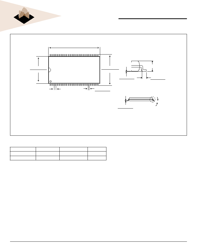
PACKAGE DIMENSION:54 PIN TSOP II
ALL LINEAR DIMENSIONS ARE IN MILLIMETERS AND PARENTHETICALLY IN INCHES
NOTES:
1.
Dimension does not include 0.006 inch Flash each side.
2.
Dimension does not include 0.010 inch Flash each side.
22.35 (0.880)
22.10 (0.870)
Note 1
10.27 (0.405)
10.03 (0.395)
Note 2
0.80 (0.0315)
TYP
0.51 (0.020)
0.25 (0.010)
0.203 (0.008)
0.125 (0.005)
0.15 (0.006)
0.05 (0.002)
0.61 (0.024)
0.41 (0.016)
VIEW A
1.20 (0.047)
MAX
11.96 (0.471)
11.56 (0.455)
SEE VIEW A
0 - 8
ORDERING INFORMATION
Part Number
Organization
Operating Frequency
Package
WED48S8030E8SI
2Mx8bitsx4banks
125MHz
54 TSOP II
WED48S8030E10SI 2Mx8bitsx4banks
100MHz
54 TSOP II
NOTE: This product does not include the prefix "WED" for part marking due to package size constraints.