1
White Electronic Designs Corporation ∑ (602) 437-1520 ∑ www.wedc.com
White Electronic Designs
WED7F324XDNSN
Sept, 2002
Rev. 0A
White Electronic Designs Corp. reserves the right to change products or specifications without notice.
WED7F324DNSN: 4Mx32 80 PIN SIMM
4Mx32 and 2x4mx32 Densities
Based on Intel's Strataflash (J3) family of Flash
Devices
E28F320J3
(32) 128Kb Erase Blocks (Symetrical)
High Performance Interface Async Page Mode Reads
120/25 ns Read Access Time
2.7V - 3.6V V
CC
Operation
128 bit Protection Register;
64 bit Unique Device Identifier
64 bit User Programmable OTP Cells
Common Flash Interface (CFI)
Scaleable Command Set (SCS)
32 byte Write Buffer, 32M Total Erase Cycles
100,000 Erase Cycles per Block
Package
80 pin SIMM
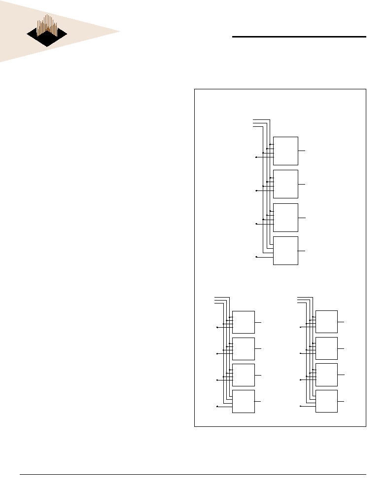
The WED7F324XDNSN and WED7F2324XDNSN are
organized as one and two banks of 4Mx32 respectively.
The modules are based on Intel's E28F320J3, 4Mx8 /
2Mx16 device family. Both modules offer access times
of 120ns.
WED7F2324XDNSN: 2x4Mx32 80 PIN SIMM
FIG. 1 BLOCK DIAGRAMS
A0-A21
E0#
G#
W0#
W1#
W2#
W3#
DQ0-7
DQ8-15
DQ16-23
DQ24-31
4Mx8
4Mx8
4Mx8
4Mx8
A0-A21
E0#
G#
W0#
W1#
W2#
W3#
DQ0-7
DQ8-15
DQ16-23
DQ24-31
4Mx8
4Mx8
4Mx8
4Mx8
FEATURES
DESCRIPTION
4Mx32 / 2x4Mx32; INTEL J3 BASED, FLASH MODULE
A0-A21
E0#
G#
W0#
W1#
W2#
W3#
DQ0-7
DQ8-15
DQ16-23
DQ24-31
4Mx8
4Mx8
4Mx8
4Mx8
2
White Electronic Designs Corporation ∑ (602) 437-1520 ∑ www.wedc.com
White Electronic Designs
WED7F324XDNSN
Sept, 2002
Rev. 0A
White Electronic Designs Corp. reserves the right to change products or specifications without notice.
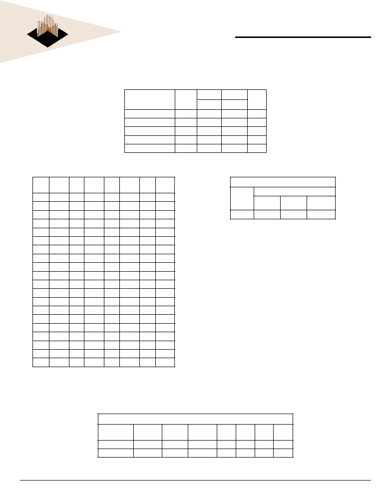
PIN CONFIGURATIONS
CAPACITANCE
(f=1.0MH
Z
, V
IN
= V
CC
or V
SS
)
Parameter
Sym
4Mx32 2x4Mx32 Unit
Max
Max
Address Lines
CA
35
70
pF
Data lines
CDQ
15
30
pF
Chip Enable Lines
CE
40
40
pF
Write Enable Lines
CW
20
20
pF
Output Enable lines
CG
40
80
pF
Pin
#
Pin
Name
Pin
#
Pin
Name
Pin
#
Pin
Name
Pin
#
Pin
Name
1
V
SS
21
NC
41
A11
61
DQ9
2
V
CC
22
NC
42
A10
62
DQ8
3
NC
23
*
43
A9
63
DQ7
4
G#
24
*
44
A8
64
DQ6
5
W0#
25
V
SS
45
A7
65
DQ5
6
W1#
26
DQ29 461
A6
66
DQ4
7
NC
27
DQ30
47
A5
67
DQ3
8
DQ16 28
DQ31
48
A4
68
DQ2
9
DQ17 29
W2#
49
A3
69
DQ1
10
DQ18 30
NC
50
A2
70
DQ0
11
DQ19 31
A21
51
A1
71
NC
12
DQ20 32
A20
52
AO
72
V
CC
13
DQ21 33
A19
53
W3#
73
PD1
14
DQ22 34
A18
54
V
SS
74
PD2
15
DQ23 35
A17
55
DQ15
75
PD3
16
DQ24 36
A16
56
DQ14
76
PD4
17
DQ25 37
A15
57
DQ13
77
PD5
18
DQ26 38
A14
58
DQ12
78
PD6
19
DQ27 39
A13
59
DQ11
79
PD7
20
DQ28 40
A12
60
DQ10
80
V
SS
Module Configurator - Presence Detect Pins
Module
Organization
Device
Density
# of
Device
Module
Capacity
PD1
PD2
PD3
PD4
4Mx32
32Mb
4
16MB
0
1
1
1
8Mx32
32Mb
8
16MB
1
0
1
1
MODULE SPEED VIA PRESENCE DETECT
MODULE CONFIGURATION
* SIMM DENSITY
16 MB PIN 24= E0#
PIN 23= NC
32 MB PIN 24= E0#
PIN 23= E1#
Module Speed Identification
Max
Access
Time
Presence Detect Pin Identification
PD5
PD6
PD7
120ns
0
1
0
3
White Electronic Designs Corporation ∑ (602) 437-1520 ∑ www.wedc.com
White Electronic Designs
WED7F324XDNSN
Sept, 2002
Rev. 0A
White Electronic Designs Corp. reserves the right to change products or specifications without notice.
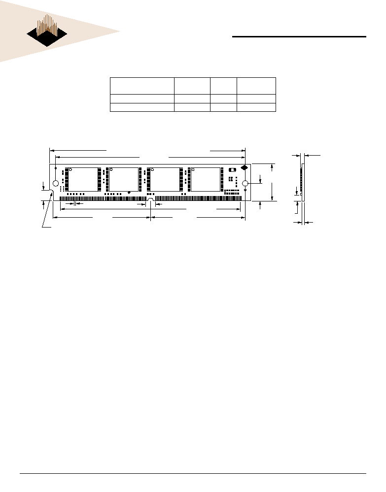
ORDERING INFORMATION
ALL DIMENSION ARE IN INCHES
MECHANICAL PACKAGE: 80 PIN SIMM
4.655 MAX. (SEE NOTE 1)
4.384
.125 DIA (2x)
.250
R. 062 (2x)
2.245
.050 TYP.
.250
2.192
4.150
.400
.850
MAX.
.120
MAX.
.125
MIN.
.050 ± .004
.003
WED
253
P1
Part Number
Organization
Speed
(ns)
Package
WED7F324XDNSN12C
4M x 32
120
80 PIN SIMM
WED7F2324XDNSN12C
2 x 4M x 32
120
80 PIN SIMM