
1
White Electronic Designs Corporation ∑ (602) 437-1520 ∑ www.wedc.com
White Electronic Designs
WED9LAPC2B16P8BC
November 2001
Rev. 1
White Electronic Designs Corp. reserves the right to change products or specifi cations without notice.
DESCRIPTION
The WED9LAPC2B16P8BC is a 3.3V, 4M x 32 Synchronous
DRAM and a 2M x 8 Synchronous DRAM array packaged
in a 14mm x 22mm 153 lead BGA.
The WED9LAPC2B16P8BC provides the memory required
for the BRAM (Buffer Memory) and PRAM (Pointer Memory)
memory ports for Agere's TAPC640 ATM port controller.
When used in conjunction with the WED9LAPC2C16V4BC,
which provides memory for the CRAM (Control Memory)
and VCRAM (Virtual Control Memory) memory ports, the
entire memory requirement of the LUCTAPC640 can be
met using these 2 BGA devices.
The WED9LAPC2B16P8BC is 100% tested to the timing
requirements of the TAPC640's memory interface timing
for both Commercial and Industrial temperature ranges.
4M x 32 SDRAM / 2M x 8 SDRAM
EXTERNAL MEMORY SOLUTION FOR AGERE'S TAPC640 ATM PORT CONTROLLER
FEATURES
Clock
speeds:
∑ SDRAM: 100 MHz
100% tested to timing requirements of TAPC640's
memory interface
Packaging:
∑ 153 pin BGA, 14mm x 22mm
3.3V Operating supply voltage
Direct control interface to both the BRAM and
PRAM ports on the TAPC640
62% space savings vs. monolithic solution
Reduced system inductance and capacitance
FIGURE 1 ≠ PIN CONFIGURATION
Pinout BRAM and PRAM MCM -- Top View
1
2
3
4
5
6
7
8
9
A
V
CC
B
DATA_A
B
DATA_A
V
SS
GCLK
V
SS
BWEN
BCASN
BRASN
B
B
DATA_A
B
DATA_A
B
DATA_A
V
SS
V
SS
NC
V
CC
V
CC
BDQM
C
B
DATA_A
B
DATA_A
B
DATA_A
V
CC
NC
NC
V
SS
BADDR9
BADDR11
D
V
SS
B
DATA_A
B
DATA_A
V
CC
V
CC
V
SS
V
SS
BADDR7
BADDR8
E
B
DATA_A
B
DATA_A
B
DATA_A
V
CC
V
CC
V
SS
V
SS
BADDR5
BADDR6
F
B
DATA_A
B
DATA_A
B
DATA_A
V
SS
V
CC
V
SS
V
SS
BADDR3
BADDR4
G
V
CC
B
DATA_B
B
DATA_B
V
SS
V
CC
V
SS
V
CC
V
CC
V
CC
H
B
DATA_B
B
DATA_B
B
DATA_B
V
SS
V
CC
NC
V
SS
BADDR1
BADDR2
J
B
DATA_B
B
DATA_B
B
DATA_B
V
CC
NC
NC
V
SS
BADDR10
BADDR0
K
V
SS
B
DATA_B
B
DATA_B
V
CC
NC
NC
V
SS
BADDR12
BADDR13
L
B
DATA_B
B
DATA_B
B
DATA_B
V
CC
NC
NC
V
CC
V
CC
V
CC
M
B
DATA_B
B
DATA_B
B
DATA_B
V
SS
NC
NC
V
SS
PADDR8
PADDR9
N
V
CC
V
CC
V
SS
V
SS
NC
NC
V
SS
PADDR6
PADD7
P
P
DATA
P
DATA
V
SS
V
SS
NC
NC
V
SS
PADDR4
PADDR5
R
P
DATA
V
CC
V
SS
V
SS
NC
NC
V
SS
PADDR2
PADDR3
T
P
DATA
V
CC
P
DATA
V
CC
V
CC
V
CC
PDQM
PADDR0
PADDR1
U
P
DATA
P
DATA
P
DATA
V
CC
PCASN
PRASN
PWEN
PBS
PADDR10

2
White Electronic Designs Corporation ∑ (602) 437-1520 ∑ www.wedc.com
White Electronic Designs
WED9LAPC2B16P8BC
November 2001
Rev. 1
White Electronic Designs Corp. reserves the right to change products or specifi cations without notice.
FIGURE 2 ≠ BLOCK DIAGRAM 4M X 32 SDRAM / 2M X 8 SDRAM
BADDR0-11
BADDR12
BADDR13
BDQM
BRASN
BCASN
BWEN
GCLK
ADDR
BA0
BA1
LDQM#
UDQM#
RAS#
CAS#
WE#
CLK
CKE
CS#
DQ0-7
DQ8-15
Bdata 0-15
Bdata 16-31
Pdata 0-7
1M x 16 x 4 SDRAM
ADDR
BA0
BA1
LDQM#
UDQM#
RAS#
CAS#
WE#
CLK
DQ0-7
DQ8-15
1M x 16 x 4 SDRAM
ADDR0-10
BA1
DQM#
RAS#
CAS#
WE#
CLK
DQ0-7
1M x 8 x 2 SDRAM
PADDR0-10
PBS
PDQM
PRASN
PCASN
PWEN
V
CC
V
SS
FIGURE 1 ≠ PIN CONFIGURATION (continued)
Pin Description
Symbol
Pin Name
Description
BADDR
BRAM Address
Address Pins For The SDRAM Memory That Serves As The Buffer Memory (BRAM)
BDATA
BRAM Data
Data I/o Pins For The SDRAM Buffer Memory (BRAM)
BADDR12, BADDR13
BRAM Bank Select
Bank Address Pin For The SDRAM Buffer Memory (BRAM)
BDQM
BRAM DQM
DQM (Data Mask) Pin For The SDRAM Buffer Memory (BRAM)
BRAS
BRAM Row Address Strobe
RAS Pin For The SDRAM Buffer Memory (BRAM)
BCAS
BRAM Column Address Strobe
CAS Pin For The SDRAM Buffer Memory (BRAM)
BWE
BRAM Write Enable
Write Enable Pin For The SDRAM Buffer Memory (BRAM)
PADDR
PRAM Address
Address Pins For The SDRAM Memory That Serves As The Pointer Memory (PRAM)
PDATA
PRAM Data
Data I/o Pins For The SDRAM Pointer Memory (PRAM)
PBS
PRAM Bank Select
Bank Address Pin For The SDRAM Pointer Memory (PRAM)
PDQM
PRAM DQM
DQM (Data Mask) Pin For The SDRAM Pointer Memory (PRAM)
PRAS
PRAM Row Address Strobe
RAS Pin For The SDRAM Pointer Memory (PRAM)
PCASN
PRAM Column Address Strobe
CAS Pin For The SDRAM Pointer Memory (PRAM)
PWE
PRAM Write Enable
Write Enable Pin For The SDRAM Pointer Memory (PRAM)
GCLK
Global Clock
Common Clock Pin For Both The BRAM And PRAM Memory Arrays
V
CC
Power Supply
Power Supply Pins
V
SS
Ground
Ground Pins

3
White Electronic Designs Corporation ∑ (602) 437-1520 ∑ www.wedc.com
White Electronic Designs
WED9LAPC2B16P8BC
November 2001
Rev. 1
White Electronic Designs Corp. reserves the right to change products or specifi cations without notice.
ABSOLUTE MAXIMUM RATINGS
Voltage on V
CC
Relative to V
SS
-0.5V to +4.6V
V
IN
(DQ
X
)
-0.5V to V
CC
+0.5V
Storage Temperature (BGA)
-55∞C to +125∞C
Junction Temperature
+125∞C
Short Circuit Output Current
50 mA
*Stress greater than those listed under "Absolute Maximum Ratings" may cause
permanent damage to the device. This is a stress rating only and functional operation of
the device at these or any other conditions greater than those indicated in operational
sections of this specifi cations is not implied. Exposure to absolute maximum rating
conditions for extended periods may affect reliability.
BGA CAPACITANCE
Description Conditions
Symbol
Typ
Max
Units
Address Input Capacitance
1
T
A
= 25∞C; f = 1MHz
C
I
5
8
pF
Input/Output Capacitance (DQ)
1
T
A
= 25∞C; f = 1MHz
C
O
8
10
pF
Control Input Capacitance
1
T
A
= 25∞C; f = 1MHz
C
A
5
8
pF
Clock Input Capacitance
1
T
A
= 25∞C; f = 1MHz
C
CK
4
6
pF
NOTE:
1. This parameter is sampled.
DC ELECTRICAL CHARACTERISTICS
Description
Conditions
Symbol
Typ
Max
Units
Operating Current
BRAM and PRAM active
I
CC1
170
210
mA
Operating Current
BRAM active/PRAM inactive
I
CC2
140
160
mA
Operating Current
BRAM inactive/PRAM active
I
CC3
90
110
mA
Operating Current
BRAM inactive/PRAM inactive
I
CC4
40
60
mA
RECOMMENDED DC OPERATING CONDITIONS
0∞C T
A
70∞C; V
CC
= 3.3V ± 5% unless otherwise noted
Parameter
Symbol
Min
Max
Units
Supply Voltage (1)
V
CC
3.135
3.465
V
Input High Voltage (1,2)
V
IH
2.0
V
CC
+0.3
V
Input Low Voltage (1,2)
V
IL
-0.3
0.8
V
Input Leakage Current
0 V
IN
V
CC
I
LI
-10
10
µA
Output Leakage (Output Disabled)
0 V
IN
V
CC
I
LO
-10
10
µA
Output High (I
OH
= -2mA) (1)
V
OH
2.4
--
V
Output Low (I
OL
= 2mA) (1)
V
OL
--
0.4
V
NOTES:
1. All voltages referenced to V
SS
(GND).
2. Overshoot: V
IH
+6.0V for t t
KC/2
Undershoot: V
IL
-2.0V for t t
KC/2
4
White Electronic Designs Corporation ∑ (602) 437-1520 ∑ www.wedc.com
White Electronic Designs
WED9LAPC2B16P8BC
November 2001
Rev. 1
White Electronic Designs Corp. reserves the right to change products or specifi cations without notice.
SDRAM AC CHARACTERISTICS
Parameter
Symbol
Min
Max
Units
Clock Cycle Time (1)
CL = 3
t
CC
8
1000
ns
CL = 2
t
CC
10
1000
ns
Clock To Valid Output Delay (1,2)
t
SAC
6
ns
Output Data Hold Time (2)
t
OH
2.5
ns
Clock High Pulse Width (3)
t
CH
3
ns
Clock Low Pulse Width (3)
t
CL
3
ns
Input Setup Time (3)
t
SS
2
ns
Input Hold Time (3)
t
SH
1
ns
Clk To Output Low-Z (2)
t
SLZ
1
ns
Clk To Output High-Z
t
SHZ
6
ns
Row Active To Row Active Delay (4)
t
RRD
16
ns
RAS# To CAS# Delay (4)
t
RCD
20
ns
Row Precharge Time (4)
t
RP
20
ns
Row Active Time (4)
t
RAS
48
10,000
ns
Row Cycle Time ≠ Operation (4)
t
RC
70
ns
Row Cycle Time ≠ Auto Refresh (4,8)
t
RFC
70
ns
Last Data In To New Column Address Delay (5)
t
CDL
1
CLK
Last Data In To Row Precharge (5)
t
RDL
2
CLK
Last Data In To Burst Stop (5)
t
BDL
1
CLK
Column Address To Column Address Delay (6)
t
CCD
1
CLK
Number Of Valid Output Data (7)
2
EA
1
EA
NOTES:
1. Parameters depend on programmed CAS latency.
2. If clock rise time is longer than 1ns (tRISE/2 -0.5)ns should be added to the parameter.
3. Assumed input rise and fall time = 1ns. If trise of tFALL are longer than 1ns. [(tRISE = tFALL)/2] - 1ns should be added to the parameter.
4. The minimum number of clock cycles required is detemined by dividing the minimum time required by the clock cycle time and then rounding up to the next higher integer.
5. Minimum delay is required to complete write.
6. Al devices allow every cycle column address changes.
7. In case of row precharge interrupt, auto precharge and read burst stop.
8. A new command may be given tRFC after self-refresh exit.
REFRESH CYCLE PARAMETERS
Parameter
Symbol
Min
Max
Units
Refresh Period
1,2
t
REF
--
64
ms
NOTES:
1. 1024
cycles
2. Any time that the Refresh Period has been exceeded, a minimum of two Auto (CBR) Refresh commands must be given to "wake-up" the device.
CLOCK FREQUENCY AND LATENCY PARAMETERS
(Unit = number of clock)
Cycle Time
CAS
Latency
t
RC
t
RAS
t
RP
t
RRD
t
RCD
t
CCD
t
CDL
t
RDL
70ns
48ns
20ns
16ns
20ns
10ns
10ns
10ns
8.0ns
3
9
6
3
2
3
1
1
2
10.0ns
2
7
5
2
2
2
1
1
2

5
White Electronic Designs Corporation ∑ (602) 437-1520 ∑ www.wedc.com
White Electronic Designs
WED9LAPC2B16P8BC
November 2001
Rev. 1
White Electronic Designs Corp. reserves the right to change products or specifi cations without notice.
SDRAM COMMAND TRUTH TABLE
FUNCTION BRAS
or
PRAS
BCAS or
PCAS
BWE or PWE
BDQM or
PDQM
BADDR12,
BADDR13 or
PBS
BADDR or
PADDR
NOTES
Mode Register Set
L
L
L
X
OP CODE
Auto Refresh (CBR)
L
L
H
X
X
X
Precharge
Single Bank
L
H
L
X
BA
L
2
Precharge all Banks
L
H
L
X
X
H
Bank Activate
L
H
H
X
BA
Row Address
2
Write
H
L
L
X
BA
L
2
Write with Auto Precharge
H
L
L
X
BA
H
2
Read
H
L
L
X
BA
L
2
Read with Auto Precharge
H
L
H
X
BA
H
2
Burst Termination
H
H
L
X
X
X
3
No Operation
H
H
H
X
X
X
Data Write/Output Disable
X
X
X
L
X
X
4
Data Mask/Output Disable
X
X
X
H
X
X
4
NOTES:
1. All of the SDRAM operations are defi ned by states of BWE or PWE, BRAS or PRAS, BCAS or PCAS, and BDQM or PDQM at the positive rising edge of the clock.
2. Bank Select (BADDR12, BADDR13, or PBS), if BADDR12, BADDR13, or PBS = 0 then bank A is selected, if BADDR12, BADDR13, or PBS = 1 then bank B is selected.
3. During a Burst Write cycle there is a zero clock delay, for a Burst Read cycle the delay is equal to the CAS latency.
4. The BDQM or PDQM has two functions for the data DQ Read and Write operations. During a Read cycle, when BDQM or PDQM goes high at a clock timing the data outputs
are disabled and become high impedance after a two clock delay. BDQM or PDQM also provides a data mask function for Write cycles. When it activates, the Write operation
at the clock is prohibited (zero clock latency).
6
White Electronic Designs Corporation ∑ (602) 437-1520 ∑ www.wedc.com
White Electronic Designs
WED9LAPC2B16P8BC
November 2001
Rev. 1
White Electronic Designs Corp. reserves the right to change products or specifi cations without notice.
SDRAM CURRENT STATE TRUTH TABLE
Current State
Command
Action
Notes
BRAS or
PRAS
BCAS or
PCAS
BWE or
PWE
BADDR12,
BADDR13
or PBS
BADDR or
PADDR
Description
Idle
L
L
L
OP Code
Mode Register Set
Set the Mode Register
1
L
L
H
X
X
Auto or Self Refresh
Start Auto
1
L
H
L
X
X
Precharge
No Operation
L
H
H
BA
Row Address
Bank Activate
Activate the specifi ed bank and row
H
L
L
BA
Column
Write w/o Precharge
ILLEGAL
2
H
L
H
BA
Column
Read w/o Precharge
ILLEGAL
1
H
H
L
X
X
Burst Termination
No Operation
1
H
H
H
X
X
No Operation
No Operation
Row Active
L
L
L
OP Code
Mode Register Set
ILLEGAL
L
L
H
X
X
Auto or Self Refresh
ILLEGAL
L
H
L
X
X
Precharge
Precharge
3
L
H
H
BA
Row Address
Bank Activate
ILLEGAL
1
H
L
L
BA
Column
Write
Start Write; Determine if Auto Precharge
4,5
H
L
H
BA
Column
Read
Start Read; Determine if Auto Precharge
4,5
H
H
L
X
X
Burst Termination
No Operation
H
H
H
X
X
No Operation
No Operation
Read
L
L
L
OP Code
Mode Register Set
ILLEGAL
L
L
H
X
X
Auto or Self Refresh
ILLEGAL
L
H
L
X
X
Precharge
Terminate Burst; Start the Precharge
L
H
H
BA
Row Address
Bank Activate
ILLEGAL
2
H
L
L
BA
Column
Write
Terminate Burst; Start the Write cycle
5,6
H
L
H
BA
Column
Read
Terminate Burst; Start a new Read cycle
5,6
H
H
L
X
X
Burst Termination
Terminate the Burst
H
H
H
X
X
No Operation
Continue the Burst
Write
L
L
L
OP Code
Mode Register Set
ILLEGAL
L
L
H
X
X
Auto or Self Refresh
ILLEGAL
L
H
L
X
X
Precharge
Terminate Burst; Start the Precharge
L
H
H
BA
Row Address
Bank Activate
ILLEGAL
2
H
L
L
BA
Column
Write
Terminate Burst; Start a new Write cycle
5,6
H
L
H
BA
Column
Read
Terminate Burst; Start the Read cycle
5,6
H
H
L
X
X
Burst Termination
Terminate the Burst
H
H
H
X
X
No Operation
Continue the Burst
Read with
Auto Precharge
L
L
L
OP Code
Mode Register Set
ILLEGAL
L
L
H
X
X
Auto or Self Refresh
ILLEGAL
L
H
L
X
X
Precharge
ILLEGAL
2
L
H
H
BA
Row Address
Bank Activate
ILLEGAL
2
H
L
L
BA
Column
Write
ILLEGAL
H
L
H
BA
Column
Read
ILLEGAL
H
H
L
X
X
Burst Termination
ILLEGAL
H
H
H
X
X
No Operation
Continue the Burst

7
White Electronic Designs Corporation ∑ (602) 437-1520 ∑ www.wedc.com
White Electronic Designs
WED9LAPC2B16P8BC
November 2001
Rev. 1
White Electronic Designs Corp. reserves the right to change products or specifi cations without notice.
SDRAM CURRENT STATE TRUTH TABLE (continued)
Current State
Command
Action
Notes
BRAS or
PRAS
BCAS or
PCAS
BWE or
PWE
BADDR12,
BADDR13
or PBS
BADDR or
PADDR
Description
Write with
Auto Precharge
L
L
L
OP Code
Mode Register Set
ILLEGAL
L
L
H
X
X
Auto or Self Refresh
ILLEGAL
L
H
L
X
X
Precharge
ILLEGAL
2
L
H
H
BA
Row Address
Bank Activate
ILLEGAL
2
H
L
L
BA
Column
Write
ILLEGAL
H
L
H
BA
Column
Read
ILLEGAL
H
H
L
X
X
Burst Termination
ILLEGAL
H
H
H
X
X
No Operation
Continue the Burst
Precharging
L
L
L
OP Code
Mode Register Set
ILLEGAL
L
L
H
X
X
Auto or Self Refresh
ILLEGAL
L
H
L
X
X
Precharge
No Operation; Bank(s) idle after t
RP
L
H
H
BA
Row Address
Bank Activate
ILLEGAL
2
H
L
L
BA
Column
Write w/o Precharge
ILLEGAL
2
H
L
H
BA
Column
Read w/o Precharge
ILLEGAL
20
H
H
L
X
X
Burst Termination
No Operation; Bank(s) idle after t
RP
H
H
H
X
X
No Operation
No Operation; Bank(s) idle after t
RP
Row Activating
L
L
L
OP Code
Mode Register Set
ILLEGAL
L
L
H
X
X
Auto or Self Refresh
ILLEGAL
L
H
L
X
X
Precharge
ILLEGAL
2
L
H
H
BA
Row Address
Bank Activate
ILLEGAL
2
H
L
L
BA
Column
Write
ILLEGAL
2
H
L
H
BA
Column
Read
ILLEGAL
2
H
H
L
X
X
Burst Termination
No Operation; Row active after t
RCD
H
H
H
X
X
No Operation
No Operation; Row active after t
RCD
Write Recovering
L
L
L
OP Code
Mode Register Set
ILLEGAL
L
L
H
X
X
Auto orSelf Refresh
ILLEGAL
L
H
L
X
X
Precharge
ILLEGAL
2
L
H
H
BA
Row Address
Bank Activate
ILLEGAL
2
H
L
L
BA
Column
Write
Start Write; Determine if Auto Precharge
6
H
L
H
BA
Column
Read
Start Read; Determine if Auto Precharge
6
H
H
L
X
X
Burst Termination
No Operation; Row active after t
DPL
H
H
H
X
X
No Operation
No Operation; Row active after t
DPL
Write Recovering
with Auto
Precharge
L
L
L
OP Code
Mode Register Set
ILLEGAL
L
L
H
X
X
Auto orSelf Refresh
ILLEGAL
L
H
L
X
X
Precharge
ILLEGAL
2
L
H
H
BA
Row Address
Bank Activate
ILLEGAL
2
H
L
L
BA
Column
Write
ILLEGAL
2,6
H
L
H
BA
Column
Read
ILLEGAL
2,6
H
H
L
X
X
Burst Termination
No Operation; Precharge after t
DPL
H
H
H
X
X
No Operation
No Operation; Precharge after t
DPL
8
White Electronic Designs Corporation ∑ (602) 437-1520 ∑ www.wedc.com
White Electronic Designs
WED9LAPC2B16P8BC
November 2001
Rev. 1
White Electronic Designs Corp. reserves the right to change products or specifi cations without notice.
SDRAM CURRENT STATE TRUTH TABLE (continued)
Current State
Command
Action
Notes
BRAS or
PRAS
BCAS or
PCAS
BWE or
PWE
BADDR12,
BADDR13
or PBS
BADDR or
PADDR
Description
Refreshing
L
L
L
OP Code
Mode Register Set
ILLEGAL
L
L
H
X
X
Auto or Self Refresh
ILLEGAL
L
H
L
X
X
Precharge
ILLEGAL
L
H
H
BA
Row Address
Bank Activate
ILLEGAL
H
L
L
BA
Column
Write
ILLEGAL
H
L
H
BA
Column
Read
ILLEGAL
H
H
L
X
X
Burst Termination
No Operation; Idle after t
RC
H
H
H
X
X
No Operation
No Operation; Idle after t
RC
Mode Register
Accessing
L
L
L
OP Code
Mode Register Set
ILLEGAL
L
L
H
X
X
Auto or Self Refresh
ILLEGAL
L
H
L
X
X
Precharge
ILLEGAL
L
H
H
BA
Row Address
Bank Activate
ILLEGAL
H
L
L
BA
Column
Write
ILLEGAL
H
L
H
BA
Column
Read
ILLEGAL
H
H
L
X
X
Burst Termination
ILLEGAL
H
H
H
X
X
No Operation
No Operation; Idle after two clock cycles
Notes:
1. Both Banks must be idle otherwise it is an illegal action.
2. The Current State refers only refers to one of the banks, if VCBS selects this bank then the action is illegal. If VCBS selects the bank not being referenced by the Current State
then the action may be legal depending on the state of that bank.
3. The minimum and maximum Active time (t
RAS
) must be satisfi ed.
4. The VCRAS# to VCCAS# Delay (t
RCD
) must occur before the command is given.
5. Address VCADDR9/AP is used to determine if the Auto Precharge function is activated.
6. The command must satisfy any bus contention, bus turn around, and/or write recovery requirements. The command is illegal if the minimum bank-to-bank delay time (t
RRD
) is not
satisfi ed.

9
White Electronic Designs Corporation ∑ (602) 437-1520 ∑ www.wedc.com
White Electronic Designs
WED9LAPC2B16P8BC
November 2001
Rev. 1
White Electronic Designs Corp. reserves the right to change products or specifi cations without notice.
FIGURE 3 ≠ SDRAM POWER UP SEQUENCE
GCK
VCRAS#
VCCAS#
VCADDR
VCBS
VCADDR9/AP
VCDATA
VCWE#
VCDQM#
0 1 2 3 4 5 6 7 8 9 10 11 12 13 14 15 16 17 18 19
t
RP
t
RFC
t
RFC
Key
RAa
RAa
HIGH-Z
High level is necessary
Precharge
(All Banks)
Auto Refresh
Auto Refresh
Mode Register Set
Row Active
(A-Bank)
DON'T CARE

10
White Electronic Designs Corporation ∑ (602) 437-1520 ∑ www.wedc.com
White Electronic Designs
WED9LAPC2B16P8BC
November 2001
Rev. 1
White Electronic Designs Corp. reserves the right to change products or specifi cations without notice.
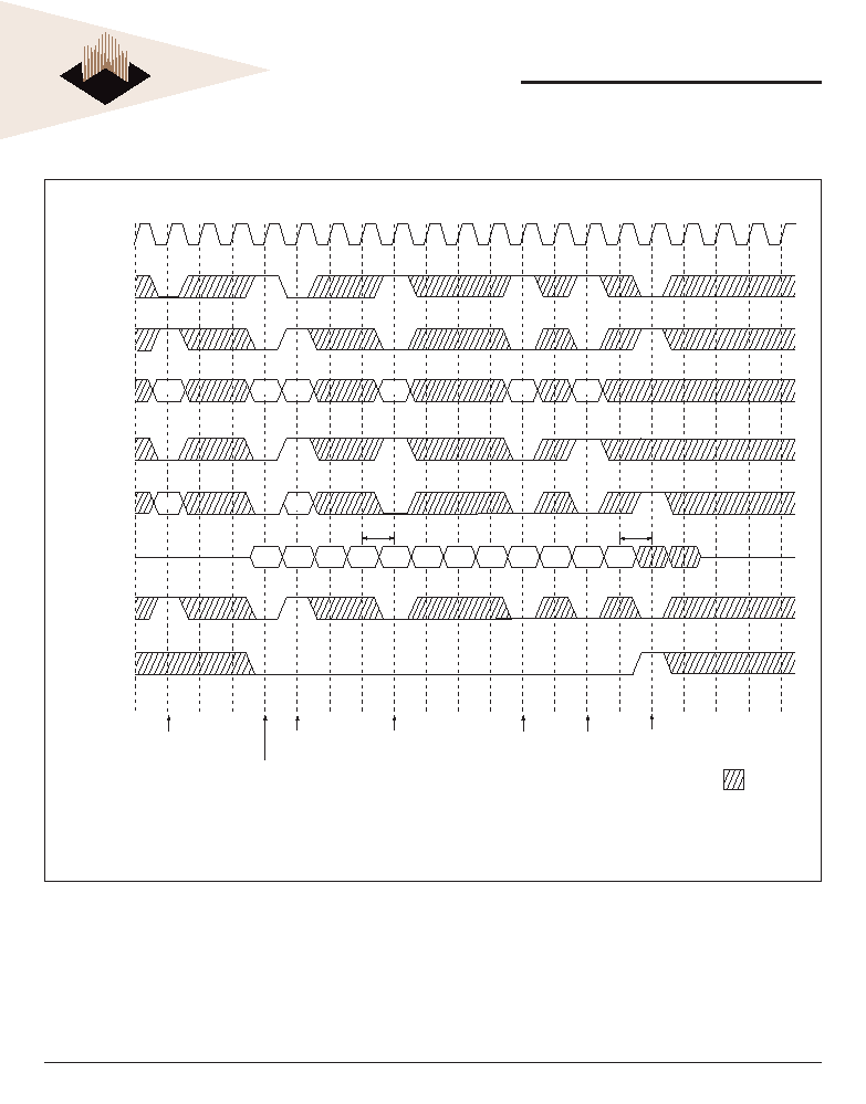
FIGURE 4 ≠ SDRAM SINGLE BIT READ-WRITE-READ CYCLE (SAME PAGE)
@CAS LATENCY = 3, BURST LENGTH = 1
GCK
VCRAS#
VCCAS#
VCADDR
VCBS
VCADDR9/AP
VCDATA
VCWE#
VCDQM#
Row Active
Read
Write
Read
Precharge
Row Active
DON' T CARE
0 1 2 3 4 5 6 7 8 9 10 11 12 13 14 15 16 17 18 19
t
CC
t
CH
t
CL
t
RCD
t
SS
t
SH
t
SS
t
SH
t
SS
t
SH
t
SS
t
SH
t
SS
t
SH
t
SS
t
SH
t
SS
t
SH
t
RCD
t
RAS
t
RP
t
CCD
t
RAC
t
SAC
t
SLZ
t
OH
Ra
Ra
Ca
BS
BS
BS
BS
BS
BS
Rb
Qc
Qa
Db
Cb
Cc
Rb
11
White Electronic Designs Corporation ∑ (602) 437-1520 ∑ www.wedc.com
White Electronic Designs
WED9LAPC2B16P8BC
November 2001
Rev. 1
White Electronic Designs Corp. reserves the right to change products or specifi cations without notice.
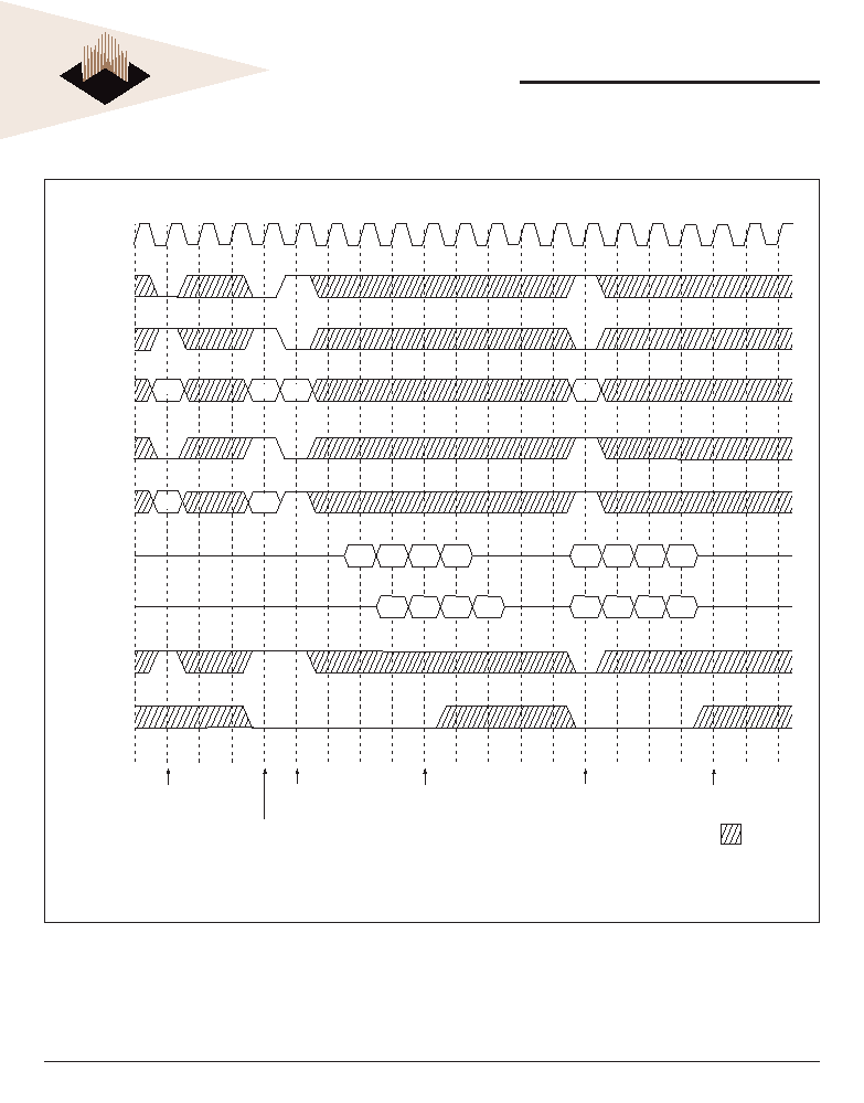
FIGURE 5 ≠ SDRAM READ & WRITE CYCLE AT SAME BANK @ BURST LENGTH = 4
0 1 2 3 4 5 6 7 8 9 10 11 12 13 14 15 16 17 18 19
GCK
VCRAS#
VCCAS#
VCADDR
VCBS
VCADDR9/AP
VCDATA
VCWE#
VCDQM#
CL = 2
CL = 3
Row Active
(A-Bank)
Row Active
(A-Bank)
Read
(A-Bank)
Write
(A-Bank)
Precharge
(A-Bank)
Precharge
(A-Bank)
DON'T CARE
t
RC
t
RCD
Note 1
Ra
Ca0
Cb0
Rb
Rb
Ra
t
RAC
t
RAC
Note 3
Note 3
t
SAC
t
SAC
t
OH
t
OH
t
SHZ
Note 4
t
SHZ
Note 4
t
RDL
t
RDL
Qa0
Qa1
Qa2
Qa3
Db0
Db1
Db2
Db3
Db0
Db1
Db2
Db3
Qa0
Qa1
Qa2
Qa3
Notes:
1. Minimum row cycle times are required to complete internal DRAM operation.
2. Row precharge can interrupt burst on any cycle. (CAS Latency - 1) number of valid output data is
available after Row precharge. Last valid output will be Hi-Z (t
SHZ
) after the clock.
3. Access time from Row active command. t
CC
*(t
RCD
+ CAS Latency - 1) + t
SAC
.
4. Output will be Hi-Z after the end of burst. (1, 2, 4, 8 & Full page bit burst)

12
White Electronic Designs Corporation ∑ (602) 437-1520 ∑ www.wedc.com
White Electronic Designs
WED9LAPC2B16P8BC
November 2001
Rev. 1
White Electronic Designs Corp. reserves the right to change products or specifi cations without notice.
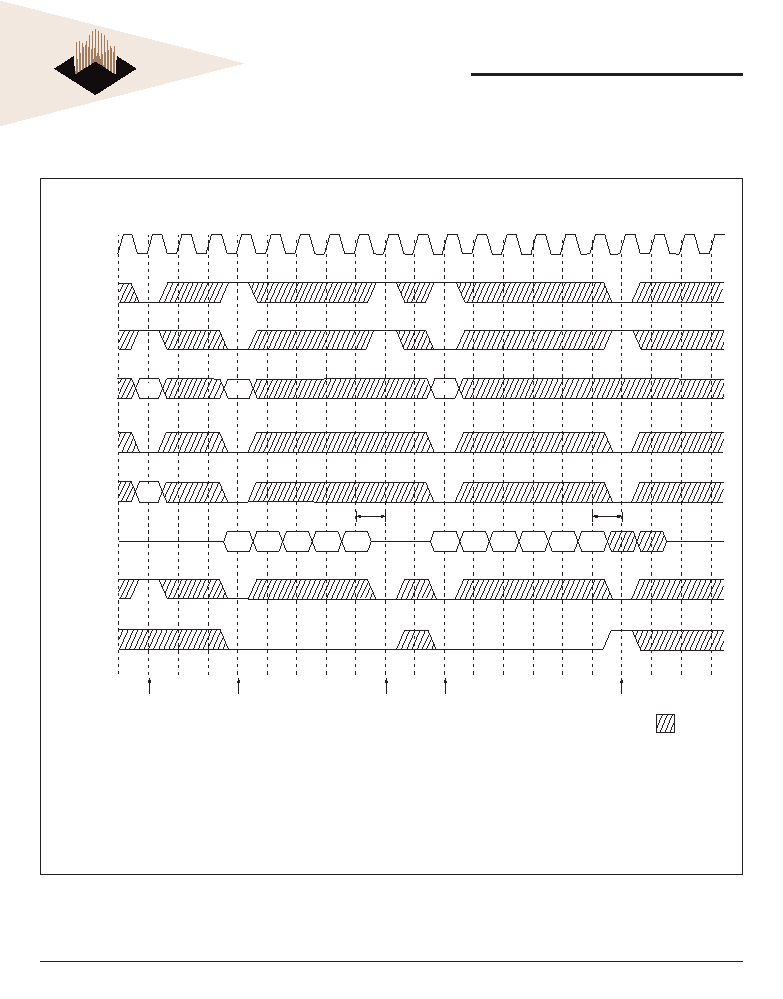
FIGURE 6 ≠ SDRAM PAGE READ & WRITE CYCLE AT SAME BANK @ BURST LENGTH = 4
0 1 2 3 4 5 6 7 8 9 10 11 12 13 14 15 16 17 18 19
GCK
VCRAS#
VCCAS#
VCADDR
VCBS
VCADDR9/AP
VCDATA
VCWE#
VCDQM#
CL = 2
CL = 3
Row Active
(A-Bank)
Read
(A-Bank)
Read
(A-Bank)
Write
(A-Bank)
Write
(A-Bank)
Precharge
(A-Bank)
DON'T CARE
t
RCD
Note 2
Ra
Ca0
Cb0
Cd0
Cc0
Ra
Note 3
t
CDL
Note 1
t
RDL
Qa0
Qa1
Qb0
Qb1
Dc0
Dc1
Dd0
Dd1
Dc0
Dc1
Dd0
Dd1
Qa0
Qa1
Qb2
Qb1
Qb2
Notes:
1. To write data before burst read ends. VCDQM# should be asserted three cycle prior to write command to avoid bus contention.
2. Row precharge will interrupt writing. Last data input, t
RDL
before Row precharge will be written.
3. VCDQM# should mask invalid input data on precharge command cycle when asserting precharge before end of burst. Input data
after Row precharge cycle will be masked internally.

13
White Electronic Designs Corporation ∑ (602) 437-1520 ∑ www.wedc.com
White Electronic Designs
WED9LAPC2B16P8BC
November 2001
Rev. 1
White Electronic Designs Corp. reserves the right to change products or specifi cations without notice.
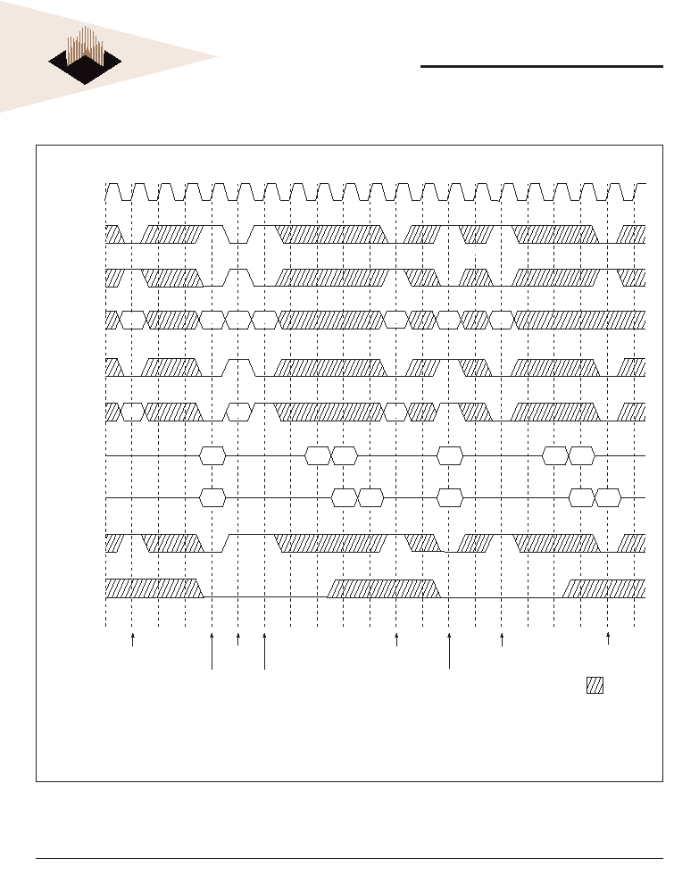
FIGURE 7 ≠ SDRAM PAGE READ CYCLE AT DIFFERENT BANK @ BURST LENGTH = 4
0 1 2 3 4 5 6 7 8 9 10 11 12 13 14 15 16 17 18 19
GCK
VCRAS#
VCCAS#
VCADDR
VCBS
VCADDR9/AP
VCDATA
VCWE#
VCDQM#
CL = 2
CL = 3
Row Active
(A-Bank)
Row Active
(B-Bank)
Read
(A-Bank)
Read
(A-Bank)
Read
(A-Bank)
Read
(B-Bank)
Read
(B-Bank)
Precharge
(A-Bank)
DON'T CARE
Note 1
RAa
CAa
CBb
CBd
CAc
CAe
RBb
RBb
RAa
QAa0
QAa1
QAa2
QAa3
QBb0
QBb1
QBb2
QBb3
QAc0
QAc1
QBd0
QBd1
QAe0
QAe1
QAa0
QAa1
QAa2
QAa3
QBb0
QBb1
QBb2
QBb3
QAc0
QAc1
QBd0
QBd1
QAe0
QAe1
Note:
1. To interrupt a burst read by Row precharge, both the read and the precharge banks must be the same.
14
White Electronic Designs Corporation ∑ (602) 437-1520 ∑ www.wedc.com
White Electronic Designs
WED9LAPC2B16P8BC
November 2001
Rev. 1
White Electronic Designs Corp. reserves the right to change products or specifi cations without notice.
FIGURE 8 ≠ SDRAM PAGE WRITE CYCLE AT DIFFERENT BANK @ BURST LENGTH = 4
0 1 2 3 4 5 6 7 8 9 10 11 12 13 14 15 16 17 18 19
GCK
VCRAS#
VCCAS#
VCADDR
VCBS
VCADDR9/AP
VCDATA
VCWE#
VCDQM#
Row Active
(A-Bank)
Row Active
(B-Bank)
Write
(A-Bank)
Write
(A-Bank)
Write
(B-Bank)
Write
(B-Bank)
Precharge
(Both Banks)
DON'T CARE
Note 2
RAa
CAa
RBb
CBb
CBd
CAc
RAa
RBb
Note 1
t
RDL
t
CDL
DBb0
DBb1
DBb2
DBb3
DAc0
DAc1
DBd0
DBd1
DAa0
DAa1
DAa2
DAa3
NOTES:
1. To interrupt burst write by Row precharge, VCDQM# should be asserted to mask invalid input data.
2. To interrupt a burst read by Row precharge, both the read and the precharge banks must be the same.

15
White Electronic Designs Corporation ∑ (602) 437-1520 ∑ www.wedc.com
White Electronic Designs
WED9LAPC2B16P8BC
November 2001
Rev. 1
White Electronic Designs Corp. reserves the right to change products or specifi cations without notice.
FIGURE 9 ≠ SDRAM READ & WRITE CYCLE AT DIFFERENT BANK @ BURST LENGTH = 4
Note:
1. t
CDL
should be met to complete write.
0 1 2 3 4 5 6 7 8 9 10 11 12 13 14 15 16 17 18 19
GCK
VCRAS#
VCCAS#
VCADDR
VCBS
VCADDR9/AP
VCDATA
VCWE#
VCDQM#
CL = 2
CL = 3
Row Active
(A-Bank)
Row Active
(B-Bank)
Row Active
(A-Bank)
Read
(A-Bank)
Read
(A-Bank)
Write
(B-Bank)
Precharge
(A-Bank)
DON'T CARE
RAa
CAa
RBb
RBb
RAc
RAc
CBb
CAc
RAa
Note 1
t
CDL
QAa0
QAa1
QAa2
QAa3
QAa0
QAa1
QAa2
QAa3
DBb0
DBb1
DBb2
DBb3
QAc0
QAc1
QAc0
QAc1
QAc2
DBb0
DBb1
DBb2
DBb3
16
White Electronic Designs Corporation ∑ (602) 437-1520 ∑ www.wedc.com
White Electronic Designs
WED9LAPC2B16P8BC
November 2001
Rev. 1
White Electronic Designs Corp. reserves the right to change products or specifi cations without notice.
FIGURE 10 ≠ SDRAM READ & WRITE CYCLE WITH AUTO PRECHARGE @BURST LENGTH = 4
0 1 2 3 4 5 6 7 8 9 10 11 12 13 14 15 16 17 18 19
GCK
VCRAS#
VCCAS#
VCADDR
VCBS
VCADDR9/AP
VCDATA
VCWE#
VCDQM#
CL = 2
CL = 3
Row Active
(A-Bank)
Row Active
(B-Bank)
Read with
Auto Precharge
(A-Bank)
Write with
Auto Precharge
(B-Bank)
Auto Precharge
Start Point
(A-Bank)
Auto Precharge
Start Point
(B-Bank)
DON'T CARE
Ra
Ca
Cb
Rb
Rb
Ra
Qa0
Qa1
Qa2
Qa3
Db0
Db1
Db2
Db3
Db0
Db1
Db2
Db3
Qa0
Qa1
Qa2
Qa3
Note:
1. t
CDL
should be controlled to meet minimum t
RAS
before internal precharge start.
(In the case of Burst Length = 1 & 2 and BRSW mode)

17
White Electronic Designs Corporation ∑ (602) 437-1520 ∑ www.wedc.com
White Electronic Designs
WED9LAPC2B16P8BC
November 2001
Rev. 1
White Electronic Designs Corp. reserves the right to change products or specifi cations without notice.
FIGURE 11 ≠ SDRAM READ INTERRUPTED BY PRECHARGE COMMAND & READ BURST STOP
@ BURST LENGTH = FULL PAGE
0 1 2 3 4 5 6 7 8 9 10 11 12 13 14 15 16 17 18 19
GCK
VCRAS#
VCCAS#
VCADDR
VCBS
VCADDR9/AP
VCDATA
VCWE#
VCDQM#
CL = 2
CL = 3
Row Active
(A-Bank)
Read
(A-Bank)
Read
(A-Bank)
Burst Stop
Precharge
(A-Bank)
DON'T CARE
RAa
CAa
CAb
RAa
Note 2
QAa0
QAa1
QAa2
QAa3
QAa4
QAb0
QAb1
QAb2
QAb3
QAb4
QAb5
QAb0
QAb1
QAb2
QAb3
QAb4
QAb5
QAa0
QAa1
QAa2
QAa3
QAa4
1
2
2
1
Notes:
1. At full page mode, burst is end at the end of burst. So auto precharge is possible.
2. About the valid VCDATAs after burst stop, it is the same as the case of VCRAS# interrupt. Both cases are illustrated in the above timing diagram. See the label 1, 2 on
each of them. But at burst write, burst stop and VCRAS# interrupt should be compared carefully. Refer to the timing diagram of "Full page write burst stop cycle."
3. Burst stop is valid at every burst length.
18
White Electronic Designs Corporation ∑ (602) 437-1520 ∑ www.wedc.com
White Electronic Designs
WED9LAPC2B16P8BC
November 2001
Rev. 1
White Electronic Designs Corp. reserves the right to change products or specifi cations without notice.
FIGURE 12 ≠ SDRAM WRITE INTERRUPTED BY PRECHARGE COMMAND & WRITE BURST STOP
@ BURST LENGTH = FULL PAGE
0 1 2 3 4 5 6 7 8 9 10 11 12 13 14 15 16 17 18 19
GCK
VCRAS#
VCCAS#
VCADDR
VCBS
VCADDR9/AP
VCDATA
VCWE#
VCDQM#
Row Active
(A-Bank)
Write
(A-Bank)
Write
(A-Bank)
Burst Stop
Precharge
(A-Bank)
DON'T CARE
RAa
CAa
CAb
RAa
t
RDL
Note 2
t
BDL
DAb0
DAb1
DAb2
DAb3
DAb4
DAb5
DAa0
DAa1
DAa2
DAa3
DAa4
Notes:
1. At full page mode, burst is end at the end of burst. So auto precharge is possible.
2. Data-in at the cycle of interrupted by precharge can not be written into the corresponding memory
cell. It is defi ned by AC parameter of t
RDL
.
VCDQM# at write interrupt by precharge command is needed to prevent invalid write.
VCDQM# should mask invalid input data on precharge command cycle when asserting precharge
before end of burst. Input data after Row precharge cycle will be masked internally.
3. Burst stop is valid at every burst length.
19
White Electronic Designs Corporation ∑ (602) 437-1520 ∑ www.wedc.com
White Electronic Designs
WED9LAPC2B16P8BC
November 2001
Rev. 1
White Electronic Designs Corp. reserves the right to change products or specifi cations without notice.
FIGURE 13 ≠ SDRAM BURST READ SINGLE BIT WRITE CYCLE @ BURST LENGTH = 2
0 1 2 3 4 5 6 7 8 9 10 11 12 13 14 15 16 17 18 19
GCK
VCRAS#
VCCAS#
VCADDR
VCBS
VCADDR9/AP
VCDATA
VCWE#
VCDQM#
CL = 2
CL = 3
Row Active
(A-Bank)
Row Active
(B-Bank)
Row Active
(A-Bank)
Write
(A-Bank)
Read
(A-Bank)
Write with
Auto Precharge
(B-Bank)
Read with
Auto Precharge
(A-Bank)
Precharge
(Both Banks)
DON'T CARE
Note 2
RAa
CAa
CBc
CAd
RAc
RAa
DAa0
RBb
CAb
DBc0
DBc0
RAc
QAd0
QAd1
QAd0
QAd1
DAa0
RBb
QAb0
QAb1
QAb0
QAb1
Notes:
1. BRSW modes enabled by setting A9 "High" at MRS (Mode Register Set).
At the BRSW Mode, the burst length at Write is fi xed to "1" regardless of programmed burst length.
2. When BRSW write command with auto precharge is executed, keep it in mind that t
RAS
should not be violated. Auto precharge is executed at the burst-end cycle, so in the
case of BRSW write command, the next cycle starts the precharge.

20
White Electronic Designs Corporation ∑ (602) 437-1520 ∑ www.wedc.com
White Electronic Designs
WED9LAPC2B16P8BC
November 2001
Rev. 1
White Electronic Designs Corp. reserves the right to change products or specifi cations without notice.
FIGURE 14 ≠ SDRAM MODE REGISTER SET CYCLE
0 1 2 3 4 5 6
GCK
VCRAS#
VCCAS#
VCADDR
VCDATA
VCWE#
VCDQM#
MRS
New
Command
DON'T CARE
Note 2
HI-Z
Note 1
Note 3
Key
Ra
*Both banks precharge should be completed before Mode Register Set cycle.
NOTES:
MODE REGISTER SET CYCLE
1. VCRAS#, VCCAS# & VCWE# activation at the same clock cycle with address key will set internal mode register.
2. Minimum 2 clock cycles should be met before new VCRAS# activation.
3. Please refer to Mode Register Set table.

21
White Electronic Designs Corporation ∑ (602) 437-1520 ∑ www.wedc.com
White Electronic Designs
WED9LAPC2B16P8BC
November 2001
Rev. 1
White Electronic Designs Corp. reserves the right to change products or specifi cations without notice.
PACKAGE DESCRIPTION: 153 LEAD BGA 14MM X 22MM
ORDERING INFORMATION
WED9LAPC2C16P8BC
Commercial Temperature:
0∫C to +70∫C
WED9LAPC2C16P8BI
Industrial Temperature:
-40∫C to +85∫C
Note: Ball attach pad for above BGA package is 480 microns in diameter. Pad is solder mask defi ned.