1
White Electronic Designs Corporation (508) 366-5151 www.whiteedc.com
White Electronic Designs
WED9LC6816V
August 2002 Rev 0
ECO #14663
256Kx32 SSRAM/4Mx32 SDRAM
External Memory Solution for Texas Instruments
TMS320C6000 DSP
FEATURES
n
Clock speeds:
SSRAM: 200, 166,150, and 133 MHz
SDRAMs: 125 and 100 MHz
n
DSP Memory Solution
Texas Instruments TMS320C6201
Texas Instruments TMS320C6701
n
Packaging:
153 pin BGA, JEDEC MO-163
n
3.3V Operating supply voltage
n
Direct control interface to both the SSRAM and
SDRAM ports on the C6x
n
Common address and databus
n
65% space savings vs. monolithic solution
n
Reduced system inductance and capacitance
DESCRIPTION
The WED9LC6816V is a 3.3V, 256K x 32 Synchronous
Pipeline SRAM and a 4Mx32 Synchronous DRAM array
constructed with one 256K x 32 SBSRAM and two 4Mx16
SDRAM die mounted on a multilayer laminate sub-
strate. The device is packaged in a 153 lead, 14mm by
22mm, BGA.
The WED9LC6816V provides a total memory solution
for the Texas Instruments TMS320C6201 and the
TMS320C6701 DSPs The Synchronous Pipeline SRAM
is available with clock speeds of 200, 166,150,v and
133 MHz, allowing the user to develop a fast external
memory for the SSRAM interface port .
The SDRAM is available in clock speeds of 125 and
100 MHz, allowing the user to develop a fast external
memory for the SDRAM interface port.
The WED9LC6816V is available in both commercial
and industrial temperature ranges.
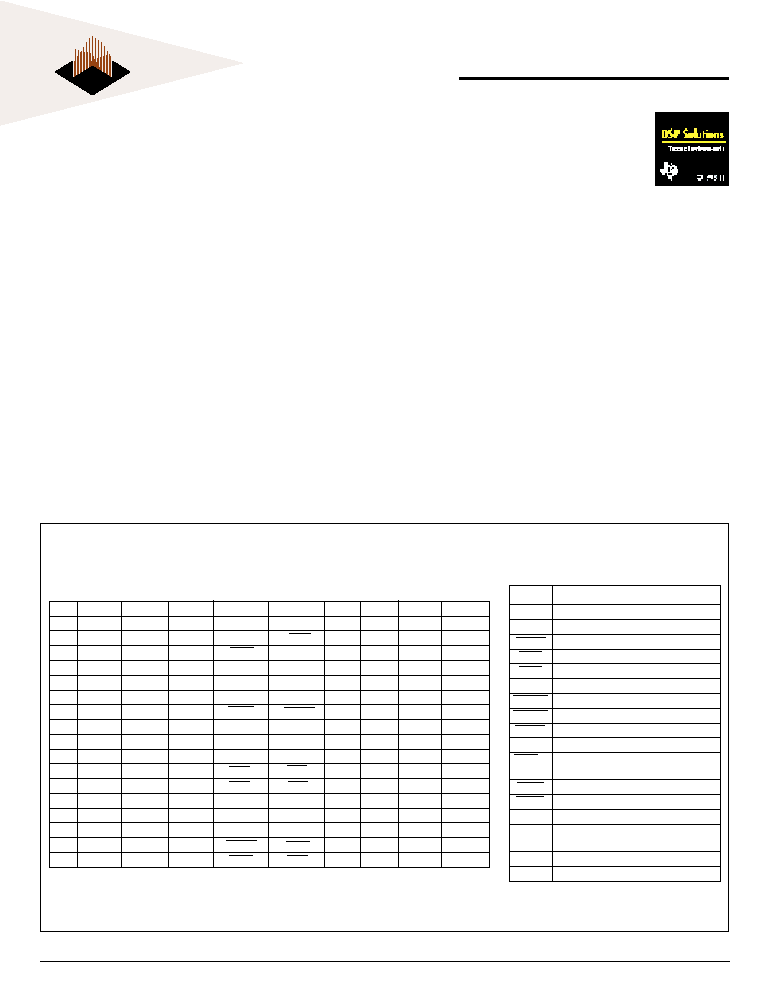
FIG. 1 PIN CONFIGURATION
1
2
3
4
5
6
7
8
9
A
DQ
19
DQ
23
V
CC
V
SS
V
SS
V
SS
V
CC
DQ
24
DQ
28
B
DQ
18
DQ
22
V
CC
V
SS
SDCE
V
SS
V
CC
DQ
25
DQ
29
C
V
CCQ
V
CCQ
V
CC
SDWE
SDA
10
NC
V
CC
V
CCQ
V
CCQ
D
DQ
17
DQ
21
V
CC
V
SS
V
SS
V
SS
V
CC
DQ
26
DQ
30
E
DQ
16
DQ
20
V
CC
V
SS
SDCLK
V
SS
V
CC
DQ
27
DQ
31
F
V
CCQ
V
CCQ
V
CC
V
SS
V
SS
V
SS
V
CC
V
CCQ
V
CCQ
G
NC
NC
NC
SDRAS
SDCAS
V
SS
A
2
A
4
A
5
H
NC
NC
A
8
V
SS
V
SS
NC
A
1
A
3
A
10
J
A
6
A
7
A
9
V
SS
V
SS
NC
A
0
A
11
A
12
K
A
17
NC/A
18
NC/A
19
V
SS
V
SS
NC
NC
A
13
A
14
L
NC
NC
NC
BWE
2
BWE
3
NC
NC
A
15
A
16
M
V
CCQ
V
CCQ
V
CC
BWE
0
BWE
3
NC
NC
A
15
A
16
N
DQ
12
DQ
11
V
CC
V
SS
V
SS
V
SS
V
CC
DQ
4
DQ
0
P
DQ
13
DQ
10
V
CC
V
SS
SSCLK
V
SS
V
CC
DQ
5
DQ
1
R
V
CCQ
V
CCQ
V
CC
V
SS
V
SS
V
SS
Vcc
V
CCQ
V
CCQ
T
DQ
14
DQ
9
V
CC
SSADC
SSWE
NC
V
CC
DQ
6
DQ
2
UDQ
15
DQ
8
V
CC
SSOE
SSCE
NC
V
CC
DQ
7
DQ
3
A
0-17
Address Bus
DQ
0-31
Data Bus
SSCLK
SSRAM Clock
SSADC
SSRAM Address Status Control
SSWE
SSRAM Write Enable
SSOE
SSRAM Output Enable
SDCLK
SDRAM Clock
SDRAS
SDRAM Row Address Strobe
SDCAS SDRAM Column Address Strobe
SDWE
SDRAM Write Enable
SDA
10
SDRAM Address
10/auto precharge
BWE
0-3
SSRAM Byte Write Enables
SDRAM SDQM 0-3
SSCE
Chip Enable SSRAM Device
SDCE
Chip Enable SDRAM Device
V
CC
Power Supply pins, 3.3V
V
CCQ
Data Bus Power Supply pins,
3.3V (2.5V future)
V
SS
Ground
NC
No Contact
T
OP
V
IEW
P
IN
D
ESCRIPTION
2
White Electronic Designs Corporation Westborough, MA (508) 366-5151
White Electronic Designs
WED9LC6816V
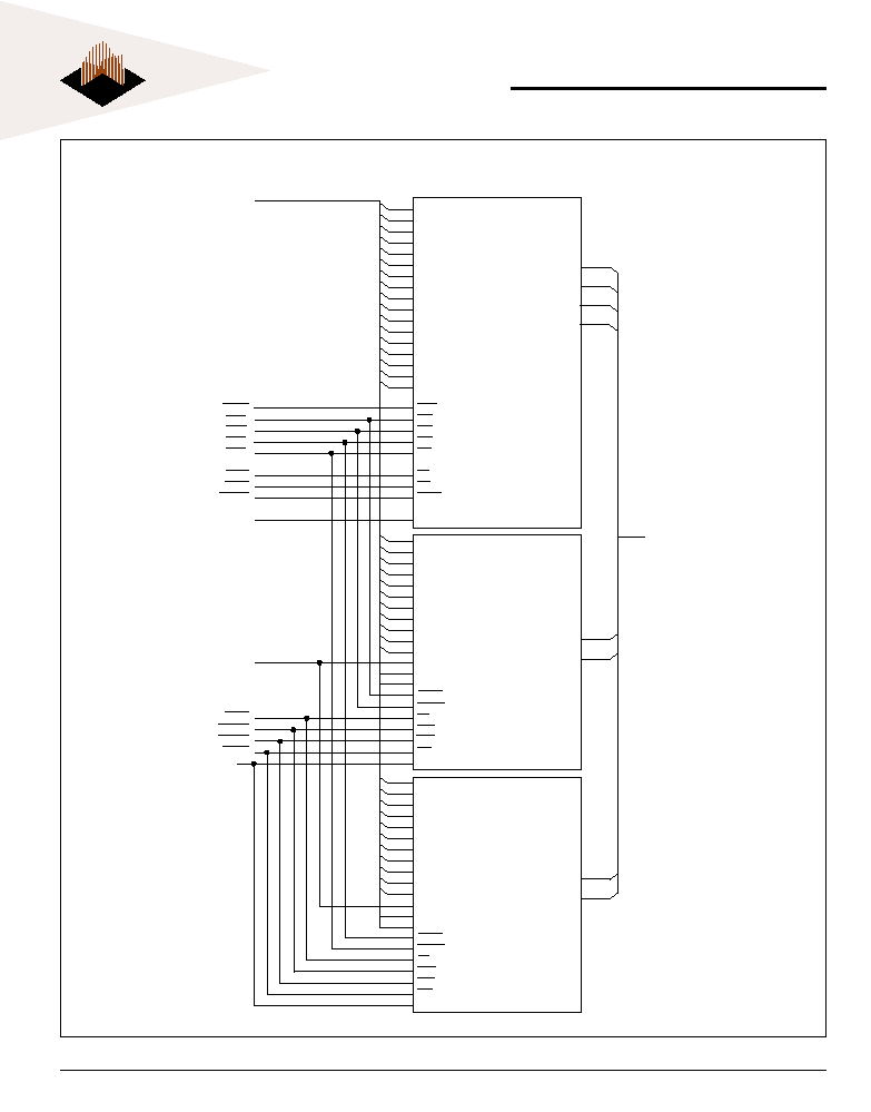
FIG. 2 BLOCK DIAGRAM
DQ
8-15
DQ
0-7
DQ
9-16
DQ
1-8
DQ
8-15
DQ
0-7
A
0-17
DQ
8-15
DQ
0-7
A
0
A
1
A
2
A
3
A
4
A
5
A
6
A
7
A
8
A
9
A
10
A
11
A
12
A
13
A
14
A
15
A
16
BWE
BW
1
BW
2
BW
3
BW
4
CE
2
OE
ADSC
CLK
DQ
0-31
A
0
A
1
DQ
24-31
DQ
16-23
DQ
25-32
DQ
17-24
A
0
A
1
A
2
A
3
A
4
A
5
A
6
A
7
A
8
A
9
A
11
A
10
/AP
BA
0
BA
1
LDQM
UDQM
CS
RAS
CAS
WE
CLK
A
0
A
1
A
2
A
3
A
4
A
5
A
6
A
7
A
8
A
9
A
11
A
10
/AP
BA
0
BA
1
LDQM
UDQM
CS
RAS
CAS
WE
CLK
A
12
A
13
A
12
A
13
DQ
8-15
DQ
0-7
DQ
24-31
DQ
16-23
SSWE
BWE
0
BWE
1
BWE
2
BWE
3
SSCE
SSOE
SSADC
SSCLK
SDA
10
SDCE
SDRAS
SDCAS
SDWE
SDCLK
3
White Electronic Designs Corporation (508) 366-5151 www.whiteedc.com
White Electronic Designs
WED9LC6816V
O
UTPUT
F
UNCTIONAL
D
ESCRIPTIONS
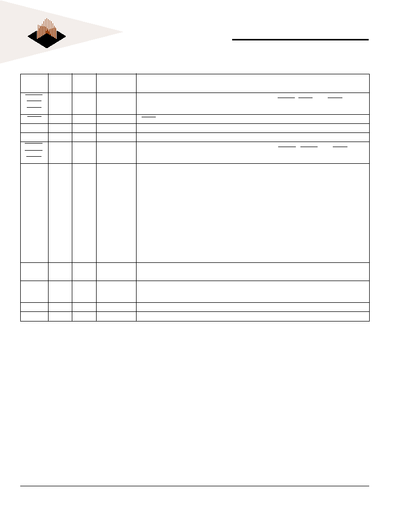
Symbol
Type
Signal
Polarity
Function
SSCLK
Input
Pulse
Positive Edge
The system clock input. All of the SSRAM inputs are sampled on the rising edge of the clock.
SSADS
When sampled at the positive rising edge of the clock, SSADS, SSOE, and SSWE define
SSOE
Input
Pulse
Active Low
SSWE
the operation to be executed by the SSRAM.
SSCE
Input
Pulse
Active Low
SSCE disable or enable SSRAM device operation.
SDCLK
Input
Pulse
Positive Edge
The system clock input. All of the SDRAM inputs are sampled on the rising edge of the clock.
SDCE
Input
Pulse
Active Low
SDCE disable or enable device operation by masking or enabling all inputs except SDCLK and BWE
0-3
.
SDRAS
When sampled at the positive rising edge of the clock, SDCAS, SDRAS, and SDWE define
SDCAS
Input
Pulse
Active Low
SDWE
the operation to be executed by the SDRAM.
Address bus for SSRAM and SDRAM
A
0
and A
1
are the burst address inputs for the SSRAM
During a Bank Active command cycle, A
0-11
, SDA
10
defines the row address (RA
0-10
)
when sampled at the rising clock edge.
During a Read or Write command cycle, A
0-7
defines the column address (CA
0-7
) when
A
0-17
,
Input
Level
sampled at the rising clock edge. In addition to the row address, SDA
10
is used to invoke
SDA10
Autoprecharge operation at the end of the Burst Read or Write Cycle. If SDA
10
is high,
autoprecharge is selected and A
12
and A
13
define the bank to be precharged. If SDA
10
is
low, autoprecharge is disabled.
During a Precharge command cycle, SDA
10
is used in conjunction with A
12
and A
13
to
control which bank(s) to precharge. If SDA
10
is high, all banks will be precharged regardless
of the state of A
12
and A
13
. If SDA
10
is low, then A
12
and A
13
are used to define which
bank to precharge.
DQ
0-31
Input
Level
Data Input/Output are multiplexed on the same pins.
Output
BWE
0-3
perform the byte write enable function for the SSRAM and DQM function for the
BWE
0-3
Input
Pulse
SDRAM. BWE
0
is associated with DQ
0-7
, BWE
1
with DQ
8-15
, BWE
2
with DQ
16-23
and BWE
3
with DQ
24-31
.
V
CC
, V
SS
Supply
Power and ground for the input buffers and the core logic.
V
CCQ
Supply
Data base power supply pins, 3.3V (2.5V future).
4
White Electronic Designs Corporation Westborough, MA (508) 366-5151
White Electronic Designs
WED9LC6816V
A
BSOLUTE
M
AXIMUM
R
ATINGS
Voltage on V
CC
Relative to V
SS
-0.5V to +4.6V
Vin (DQx)
-0.5V to Vcc +0.5V
Storage Temperature (BGA)
-55�C to +125�C
Junction Temperature
+150�C
Short Circuit Output Current
100 mA
*Stress greater than those listed under "Absolute Maximum Ratings"
may cause permanent damage to the device. This is a stress rating
only and functional operation of the device at these or any other
conditions greater than those indicated in operational sections of
this specifications is not implied. Exposure to absolute maximum
rating conditions for extended periods may affect reliability.
R
ECOMMENDED
DC O
PERATING
C
ONDITIONS
(V
CC
= 3.3V -5% / +10%
UNLESS
OTHERWISE
NOTED
; 0�C � T
A
� 70�C,
C
OMMERCIAL
; -40�C� T
A
� 85�C, I
NDUSTRIAL
)
Parameter
Symbol Min
Max
Units
Supply Voltage (1)
V
CC
3.135
3.6
V
Input High Voltage (1,2)
V
IH
2.0 V
CC
+0.3
V
Input Low Voltage (1,2)
V
IL
-0.3
0.8
V
Input Leakage Current
IL
I
-10
10
�A
0 � V
IN
� V
CC
Output Leakage (Output Disabled)
IL
O
-10
10
�A
0 � V
IN
� V
CC
SSRAM Output High (I
OH
= -4mA) (1)
V
OH
2.4
V
SSRAM Output Low (I
OL
= 8mA) (1)
V
OL
0.4
V
SDRAM Output High (I
OH
= -2mA)
V
OH
2.4
V
SDRAM Output Low (I
OL
= 2mA)
V
OL
0.4
V
NOTES:
1. All voltages referenced to V
SS
(GND).
2. Overshoot: V
IH
� +6.0V for t � t
KC
/2
Underershoot: V
IL
� -2.0V for t � t
KC
/2
DC E
LECTRICAL
C
HARACTERISTICS
(V
CC
= 3.3V -5% / +10%
UNLESS
OTHERWISE
NOTED
; 0�C � T
A
� 70�C, C
OMMERCIAL
; -40�C � T
A
� 85�C, I
NDUSTRIAL
)
Description
Conditions
Symbol Frequency
Typ
Max
Units
133MHz
500
625
Power Supply Current:
150MHz
500
650
Operating (1,2,3)
SSRAM Active / DRAM Auto Refresh
I
CC
1
166MHz
550
700
mA
200MHz
600
800
133MHz
325
425
Power Supply Current
150MHz
350
450
Operating (1,2,3)
SSRAM Active / DRAM Idle
I
CC
2
166MHz
400
495
mA
200MHz
450
585
Power Supply Current
83MHz
500
625
SSRAM Active / SSRAM Idle
I
CC
3
100MHz
500
650
mA
Operating (1,2,3)
125MHz
550
700
SSCE and SDCE � V
CC
-0.2V,
CMOS Standby
All other inputs at V
SS
+0.2 � V
IN
or
I
SB
1
20.0
40.0
mA
V
IN
� V
CC
-0.2V, Clk frequency = 0
SSCE and SDCE � V
IH
min
TTL Standby
All other inputs at V
IL
max � V
IN
or
I
SB
2
30.0
55.0
mA
V
IN
� V
CC
-0.2V, Clk frequency = 0
Auto Refresh
I
CC
5
250
300
mA
NOTES:
1. I
CC
(operating) is specified with no output current. I
CC
(operating) increases with faster cycle times and greater output loading.
2. "Device idle" means device is deselected (CE = V
IH
) Clock is running at max frequency and Addresses are switching each cycle.
3. Typical values are measured at 3.3V, 25�C. I
CC
(operating) is specified at specified frequency.
BGA C
APACITANCE
Description
Conditions
Symbol
Typ
Max
Units
Address Input Capacitance (1)
T
A
= 25�C; f = 1MHz
C
I
5
8
pF
Input/Output Capacitance (DQ) (1)
T
A
= 25�C; f = 1MHz
C
O
8
10
pF
Control Input Capacitance (1)
T
A
= 25�C; f = 1MHz
C
A
5
8
pF
Clock Input Capacitance (1)
T
A
= 25�C; f = 1MHz
C
CK
4
6
pF
NOTE:
1. This parameter is sampled.

5
White Electronic Designs Corporation (508) 366-5151 www.whiteedc.com
White Electronic Designs
WED9LC6816V
SSRAM AC C
HARACTERISTICS
(V
CC
= 3.3V -5% / +10%
UNLESS
OTHERWISE
NOTED
; 0�C � T
A
� 70�C, C
OMMERCIAL
; -40�C � T
A
� 85�C, I
NDUSTRIAL
)
Symbol 200MHz 166MHz 150MHz 133MHz
Parameter
Min
Max
Min
Max
Min
Max
Min
Max
Units
Clock Cycle Time
t
KHKH
5
6
7
8
ns
Clock HIGH Time
t
KLKH
1.6
2.4
2.6
2.8
ns
Clock LOW Time
t
KHKL
1.6
2.4
2.6
2.8
ns
Clock to output valid
t
KHQV
2.5
3.5
3.8
4.0
ns
Clock to output invalid
t
KHQX
1.5
1.5
1.5
1.5
ns
Clock to output on Low-Z
t
KQLZ
0
0
0
0
ns
Clock to output in High-Z
t
KQHZ
1.5
3
1.5
3.5
1.5
3.8
1.5
4.0
ns
Output Enable to output valid
t
OELQV
2.5
3.5
3.8
4.0
ns
Output Enable to output in Low-Z
t
OELZ
0
0
0
0
ns
Output Enable to output in High-Z
t
OEHZ
3.0
3.5
3.5
3.8
ns
Address, Control, Data-in Setup Time to Clock
t
S
1.5
1.5
1.5
1.5
ns
Address, Control, Data-in Hold Time to Clock
t
H
0.5
0.5
0.5
0.5
ns
6
White Electronic Designs Corporation Westborough, MA (508) 366-5151
White Electronic Designs
WED9LC6816V
SSRAM O
PERATION
T
RUTH
T
ABLE
Operation
Address Used
SSCE
SSADS
SSWE
SSOE
DQ
Deselected Cycle, Power Down
None
H
L
X
X
High-Z
WRITE Cycle, Begin Burst
External
L
L
L
X
D
READ Cycle, Begin Burst
External
L
L
H
L
Q
READ Cycle, Begin Burst
External
L
L
H
H
High-Z
READ Cycle, Suspend Burst
Current
X
H
H
L
Q
READ Cycle, Suspend Burst
Current
X
H
H
H
High-Z
READ Cycle, Suspend Burst
Current
H
H
H
L
Q
READ Cycle, Suspend Burst
Current
H
H
H
H
High-Z
WRITE Cycle, Suspend Burst
Current
X
H
L
X
D
WRITE Cycle, Suspend Burst
Current
H
H
L
X
D
NOTE:
1. X means dont care, H means logic HIGH. L means logic LOW.
2. All inputs except SSOE must meet setup and hold times around the rising edge (LOW to HIGH) of SSCLK.
3. Suspending burst generates wait cycle
4. For a write operation following a read operation, SSOE must be HIGH before the input data required setup time plus High-Z time for SSOE and
staying HIGH through out the input data hold time.
5. This device contains circuitry that will ensure the outputs will be in High-Z during power-up.
SSRAM P
ARTIAL
T
RUTH
T
ABLE
Function
SSWE BWE
0
BWE
1
BWE
2
BWE
3
READ
H
X
X
X
X
WRITE one Byte (DQ
0-7
)
L
L
H
H
H
WRITE all Bytes
L
L
L
L
L
7
White Electronic Designs Corporation (508) 366-5151 www.whiteedc.com
White Electronic Designs
WED9LC6816V
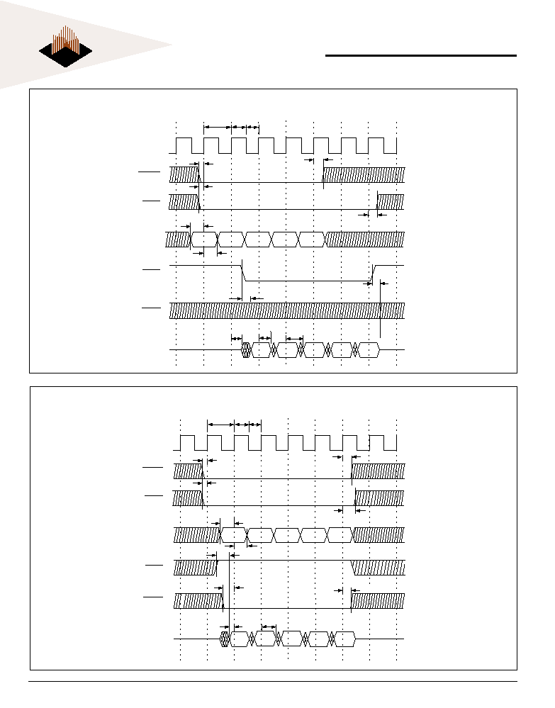
FIG. 3 SSRAM READ TIMING
SSCLK
SSWE
t
KHKL
t
KLKH
t
KHKH
SSCE
SSADS
t
S
t
S
t
S
t
H
t
H
DQ
t
KHQX
t
KQLZ
Q(A1)
Q(A2)
Q(A3)
Q(A4)
t
KHQV
Q(A5)
A5
ADDR
t
H
A1
A2
A3
A4
SSOE
t
OELQV
t
OEHZ
FIG. 4 SSRAM WRITE TIMING
t
KHK L
t
KLKH
t
KHK H
t
KHGWX
t
Must be HIGH
t
H
t
S
D(A1)
D(A2)
D(A3)
D(A4)
D(A5)
t
S
t
H
t
H
t
H
t
S
t
H
t
OEHZ
A1
A2
A3
A4
A5
S
H
SSCLK
SSWE
SSCE
SSADS
DQ
ADDR
SSOE

8
White Electronic Designs Corporation Westborough, MA (508) 366-5151
White Electronic Designs
WED9LC6816V
SDRAM AC C
HARACTERISTICS
(V
CC
= 3.3V -5% / +10%
UNLESS
OTHERWISE
NOTED
; 0�C�T
A
�70�C, C
OMMERCIAL
; -40�C�T
A
�85�C, I
NDUSTRIAL
)
Symbol 125MHz 100MHz 83MHz
Parameter
Min
Max
Min
Max
Min
Max
Units
Clock Cycle Time (1)
CL = 3
t
CC
8
1000
10
1000
12
1000
ns
CL = 2
t
CC
10
1000
12
1000
15
1000
Clock to valid Output delay (1,2)
t
SAC
6
7
8
ns
Output Data Hold Time (2)
t
OH
3
3
3
ns
Clock HIGH Pulse Width (3)
t
CH
3
3
3
ns
Clock LOW Pulse Width (3)
t
CL
3
3
3
ns
Input Setup Time (3)
t
S S
2
2
2
ns
Input Hold Time (3)
t
SH
1
1
1
ns
CLK to Output Low-Z (2)
t
SLZ
2
2
2
ns
CLK to Output High-Z
t
SHZ
7
7
8
ns
Row Active to Row Active Delay (4)
t
RRD
20
20
24
ns
RAS\ to CAS\ Delay (4)
t
RCD
20
20
24
ns
Row Precharge Time (4)
t
RP
20
20
24
ns
Row Active Time (4)
t
RAS
50
10,000
50
10,000
60
10,000
ns
Row Cycle Time - Operation (4)
t
RC
70
80
90
ns
Row Cycle Time - Auto Refresh (4,8)
t
RFC
70
80
90
ns
Last Data in to New Column Address Delay (5)
t
CDL
1
1
1
CLK
Last Data in to Row Precharge (5)
t
RDL
1
1
1
CLK
Last Data in to Burst Stop (5)
t
BDL
1
1
1
CLK
Column Address to Column Address Delay (6)
t
CCD
1.5
1.5
1.5
CLK
Number of Valid Output Data (7)
2
2
2
1
2
1
ea
NOTES:
1. Parameters depend on programmed CAS latency.
2. If clock rise time is longer than 1ns (t
rise
/2 -0.5)ns should be added to the parameter.
3. Assumed input rise and fall time = 1ns. If t
rise
of t
fall
are longer than 1ns. [(t
rise
= t
fall
)/2] - 1ns should be added to the parameter.
4. The minimum number of clock cycles required is detemined by dividing the minimum time required by the clock cycle time and then rounding up
to the next higher integer.
5. Minimum delay is required to complete write.
6. All devices allow every cycle column address changes.
7. In case of row precharge interrupt, auto precharge and read burst stop.
8. A new command may be given t
RFC
after self-refresh exit.
9
White Electronic Designs Corporation (508) 366-5151 www.whiteedc.com
White Electronic Designs
WED9LC6816V
Frequency
CAS
t
RC
t
RAS
t
RP
t
RRD
t
RCD
t
CCD
t
CDL
t
RDL
Latency
70ns
50ns
20ns
20ns
20ns
10ns
10ns
10ns
125MHz (8.0ns)
3
9
6
3
2
3
1
1
1
100MHz (10.0ns)
3
7
5
2
2
2
1
1
1
83MHz (12.0ns)
2
6
4
2
2
2
1
1
1
C
LOCK
F
REQUENCY
AND
L
ATENCY
P
ARAMETERS
- 125MH
Z
SDRAM
(U
NIT
=
NUMBER
OF
CLOCK
)
Frequency
CAS
t
RC
t
RAS
t
RP
t
RRD
t
RCD
t
CCD
t
CDL
t
RDL
Latency
70ns
50ns
20ns
20ns
20ns
10ns
10ns
10ns
100MHz (12.0ns)
3
7
5
2
2
2
1
1
1
83MHz (12.0ns)
2
6
5
2
2
2
1
1
1
C
LOCK
F
REQUENCY
AND
L
ATENCY
P
ARAMETERS
- 100MH
Z
SDRAM
(U
NIT
=
NUMBER
OF
CLOCK
)
-10
-12
Parameter
Symbol
Min
Max
Min
Max
Units
Refresh Period (1,2)
t
REF
64
64
ms
R
EFRESH
C
YCLE
P
ARAMETERS
NOTES:
1. 4096 cycles
2. Any time that the Refresh Period has been exceeded, a minimum of two Auto (CBR) Refresh commands must be given to "wake-up" the device.
SDRAM C
OMMAND
T
RUTH
T
ABLE
Function
SDCE
SDRAS
SDCAS
SDWE
BWE
A
12
, A
13
SDA
10
Notes
A
11-0
Mode Register Set
L
L
L
L
X OP CODE
Auto Refresh (CBR)
L
L
L
H
X
X
X
Precharge
Single Bank
L
L
H
L
X
BA
L
2
Precharge all Banks
L
L
H
L
X
X
H
Bank Activate
L
L
H
H
X
BA
Row Address
2
Write
L
H
L
L
X
BA
L
2
Write with Auto Precharge
L
H
L
L
X
BA
H
2
Read
L
H
L
L
X
BA
L
2
Read with Auto Precharge
L
H
L
H
X
BA
H
2
Burst Termination
L
H
H
L
X
X
X
3
No Operation
L
H
H
H
X
X
X
Device Deselect
H
X
X
X
X
X
X
Data Write/Output Disable
X
X
X
X
L
X
X
4
Data Mask/Output Disable
X
X
X
X
H
X
X
4
NOTES:
1. All of the SDRAM operations are defined by states of SDCE\, SDWE\, SDRAS\, SDCAS\, and BWE
0-3
at the positive rising edge of the clock.
2. Bank Select (BA), A
12
(BA
0
) and A
13
(BA
1
) select between different banks.
3. During a Burst Write cycle there is a zero clock delay, for a Burst Read cycle the delay is equal to the CAS latency.
4. The BWE has two functions for the data DQ Read and Write operations. During a Read cycle, when BWE goes high at a clock timing the data
outputs are disabled and become high impedance after a two clock delay. BWE also provides a data mask function for Write cycles. When it
activates, the Write operation at the clock is prohibited (zero clock latency).
10
White Electronic Designs Corporation Westborough, MA (508) 366-5151
White Electronic Designs
WED9LC6816V
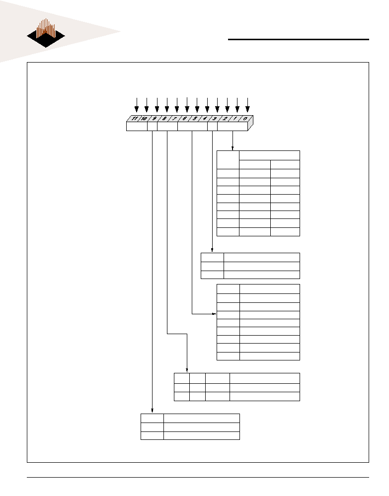
MODE REGISTER SET TABLE
M3 = 0
1
2
4
8
Reserved
Reserved
Reserved
Full Page
M3 = 1
1
2
4
8
Reserved
Reserved
Reserved
Reserved
Operating Mode
Standard Operation
All other states reserved
0
-
0
-
Defined
-
0
1
Burst Type
Sequential
Interleaved
CAS Latency
Reserved
Reserved
2
3
Reserved
Reserved
Reserved
Reserved
Burst Length
M0
0
1
0
1
0
1
0
1
Burst Length
CAS Latency
BT
A
9
A
7
A
6
A
5
A
4
A
3
A
8
A
2
A
1
A
0
Mode Register (Mx)
Address Bus
M1
0
0
1
1
0
0
1
1
M2
0
0
0
0
1
1
1
1
M3
M4
0
1
0
1
0
1
0
1
M5
0
0
1
1
0
0
1
1
M6
0
0
0
0
1
1
1
1
M6-M0
M8
M7
Op Mode
A
10
A
11
Reserved* WB
0
1
Write Burst Mode
Programmed Burst Length
Single Location Access
M9
*Should program
M11, M10 = "0, 0"
to ensure compatibility
with future devices.
11
White Electronic Designs Corporation (508) 366-5151 www.whiteedc.com
White Electronic Designs
WED9LC6816V
Command
Current State
Action
Notes
SDCE SDRAS SDCAS SDWE
A
12
& A
13
A
11
-A
0
Description
(BA)
L
L
L
L OP Code
Mode Register Set
Set the Mode Register
1
L
L
L
H
X
X
Auto or Self Refresh
Start Auto
1
L
L
H
L
X
X
Precharge
No Operation
L
L
H
H
BA
Row Address
Bank Activate
Activate the specified bank and row
Idle
L
H
L
L
BA
Column
Write w/o Precharge
ILLEGAL
2
L
H
L
H
BA
Column
Read w/o Precharge
ILLEGAL
1
L
H
H
L
X
X
Burst Termination
No Operation
1
L
H
H
H
X
X
No Operation
No Operation
H
X
X
X
X
X
Device Deselect
No Operation
L
L
L
L OP Code
Mode Register Set
ILLEGAL
L
L
L
H
X
X
Auto or Self Refresh
ILLEGAL
L
L
H
L
X
X
Precharge
Precharge
3
L
L
H
H
BA
Row Address
Bank Activate
ILLEGAL
1
Row Active
L
H
L
L
BA
Column
Write
Start Write; Determine if Auto Precharge
4,5
L
H
L
H
BA
Column
Read
Start Read; Determine if Auto Precharge
4,5
L
H
H
L
X
X
Burst Termination
No Operation
L
H
H
H
X
X
No Operation
No Operation
H
X
X
X
X
X
Device Deselect
No Operation
L
L
L
L OP Code
Mode Register Set
ILLEGAL
L
L
L
H
X
X
Auto or Self Refresh
ILLEGAL
L
L
H
L
X
X
Precharge
Terminate Burst; Start the Precharge
L
L
H
H
BA
Row Address
Bank Activate
ILLEGAL
2
Read
L
H
L
L
BA
Column
Write
Terminate Burst; Start the Write cycle
5,6
L
H
L
H
BA
Column
Read
Terminate Burst; Start a new Read cycle
5,6
L
H
H
L
X
X
Burst Termination
Terminate the Burst
L
H
H
H
X
X
No Operation
Continue the Burst
H
X
X
X
X
X
Device Deselect
Continue the Burst
L
L
L
L OP Code
Mode Register Set
ILLEGAL
L
L
L
H
X
X
Auto or Self Refresh
ILLEGAL
L
L
H
L
X
X
Precharge
Terminate Burst; Start the Precharge
L
L
H
H
BA
Row Address
Bank Activate
ILLEGAL
2
Write
L
H
L
L
BA
Column
Write
Terminate Burst; Start a new Write cycle
5,6
L
H
L
H
BA
Column
Read
Terminate Burst; Start the Read cycle
5,6
L
H
H
L
X
X
Burst Termination
Terminate the Burst
L
H
H
H
X
X
No Operation
Continue the Burst
H
X
X
X
X
X
Device Deselect
Continue the Burst
L
L
L
L OP Code
Mode Register Set
ILLEGAL
L
L
L
H
X
X
Auto or Self Refresh
ILLEGAL
L
L
H
L
X
X
Precharge
ILLEGAL
2
Read with
L
L
H
H
BA
Row Address
Bank Activate
ILLEGAL
2
Auto Precharge
L
H
L
L
BA
Column
Write
ILLEGAL
L
H
L
H
BA
Colum n
Read
ILLEGAL
L
H
H
L
X
X
Burst Termination
ILLEGAL
L
H
H
H
X
X
No Operation
Continue the Burst
H
X
X
X
X
X
Device Deselect
Continue the Burst
SDRAM C
URRENT
S
TATE
T
RUTH
T
ABLE
12
White Electronic Designs Corporation Westborough, MA (508) 366-5151
White Electronic Designs
WED9LC6816V
SDRAM C
URRENT
S
TATE
T
RUTH
T
ABLE
(
CONT
.)
Command
Current State
Action
Notes
SDCE SDRAS SDCAS SDWE
A
12
& A
13
A
11
-A
0
Description
(BA)
L
L
L
L OP Code
Mode Register Set
ILLEGAL
L
L
L
H
X
X
Auto or Self Refresh
ILLEGAL
L
L
H
L
X
X
Precharge
ILLEGAL
2
Write with
L
L
H
H
BA
Row Address
Bank Activate
ILLEGAL
2
Auto Precharge
L
H
L
L
BA
Column
Write
ILLEGAL
L
H
L
H
BA
Colum n
Read
ILLEGAL
L
H
H
L
X
X
Burst Termination
ILLEGAL
L
H
H
H
X
X
No Operation
Continue the Burst
H
X
X
X
X
X
Device Deselect
Continue the Burst
L
L
L
L OP Code
Mode Register Set
ILLEGAL
L
L
L
H
X
X
Auto or Self Refresh
ILLEGAL
L
L
H
L
X
X
Precharge
No Operation; Bank(s) idle after t
RP
L
L
H
H
BA
Row Address
Bank Activate
ILLEGAL
2
Precharging
L
H
L
L
BA
Column
Write w/o Precharge
ILLEGAL
2
L
H
L
H
BA
Column
Read w/o Precharge
ILLEGAL
20
L
H
H
L
X
X
Burst Termination
No Operation; Bank(s) idle after t
RP
L
H
H
H
X
X
No Operation
No Operation; Bank(s) idle after t
RP
H
X
X
X
X
X
Device Deselect
No Operation; Bank(s) idle after t
RP
L
L
L
L OP Code
Mode Register Set
ILLEGAL
L
L
L
H
X
X
Auto or Self Refresh
ILLEGAL
L
L
H
L
X
X
Precharge
ILLEGAL
2
L
L
H
H
BA
Row Address
Bank Activate
ILLEGAL
2
Row Activating
L
H
L
L
BA
Column
Write
ILLEGAL
2
L
H
L
H
BA
Colum n
Read
ILLEGAL
2
L
H
H
L
X
X
Burst Termination
No Operation; Row active after t
RCD
L
H
H
H
X
X
No Operation
No Operation; Row active after t
RCD
H
X
X
X
X
X
Device Deselect
No Operation; Row active after t
RCD
L
L
L
L OP Code
Mode Register Set
ILLEGAL
L
L
L
H
X
X
Auto orSelf Refresh
ILLEGAL
L
L
H
L
X
X
Precharge
ILLEGAL
2
L
L
H
H
BA
Row Address
Bank Activate
ILLEGAL
2
Write Recovering
L
H
L
L
BA
Column
Write
Start Write; Determine if Auto Precharge
6
L
H
L
H
BA
Column
Read
Start Read; Determine if Auto Precharge
6
L
H
H
L
X
X
Burst Termination
No Operation; Row active after t
DPL
L
H
H
H
X
X
No Operation
No Operation; Row active after t
DPL
H
X
X
X
X
X
Device Deselect
No Operation; Row active after t
DPL
L
L
L
L OP Code
Mode Register Set
ILLEGAL
L
L
L
H
X
X
Auto orSelf Refresh
ILLEGAL
L
L
H
L
X
X
Precharge
ILLEGAL
2
Write Recovering
L
L
H
H
BA
Row Address
Bank Activate
ILLEGAL
2
with Auto
L
H
L
L
BA
Column
Write
ILLEGAL
2,6
Precharge
L
H
L
H
BA
Column
Read
ILLEGAL
2,6
L
H
H
L
X
X
Burst Termination
No Operation; Precharge after t
DPL
L
H
H
H
X
X
No Operation
No Operation; Precharge after t
DPL
H
X
X
X
X
X
Device Deselect
No Operation; Precharge after t
DPL
13
White Electronic Designs Corporation (508) 366-5151 www.whiteedc.com
White Electronic Designs
WED9LC6816V
SDRAM C
URRENT
S
TATE
T
RUTH
T
ABLE
(
CONT
.)
Command
Current State
Action
Notes
SDCE SDRAS SDCAS SDWE
A
12
& A
13
A
11
-A
0
Description
(BA)
L
L
L
L OP Code
Mode Register Set
ILLEGAL
L
L
L
H
X
X
Auto or Self Refresh
ILLEGAL
L
L
H
L
X
X
Precharge
ILLEGAL
L
L
H
H
BA
Row Address
Bank Activate
ILLEGAL
Refreshing
L
H
L
L
BA
Column
Write
ILLEGAL
L
H
L
H
BA
Colum n
Read
ILLEGAL
L
H
H
L
X
X
Burst Termination
No Operation; Idle after t
RC
L
H
H
H
X
X
No Operation
No Operation; Idle after t
RC
H
X
X
X
X
X
Device Deselect
No Operation; Idle after t
RC
L
L
L
L OP Code
Mode Register Set
ILLEGAL
L
L
L
H
X
X
Auto or Self Refresh
ILLEGAL
L
L
H
L
X
X
Precharge
ILLEGAL
Mode Register
L
L
H
H
BA
Row Address
Bank Activate
ILLEGAL
Accessing
L
H
L
L
BA
Column
Write
ILLEGAL
L
H
L
H
BA
Colum n
Read
ILLEGAL
L
H
H
L
X
X
Burst Termination
ILLEGAL
L
H
H
H
X
X
No Operation
No Operation; Idle after two clock cycles
H
X
X
X
X
X
Device Deselect
No Operation; Idle after two clock cycles
NOTES:
1. Both Banks must be idle otherwise it is an illegal action.
2. The Current State refers only refers to one of the banks, if BA selects this bank then the action is illegal. If BA selects the bank not being
referenced by the Current State then the action may be legal depending on the state of that bank.
3. The minimum and maximum Active time (t
RAS
) must be satisfied.
4. The RAS to CAS Delay (t
RCD
) must occur before the command is given.
5. Address SDA
10
is used to determine if the Auto Precharge function is activated.
6. The command must satisfy any bus contention, bus turn around, and/or write recovery requirements.
The command is illegal if the minimum bank to bank delay time (t
RRD
) is not satisfied.
14
White Electronic Designs Corporation Westborough, MA (508) 366-5151
White Electronic Designs
WED9LC6816V
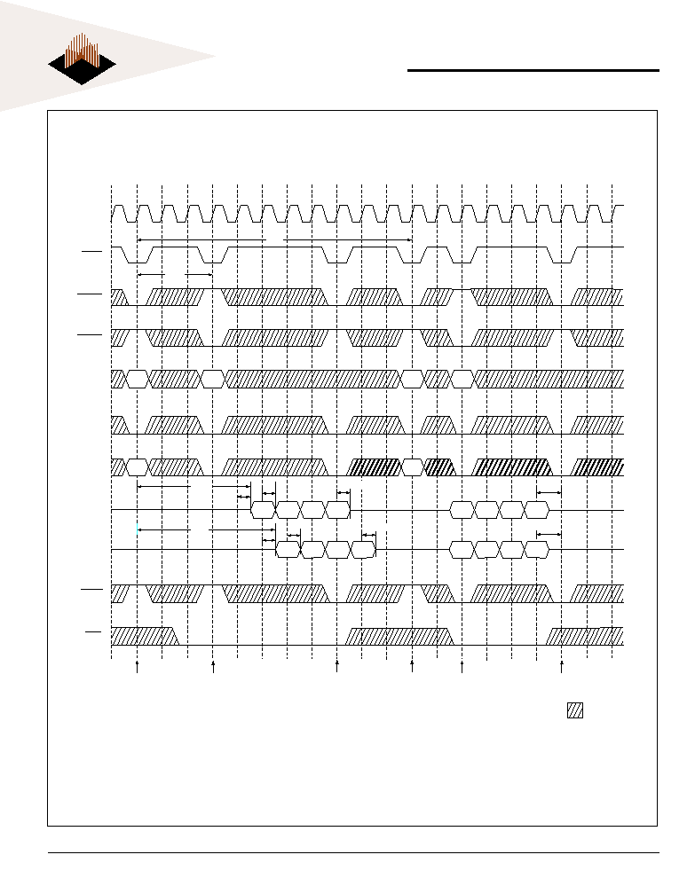
FIG. 5 SDRAM SINGLE BIT READ-WRITE-READ CYCLE (SAME PAGE) @
CAS LATENCY = 3, BURST LENGTH = 1
0
1
2
3
4
5
6
7 8 9 10 11 12 13 14 15 16 17 18 19
SDCLK
SDCE
SDRAS
SDCAS
ADDR
BA
0, 1
[A
12
,A
13
]
SDA
10
DQ
SDWE
BWE
t
CC
t
CH
t
CL
t
RCD
t
RAS
t
SS
t
SH
t
RCD
t
SS
t
SH
t
SS
t
SH
t
SS
t
SH
t
SS
t
SH
t
CCD
t
RP
t
RAC
t
SAC
t
SLZ
t
OH
t
SS
t
SS
t
SS
t
SH
t
SH
t
SH
Ra
Ca
Cb
Cc
Rb
BS
BS
BS
BS
BS
BS
Ra
Rb
Qa
Db
Qc
Row Active
Read
Write
Read
Precharge
Row Active
DON'T CARE

15
White Electronic Designs Corporation (508) 366-5151 www.whiteedc.com
White Electronic Designs
WED9LC6816V
FIG. 6 SDRAM POWER UP SEQUENCE
0
1
2
3
4
5
6
7 8 9 10 11 12 13 14 15 16 17 18 19
SDCLK
SDCE
SDRAS
SDCAS
ADDR
BA
0,1
[A
12
,A
13
]
SDA
10
DQ
SDWE
BWE
t
RP
HIGH-Z
Precharge
(All Banks)
Auto Refresh
Auto Refresh
Mode Register Set
DON'T CARE
Key
RAa
High level is necessary
RAa
t
RFC
t
RFC
Row Active
(A-Bank)
16
White Electronic Designs Corporation Westborough, MA (508) 366-5151
White Electronic Designs
WED9LC6816V
FIG. 7 SDRAM READ & WRITE CYCLE AT SAME BANK @
BURST LENGTH = 4
0
1
2
3
4
5
6
7 8 9 10 11 12 13 14 15 16 17 18 19
SDCLK
SDCE
SDRAS
SDWE
ADDR
Ra
Ca0
Cb0
CL=2
CL=3
t
RAC
Note 3
t
RAC
Note 3
t
SAC
t
SAC
t
SHZ
Note 4
t
SHZ
Note 4
Qa0
Qa1
Qa2
BA
0, 1
[A
12
,A
13
]
SDA
10
Ra
Rb
BWE
Row Active
(A-Bank)
Read
(A-Bank)
Precharge
(A-Bank)
Row Active
(A-Bank)
Write
(A-Bank)
Precharge
(A-Bank)
DON'T CARE
SDCAS
Rb
DQ
t
OH
t
OH
Qa3
Db0
Db1
Db2
Db3
Qa0
Qa1
Qa2
Qa3
Db0
Db1
Db2
Db3
t
RDL
t
RDL
t
RC
t
RCD
Note 1
NOTES:
1. Minimum row cycle times are required to complete internal DRAM operation.
2. Row precharge can interrupt burst on any cycle. (CAS Latency - 1) number of valid output data is available after Row precharge. Last
valid output will be Hi-Z (t
SHZ
) after the clock.
3. Access time from Row active command. t
CC
*(t
RCD
+ CAS Latency - 1) + t
SAC
.
4. Output will be Hi-Z after the end of burst. (1, 2, 4, 8 & Full page bit burst)
17
White Electronic Designs Corporation (508) 366-5151 www.whiteedc.com
White Electronic Designs
WED9LC6816V
FIG. 8 SDRAM PAGE READ & WRITE CYCLE AT SAME BANK @
BURST LENGTH = 4
0
1
2
3
4
5
6
7 8 9 10 11 12 13 14 15 16 17 18 19
SDCLK
SDRAS
SDWE
BWE
SDCAS
ADDR
Ra
Ca0
Cb0
Cd0
Cc0
BA
0, 1
[A
12
,A
13
]
SDA
10
Ra
CL=2
Qa0
Qa1
Qb0
Qb1
Qb2
Dd0
Dc0
Dc1
Dd1
t
RDL
CL=3
DQ
Qa0
Qa1
Qa2
Qa3
Dd0
Dc0
Dc1
Dd1
t
CDL
Row Active
(A-Bank)
Read
(A-Bank)
Read
(A-Bank)
Write
(A-Bank)
Write
(A-Bank)
Precharge
(A-Bank)
DON'T CARE
t
RCD
SDCE
Note 2
Note 3
Note 1
NOTES:
1. To write data before burst read ends. BWE should be asserted three cycle prior to write command to avoid bus contention.
2. Row precharge will interrupt writing. Last data input, t
RDL
before Row precharge will be written.
3. BWE should mask invalid input data on precharge command cycle when asserting precharge before end of burst. Input data after
Row precharge cycle will be masked internally.
18
White Electronic Designs Corporation Westborough, MA (508) 366-5151
White Electronic Designs
WED9LC6816V
FIG. 9 SDRAM PAGE READ CYCLE AT DIFFERENT BANK @
BURST LENGTH = 4
0
1
2
3
4
5
6
7 8 9 10 11 12 13 14 15 16 17 18 19
SDCLK
SDWE
SDCAS
ADDR
RAa
RBb
CAa
CBb
CAe
CBd
CAc
BA
0, 1
[A
12
,A
13
]
SDA
10
RAa
RBb
CL=2
QAa1
QAa0
QAa2 QAa3 QBb0 QBb1 QBb2
QAc1
QBb3 QAc0
QBd0 QBd1 QAe0 QAe1
CL=3
DQ
QAa1
QAa0
QAa2 QAa3 QBb0 QBb1
QAc0
QBb2 Qbb3
QAc1 QBd0 QBd1 QAe0 QAe1
Row Active
(A-Bank)
Row Active
(B-Bank)
Read
(A-Bank)
Read
(B-Bank)
Read
(A-Bank)
Read
(B-Bank)
Read
(A-Bank)
Precharge
(A-Bank)
DON'T CARE
SDCE
SDRAS
BWE
Note 2
Note 1
NOTES:
1. SDCE can be dont care when SDRAS, SDCAS and SDWE are high at the clock going high edge.
2. To interrupt a burst read by Row precharge, both the read and the precharge banks must be the same.
19
White Electronic Designs Corporation (508) 366-5151 www.whiteedc.com
White Electronic Designs
WED9LC6816V
FIG. 10 SDRAM PAGE WRITE CYCLE AT DIFFERENT BANK @
BURST LENGTH = 4
0
1
2
3
4
5
6
7 8 9 10 11 12 13 14 15 16 17 18 19
SDCLK
Note 2
SDCE
SDRAS
SDCAS
ADDR
RAa
CAa
RBb
CBb
CAc
CBb
BA
0, 1
[A
12
,A
13
]
SDA
10
RAa
RBb
DQ
DAa0 DAa1 DAa2 DAa3 DBb0 DBb1 DBb2 DBb3
DBd0
DAc0 DAc1
DBd1
t
RDL
t
CDL
SDWE
BWE
Row Active
(A-Bank)
Row Active
(A-Bank)
Write
(A-Bank)
Write
(B-Bank)
Write
(A-Bank)
Write
(B-Bank)
Precharge
(Both Banks)
DON'T CARE
Note 1
NOTES:
1. To interrupt burst write by Row precharge, BWE should be asserted to mask invalid input data.
2. To interrupt a burst read by Row precharge, both the read and the precharge banks must be the same.

20
White Electronic Designs Corporation Westborough, MA (508) 366-5151
White Electronic Designs
WED9LC6816V
FIG. 11 SDRAM READ & WRITE CYCLE AT DIFFERENT BANK @
BURST LENGTH = 4
0
1
2
3
4
5
6
7 8 9 10 11 12 13 14 15 16 17 18
19
SDCLK
SDRAS
SDWE
SDCAS
ADDR
RAa
CAa
RBb
CBb
RAc
CAc
BA
0, 1
[A
12
,A
13
]
CL=2
QAa1
QAa0
QAa2 QAa3
DBb2
DBb0 DBb1
DBb3
Note 1
QAc0 QAc1 QAc2
QAa0
QAa3
QAa1 QAa2
DBb2
DBb0 DBb1
DBb3
QAc0 QAc1
t
CDL
CL=3
DQ
Row Active
(A-Bank)
Read
(A-Bank)
Row Active
(A-Bank)
Precharge
(A-Bank)
Write
(B-Bank)
Row Active
(A-Bank)
Read
(A-Bank)
DON'T CARE
SDCE
BWE
SDA
10
RAa
RBb
RAc
NOTES:
1. t
CDL
should be met to complete write.
21
White Electronic Designs Corporation (508) 366-5151 www.whiteedc.com
White Electronic Designs
WED9LC6816V
FIG. 12 SDRAM READ & WRITE CYCLE WITH AUTO PRECHARGE @
BURST LENGTH = 4
0
1
2
3
4
5
6
7 8 9 10 11 12 13 14 15 16 17 18 19
SDCLK
CL=2
Qa1
Qa0
Qa2
Qa3
Db2
Db0
Db1
Db3
Qa0
Qa3
Qa1
Qa2
Db2
Db0
Db1
Db3
CL=3
DQ
Row Active
(A-Bank)
Row Active
(B-Bank)
Read with
Auto Precharge
(A-Bank)
Auto Precharge
Start Point
(A-Bank)
Write with
Auto Precharge
(B-Bank)
Auto Precharge
Start Point
(B-Bank)
DON'T CARE
SDCE
SDRAS
SDCAS
ADDR
Ra
Rb
Ca
Cb
BA
0, 1
[A
12
,A
13
]
SDWE
SDA
10
Ra
Rb
BWE
NOTES:
1. t
CDL
should be controlled to meet minimum t
RAS
before internal precharge start.
(In the case of Burst Length = 1 & 2 and BRSW mode)
22
White Electronic Designs Corporation Westborough, MA (508) 366-5151
White Electronic Designs
WED9LC6816V
FIG. 13 SDRAM READ INTERRUPTED BY PRECHARGE COMMAND &
READ BURST STOP @ BURST LENGTH = FULL PAGE
0
1
2
3
4
5
6
7 8 9 10 11 12 13 14 15 16 17 18 19
SDCLK
SDRAS
SDCAS
ADDR
RAa
CAa
CAb
BA
0, 1
[A
12
,A
13
]
SDA
10
RAa
CL=2
QAa0 QAa1 QAa2 QAa3
Note 2 1
QAa4
QAb1
QAb0
QAb2 QAb3 QAb4 QAb5
CL=3
DQ
QAa0 QAa1 QAa2 QAa3 QAa4
QAb0 QAb1 QAb2 QAb3 QAb4 QAb5
Row Active
(A-Bank)
Read
(A-Bank)
Burst Stop
Read
(A-Bank)
Precharge
(A-Bank)
DON'T CARE
SDCE
SDWE
BWE
1
2
2
NOTES:
1. At full page mode, burst is end at the end of burst. So auto precharge is possible.
2. About the valid DQs after burst stop, it is the same as the case of SDRAS interrupt. Both cases are illustrated in the above timing
diagram. See the label 1, 2 on each of them. But at burst write, burst stop and SDRAS interrupt should be compared carefully. Refer
to the timing diagram of Full page write burst stop cycle.
3. Burst stop is valid at every burst length.
23
White Electronic Designs Corporation (508) 366-5151 www.whiteedc.com
White Electronic Designs
WED9LC6816V
FIG. 14 SDRAM WRITE INTERRUPTED BY PRECHARGE COMMAND &
WRITE BURST STOP @ BURST LENGTH = FULL PAGE
0
1
2
3
4
5
6
7 8 9 10 11 12 13 14 15 16 17 18 19
SDCLK
Row Active
(A-Bank)
Write
(A-Bank)
Burst Stop
Write
(A-Bank)
Precharge
(A-Bank)
DON'T CARE
SDCE
SDWE
SDRAS
SDCAS
ADDR
RAa
CAa
CAb
BA
0, 1
[A
12
,A
13
]
SDA
10
RAa
DQ
DAa2
DAa1
DAa0
DAa3 DAa4
t
BDL
DAb3
DAb0 DAb1 DAb2
DAB4 DAb5
BWE
t
RDL
Note 2
NOTES:
1. At full page mode, burst is end at the end of burst. So auto precharge is possible.
2. Data-in at the cycle of interrupted by precharge can not be written into the corresponding memory cell. It is defined by AC parameter
of t
RDL
. BWE at write interrupt by precharge command is needed to prevent invalid write.
BWE should mask invalid input data on precharge command cycle when asserting precharge before end of burst. Input data after Row
precharge cycle will be masked internally.
3. Burst stop is valid at every burst length.
24
White Electronic Designs Corporation Westborough, MA (508) 366-5151
White Electronic Designs
WED9LC6816V
FIG. 15 SDRAM BURST READ SINGLE BIT WRITE CYCLE @
BURST LENGTH = 2
0
1
2
3
4
5
6
7 8 9 10 11 12 13 14 15 16 17 18 19
SDCLK
SDCE
SDRAS
SDCAS
ADDR
RAa
CAa
RBb
RBb
CAb
CAd
CBc
BA
0, 1
[A
12
,A
13
]
CL=2
QAb0
DAa0
DAa0
QAb1
QAd0
DBc0
QAd1
QAa1 QAb1
DBc0
QAd1
QAd0
CL=3
DQ
Row Active
(A-Bank)
Row Active
(B-Bank)
Write
(A-Bank)
Read with
Auto Precharge
(A-Bank)
Row Active
(A-Bank)
Read
(A-Bank)
Write with
Auto Precharge
(B-Bank)
Precharge
(Both Banks)
SDA
10
RAa
RBb
SDWE
BWE
DON'T CARE
RAc
RAc
NOTES:
1. BRSW modes enabled by setting A9 High at MRS (Mode Register Set).
At the BRSW Mode, the burst length at Write is fixed to 1 regardless of programmed burst length.
2. When BRSW write command with auto precharge is executed, keep it in mind that tRAS should not be violated. Auto precharge is
executed at the burst-end cycle, so in the case of BRSW write command, the next cycle starts the precharge.

25
White Electronic Designs Corporation (508) 366-5151 www.whiteedc.com
White Electronic Designs
WED9LC6816V
FIG. 16
SDRAM MODE REGISTER
SDRAM AUTO REFRESH CYCLE
SET CYLE
SDRAS
SDCAS
ADDR
BWE
SDCLK
SDCE
Ra
Key
DQ
New Command
New
Command
Auto Refresh
MRS
SDWE
DON'T CARE
t
RFC
HI-Z
HI-Z
Note 2
Note 1
Note 3
HIGH
0
1
2
3
4
5
6
7
8
0
1
2
3
4
5
6
7
8
9
10
*Both banks precharge should be completed before Mode Register Set cycle and Auto refresh cycle.
NOTES:
MODE REGISTER SET CYCLE
1. SDCE, SDRAS, SDCAS & SDWE activation at the same clock cycle with address key will set internal mode register.
2. Minimum 2 clock cycles should be met before new SDRAS activation.
3. Please refer to Mode Register Set Table.
26
White Electronic Designs Corporation Westborough, MA (508) 366-5151
White Electronic Designs
WED9LC6816V
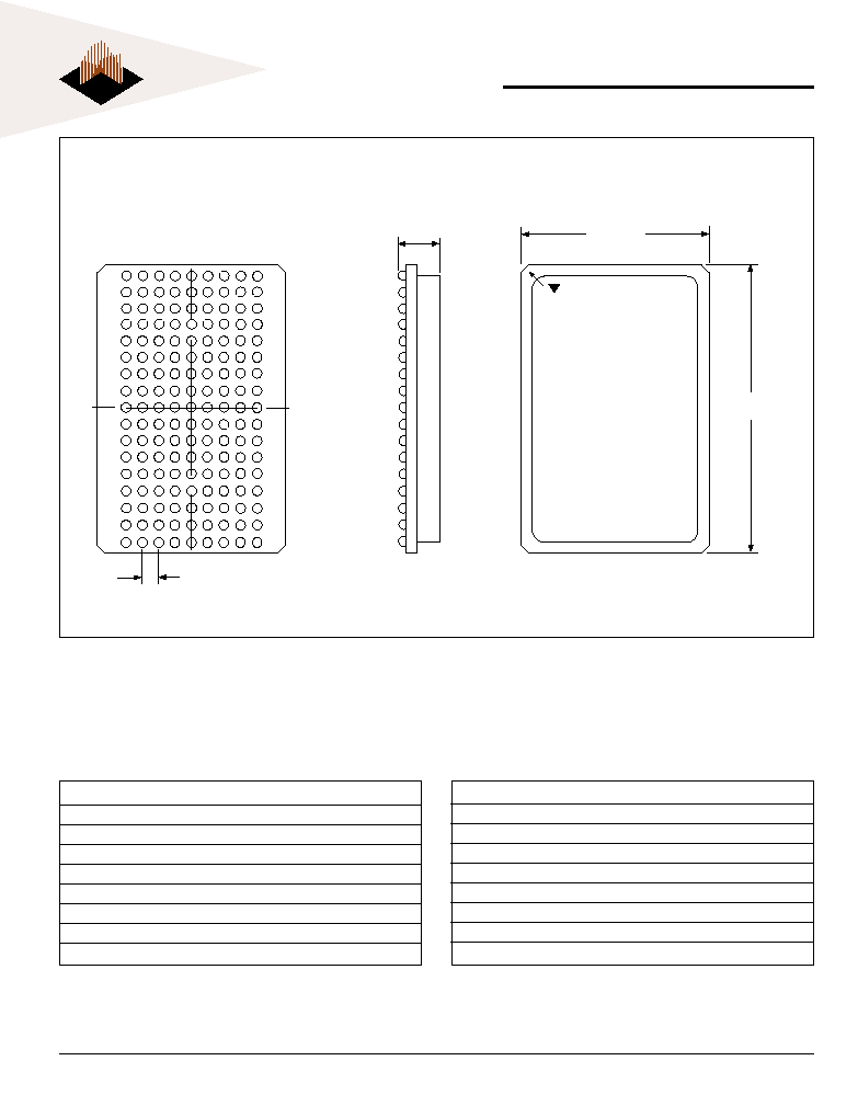
PACKAGE DESCRIPTION: 153 LEAD BGA (17 X 9 BALL ARRAY)
JEDEC MP-163
3.50 (0.138)
MAX
1.27 (0.050) TYP
A
B
C
D
E
F
G
H
J
K
L
M
N
P
R
T
U
14.00 (0.551)
BSC
PIN 1 INDEX
22.00 (0.866)
BSC
ALL LINEAR DIMENSIONS ARE MILLIMETERS AND PARENTHETICALLY IN INCHES
NOTE:
Ball attach pad for above BGA package is 480 microns in diameter. Pad is solder mask defined.
O
RDERING
I
NFORMATION
C
OMMERCIAL
(0�C � TA � 70�C)
I
NDUSTRIAL
(-40�C � TA � 85�C)
Part Number
SSRAM Access
SDRAM Access
WED9LC6816V2012BC
200MHz
125MHz
WED9LC6816V2010BC
200MHz
100MHz
WED9LC6816V1612BC
166MHz
125MHz
WED9LC6816V1610BC
166MHz
100MHz
WED9LC6816V1512BC
150MHz
125MHz
WED9LC6816V1510BC
150MHz
100MHz
WED9LC6816V1312BC
133MHz
125MHz
WED9LC6816V1310BC
133MHz
100MHz
Part Number
SSRAM Access
SDRAM Access
WED9LC6816V2012BI
200MHz
125MHz
WED9LC6816V2010BI
200MHz
100MHz
WED9LC6816V1612BI
166MHz
125MHz
WED9LC6816V1610BI
166MHz
100MHz
WED9LC6816V1512BI
150MHz
125MHz
WED9LC6816V1510BI
150MHz
100MHz
WED9LC6816V1312BI
133MHz
125MHz
WED9LC6816V1310BI
133MHz
100MHz
27
White Electronic Designs Corporation (508) 366-5151 www.whiteedc.com
White Electronic Designs
WED9LC6816V
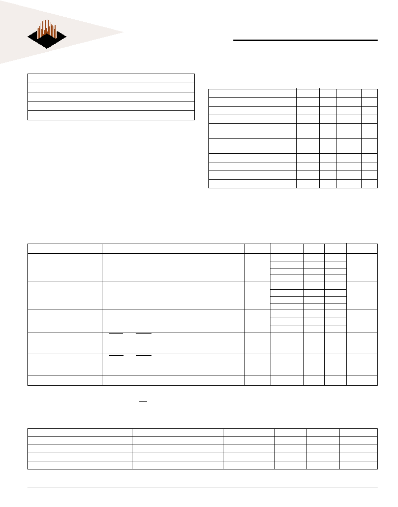
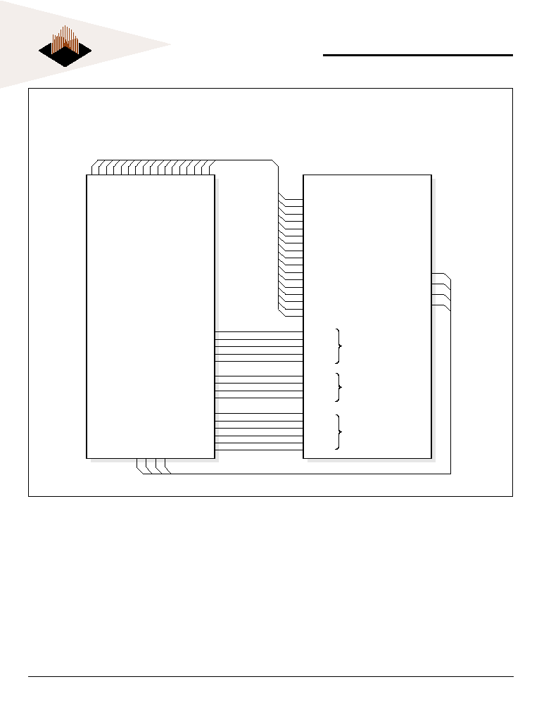
INTERFACING THE TEXAS INSTRUMENTS TMS 320C6x WITH THE
WED9LC6816V (256Kx32 SSRAM/4Mx32 SDRAM)
A
0
A
1
A
2
A
3
A
4
A
5
A
6
A
7
A
8
A
9
A
10
A
11
A
12
A
13
A
14
A
15
A
16
SSWE\
SSCE\
SSOE\
SSADC\
SSCLK
BWE
0
\
BWE
1
\
BWE
2
\
BWE
3
\
SDA
10
SDCE\
SDRAS\
SDCAS\
SDWE\
SDCLK
SSWE\
CE
2
\
SSOE\
SSADS\
SSCLK
BE
0
\
BE
1
\
BE
2
\
BE
3
\
SDA
10
CE
0
\
SDRAS\
SDCAS\
SDWE\
SDCLK
DQ
0-7
DQ
8-15
DQ
16-23
DQ
24-31
Address Bus
EA
2-21
Data Bus
ED
0-31
Texas Instruments
TMS320C6x
DSP
EDI9LC644V
128K x 32 SSRAM
1M x 32 SDRAM
SSRAM
Control
SDRAM
Control
Shared
Controls
EA
2
EA
3