
1
1
1
1
1
White Electronic Designs Corporation ∑ (602) 437-1520 ∑ www.whiteedc.com
WEDPN16M64VR-XBX
November 2003 Rev. 4
GENERAL DESCRIPTION
The 128MByte (1Gb) SDRAM is a high-speed CMOS, dynamic
random-access, memory using 4 chips containing 268,435,456
bits. Each chip is internally configured as a quad-bank DRAM
with a synchronous interface. Each of the chip's 67,108,864-
bit banks is organized as 8,192 rows by 512 columns by 16
bits. The MCP also incorporates two 16-bit universal bus
drivers for input control signals and addresses.
Read and write accesses to the SDRAM are burst oriented;
accesses start at a selected location and continue for a
programmed number of locations in a programmed se-
quence. Accesses begin with the registration of an ACTIVE
command, which is then followed by a READ or WRITE
command. The address bits registered coincident with the
ACTIVE command are used to select the bank and row to be
accessed (BA0, BA1 select the bank; A0-12 select the row).
The address bits registered coincident with the READ or
WRITE command are used to select the starting column
location for the burst access.
The SDRAM provides for programmable READ or WRITE burst
lengths of 1, 2, 4 or 8 locations, or the full page, with a burst
terminate option. An AUTO PRECHARGE function may be
enabled to provide a self-timed row precharge that is initiated
at the end of the burst sequence.
The 1Gb SDRAM uses an internal pipelined architecture to
achieve high-speed operation. This architecture is compat-
ible with the 2
n rule of prefetch architectures, but it also
allows the column address to be changed on every clock
cycle to achieve a high-speed, fully random access. Precharging
one bank while accessing one of the other three banks will
hide the precharge cycles and provide seamless, high-
speed, random-access operation.
The 1Gb SDRAM is designed to operate in 3.3V, low-power
memory systems. An auto refresh mode is provided, along
with a power-saving, power-down mode.
All inputs and outputs are LVTTL compatible. SDRAMs offer
substantial advances in DRAM operating performance, in-
cluding the ability to synchronously burst data at a high data
rate with automatic column-address generation, the ability to
interleave between internal banks in order to hide precharge
time and the capability to randomly change column ad-
dresses on each clock cycle during a burst access.
16MX64 REGISTERED SYNCHRONOUS DRAM
FEATURES
! Registered for enhanced performace of bus speeds
∑ 66, 100, 125, 133** MHz
! Package:
∑ 219 Plastic Ball Grid Array (PBGA), 32 x 25mm
! Single 3.3V ±0.3V power supply
! Fully Synchronous; all signals registered on positive edge
of system clock cycle
! Internal pipelined operation; column address can be
changed every clock cycle
! Internal banks for hiding row access/precharge
! Programmable Burst length 1,2,4,8 or full page
! 8,192 refresh cycles
! Commercial, Industrial and Military Temperature Ranges
! Organized as 16M x 64
∑ User configureable as 32M x 32
! Weight: WEDPN16M64VR-XBX - 2.5 grams typical
BENEFITS
! 37% SPACE SAVINGS
! 17% I/O Reduction
! Reduced part count
! Reduced trace lengths for lower parasitic capacitance
! Glue-less connection to memory controller/PCI Bridge
! Suitable for hi-reliability applications
! Laminate interposer for optimum TCE match
! Upgradeable to 32M x 64 density (contact factory for
information)
*This data sheet describes a product that is subject to change without notice.
**Available in commercial and industrial temperatures only.
White Electronic Designs Corporation ∑ (602) 437-1520 ∑ www.whiteedc.com
WEDPN16M64VR-XBX
2
2
2
2
2
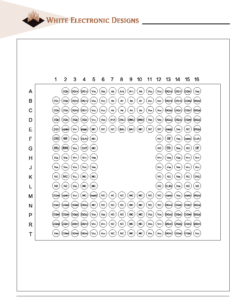
F
IG
. 1 P
IN
C
ONFIGURATION
NOTE: DNU = Do Not Use; to be left unconnected for future upgrades.
NC = Not Connected Internally.
T
OP
V
IEW
3
3
3
3
3
White Electronic Designs Corporation ∑ (602) 437-1520 ∑ www.whiteedc.com
WEDPN16M64VR-XBX
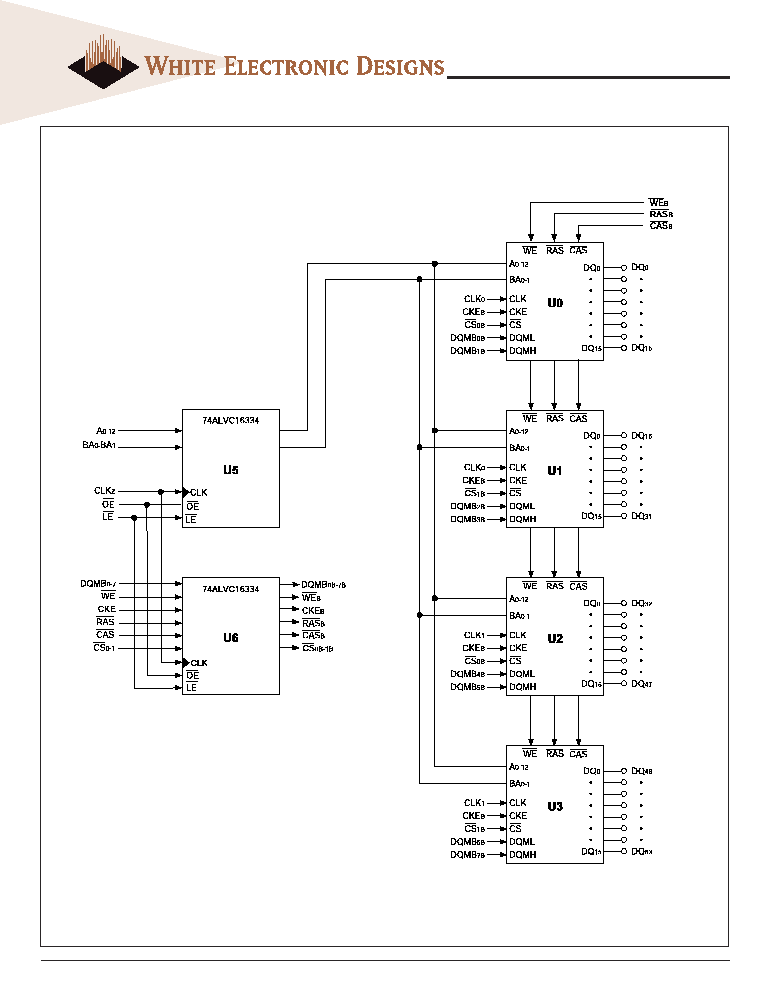
F
IG
. 2 F
UNCTIONAL
B
LOCK
D
IAGRAM

White Electronic Designs Corporation ∑ (602) 437-1520 ∑ www.whiteedc.com
WEDPN16M64VR-XBX
4
4
4
4
4
FUNCTIONAL DESCRIPTION
Read and write accesses to the SDRAM are burst oriented;
accesses start at a selected location and continue for a
programmed number of locations in a programmed se-
quence. Accesses begin with the registration of an ACTIVE
command which is then followed by a READ or WRITE
command. The address bits registered coincident with the
ACTIVE command are used to select the bank and row to be
accessed (BA0 and BA1 select the bank, A0-12 select the
row). The address bits (A0-8) registered coincident with the
READ or WRITE command are used to select the starting
column location for the burst access.
Prior to normal operation, the SDRAM must be initialized. The
following sections provide detailed information covering
device initialization, register definition, command descrip-
tions and device operation.
INITIALIZATION
SDRAMs must be powered up and initialized in a predefined
manner. Operational procedures other than those specified
may result in undefined operation. Once power is applied to
VDD and VDDQ (simultaneously) and the clock is stable
(stable clock is defined as a signal cycling within timing
constraints specified for the clock pin), the SDRAM requires
a 100µs delay prior to issuing any command other than a
COMMAND INHIBIT or a NOP. Starting at some point during
this 100µs period and continuing at least through the end of
this period, COMMAND INHIBIT or NOP commands should
be applied.
Once the 100µs delay has been satisfied with at least one
COMMAND INHIBIT or NOP command having been applied,
a PRECHARGE command should be applied. All banks must
be precharged, thereby placing the device in the all banks idle
state.
Once in the idle state, two AUTO REFRESH cycles must be
performed. After the AUTO REFRESH cycles are complete, the
SDRAM is ready for Mode Register programming. Because the
Mode Register will power up in an unknown state, it should be
loaded prior to applying any operational command.
REGISTER DEFINITION
MODE REGISTER
The Mode Register is used to define the specific mode of
operation of the SDRAM. This definition includes the selec-
tion of a burst length, a burst type, a CAS latency, an operating
mode and a write burst mode, as shown in Figure 3. The Mode
Register is programmed via the LOAD MODE REGISTER com-
mand and will retain the stored information until it is pro-
grammed again or the device loses power.
Mode register bits M0-M2 specify the burst length, M3 speci-
fies the type of burst (sequential or interleaved), M4-M6
specify the CAS latency, M7 and M8 specify the operating
mode, M9 specifies the WRITE burst mode, and M10 and M11
are reserved for future use. Address A12 (M12) is undefined
but should be driven LOW during loading of the mode register.
The Mode Register must be loaded when all banks are idle,
and the controller must wait the specified time before
initiating the subsequent operation. Violating either of these
requirements will result in unspecified operation.
BURST LENGTH
Read and write accesses to the SDRAM are burst oriented,
with the burst length being programmable, as shown in Figure
3. The burst length determines the maximum number of
column locations that can be accessed for a given READ or
WRITE command. Burst lengths of 1, 2, 4 or 8 locations are
available for both the sequential and the interleaved burst
types, and a full-page burst is available for the sequential type.
The full-page burst is used in conjunction with the BURST
TERMINATE command to generate arbitrary burst lengths.
Reserved states should not be used, as unknown operation
or incompatibility with future versions may result.
When a READ or WRITE command is issued, a block of
columns equal to the burst length is effectively selected. All
accesses for that burst take place within this block, meaning
that the burst will wrap within the block if a boundary is
reached. The block is uniquely selected by A1-8 when the
burst length is set to two; by A2-8 when the burst length is
set to four; and by A3-8 when the burst length is set to eight.
The remaining (least significant) address bit(s) is (are) used
to select the starting location within the block. Full-page
bursts wrap within the page if the boundary is reached.
BURST TYPE
Accesses within a given burst may be programmed to be
either sequential or interleaved; this is referred to as the burst
type and is selected via bit M3.
The ordering of accesses within a burst is determined by the
burst length, the burst type and the starting column address,
as shown in Table 1.
5
5
5
5
5
White Electronic Designs Corporation ∑ (602) 437-1520 ∑ www.whiteedc.com
WEDPN16M64VR-XBX
T
ABLE
1 - B
URST
D
EFINITION
Burst
Starting Column
Order of Accesses Within a Burst
Length
Address
A0
2
0
0-1
0-1
1
1-0
1-0
A1
A0
0
0
0-1-2-3
0-1-2-3
4
0
1
1-2-3-0
1-0-3-2
1
0
2-3-0-1
2-3-0-1
1
1
3-0-1-2
3-2-1-0
A2
A1
A0
0
0
0
0-1-2-3-4-5-6-7
0-1-2-3-4-5-6-7
0
0
1
1-2-3-4-5-6-7-0
1-0-3-2-5-4-7-6
0
1
0
2-3-4-5-6-7-0-1
2-3-0-1-6-7-4-5
8
0
1
1
3-4-5-6-7-0-1-2
3-2-1-0-7-6-5-4
1
0
0
4-5-6-7-0-1-2-3
4-5-6-7-0-1-2-3
1
0
1
5-6-7-0-1-2-3-4
5-4-7-6-1-0-3-2
1
1
0
6-7-0-1-2-3-4-5
6-7-4-5-2-3-0-1
1
1
1
7-0-1-2-3-4-5-6
7-6-5-4-3-2-1-0
Full
n = A0-9/8/7
Cn, Cn + 1, Cn + 2
Page
Cn + 3, Cn + 4...
Not Supported
(y)
(location 0-y)
...Cn - 1,
Cn...
NOTES:
NOTES:
NOTES:
NOTES:
NOTES:
1. For full-page accesses: y = 512.
2. For a burst length of two, A1-8 select the block-of-two burst; A0 selects
the starting column within the block.
3. For a burst length of four, A2-8 select the block-of-four burst; A0-1 select
the starting column within the block.
4. For a burst length of eight, A3-8 select the block-of-eight burst; A0-2
select the starting column within the block.
5. For a full-page burst, the full row is selected and A0-8 select the starting
column.
6. Whenever a boundary of the block is reached within a given sequence
above, the following access wraps within the block.
7. For a burst length of one, A0-8 select the unique column to be accessed,
and Mode Register bit M3 is ignored.
Type = Sequential Type = Interleaved
M3 = 0
1
2
4
8
Reserved
Reserved
Reserved
Full Page
M3 = 1
1
2
4
8
Reserved
Reserved
Reserved
Reserved
Operating Mode
Standard Operation
All other states reserved
0
-
0
-
Defined
-
0
1
Burst Type
Sequential
Interleaved
CAS Latency
Reserved
Reserved
2
3
Reserved
Reserved
Reserved
Reserved
Burst Length
M0
0
1
0
1
0
1
0
1
Burst Length
CAS Latency
BT
A
9
A
7
A
6
A
5
A
4
A
3
A
8
A
2
A
1
A
0
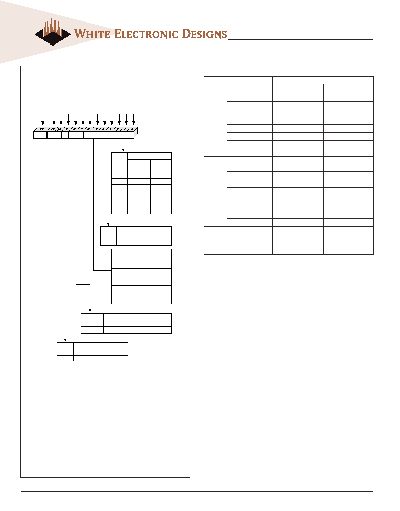
Mode Register (Mx)
Address Bus
M1
0
0
1
1
0
0
1
1
M2
0
0
0
0
1
1
1
1
M3
M4
0
1
0
1
0
1
0
1
M5
0
0
1
1
0
0
1
1
M6
0
0
0
0
1
1
1
1
M6-M0
M8
M7
Op Mode
A
10
A
11
Reserved* WB
0
1
Write Burst Mode
Programmed Burst Length
Single Location Access
M9
*Should program
M12, M11, M10 = 0, 0, 0
to ensure compatibility
with future devices.
Unused
WEDPN16M72MRD.eps
A
12
F
IG
. 1 M
ODE
R
EGISTER
D
EFINITION
White Electronic Designs Corporation ∑ (602) 437-1520 ∑ www.whiteedc.com
WEDPN16M64VR-XBX
6
6
6
6
6
ALLOWABLE OPERATING
FREQUENCY (MHZ)
CAS
CAS
SPEED
LATENCY = 2
LATENCY = 3
-133
100
133
-125
100
125
-100
66
100
-66
50
66
CAS LATENCY
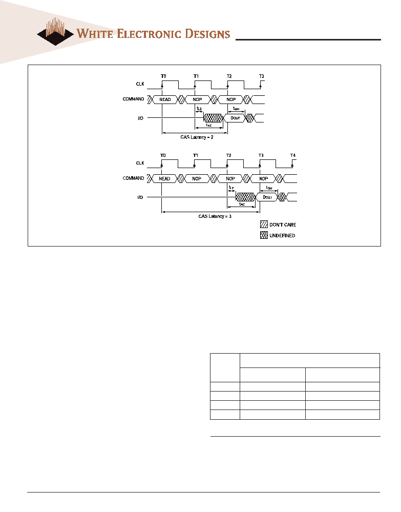
The CAS latency is the delay, in clock cycles, between the
registration of a READ command and the availability of the first
piece of output data. The latency can be set to two or three
clocks.
If a READ command is registered at clock edge
n, and the
latency is
m clocks, the data will be available by clock edge
n+m. The I/Os will start driving as a result of the clock edge
one cycle earlier (
n + m - 1), and provided that the relevant
access times are met, the data will be valid by clock edge
n
+ m. For example, assuming that the clock cycle time is such
that all relevant access times are met, if a READ command is
registered at T0 and the latency is programmed to two clocks,
the I/Os will start driving after T1 and the data will be valid by
T2. Table 2 below indicates the operating frequencies at
which each CAS latency setting can be used.
Reserved states should not be used as unknown operation
or incompatibility with future versions may result.
OPERATING MODE
The normal operating mode is selected by setting M7and M8
to zero; the other combinations of values for M7 and M8 are
reserved for future use and/or test modes. The programmed
burst length applies to both READ and WRITE bursts.
Test modes and reserved states should not be used because
unknown operation or incompatibility with future versions
may result.
WRITE BURST MODE
When M9 = 0, the burst length programmed via M0-M2
applies to both READ and WRITE bursts; when M9 = 1, the
programmed burst length applies to READ bursts, but write
accesses are single-location (nonburst) accesses
COMMANDS
The Truth Table provides a quick reference of available
commands. This is followed by a written description of each
command. Three additional Truth Tables appear following
the Operation section; these tables provide current state/
next state information.
F
IG
. 4 C
AS
L
ATENCY
T
ABLE
2 - C
AS
L
ATENCY
7
7
7
7
7
White Electronic Designs Corporation ∑ (602) 437-1520 ∑ www.whiteedc.com
WEDPN16M64VR-XBX
TRUTH TABLE - COMMANDS AND DQM OPERATION
(N
OTE
1)
NAME (FUNCTION)
CS
RAS
CAS
WE
DQM
ADDR
I/Os
COMMAND INHIBIT (NOP)
H
X
X
X
X
X
X
NO OPERATION (NOP)
L
H
H
H
X
X
X
ACTIVE (Select bank and activate row) ( 3)
L
L
H
H
X
Bank/Row
X
READ (Select bank and column, and start READ burst) (4)
L
H
L
H
L/H
8
Bank/Col
X
WRITE (Select bank and column, and start WRITE burst) (4)
L
H
L
L
L/H
8
Bank/Col
Valid
BURST TERMINATE
L
H
H
L
X
X
Active
PRECHARGE (Deactivate row in bank or banks) ( 5)
L
L
H
L
X
Code
X
AUTO REFRESH or SELF REFRESH (Enter self refresh mode) (6, 7)
L
L
L
H
X
X
X
LOAD MODE REGISTER (2)
L
L
L
L
X
Op-Code
X
Write Enable/Output Enable (8)
≠
≠
≠
≠
L
≠
Active
Write Inhibit/Output High-Z (8)
≠
≠
≠
≠
H
≠
High-Z
NOTES:
1. CKE is HIGH for all commands shown except SELF REFRESH.
2. A0-11 define the op-code written to the Mode Register.
3. A0-12 provide row address, and BA0, BA1 determine which bank is made active.
4. A0-8 provide column address; A10 HIGH enables the auto precharge feature (nonpersistent), while A10 LOW disables the auto precharge feature; BA0, BA1
determine which bank is being read from or written to.
5. A10 LOW: BA0, BA1 determine the bank being precharged. A10 HIGH: All banks precharged and BA0, BA1 are "Don't Care."
6. This command is AUTO REFRESH if CKE is HIGH; SELF REFRESH if CKE is LOW.
7. Internal refresh counter controls row addressing; all inputs and I/Os are "Don't Care" except for CKE.
8. Activates or deactivates the I/Os during WRITEs (zero-clock delay) and READs (two-clock delay).
LOAD MODE REGISTER
The Mode Register is loaded via inputs A0-11. See Mode
Register heading in the Register Definition section. The LOAD
MODE REGISTER command can only be issued when all
banks are idle, and a subsequent executable command
cannot be issued until tMRD is met.
ACTIVE
The ACTIVE command is used to open (or activate) a row in
a particular bank for a subsequent access. The value on the
BA0, BA1 inputs selects the bank, and the address provided
on inputs A0-A12 selects the row. This row remains active
(or open) for accesses until a PRECHARGE command is
issued to that bank. A PRECHARGE command must be issued
before opening a different row in the same bank.
READ
The READ command is used to initiate a burst read access to
an active row. The value on the BA0, BA1 inputs selects the
bank, and the address provided on inputs A0-8 selects the
starting column location. The value on input A10 determines
whether or not AUTO PRECHARGE is used. If AUTO PRECHARGE
is selected, the row being accessed will be precharged at the
end of the READ burst; if AUTO PRECHARGE is not selected,
COMMAND INHIBIT
The COMMAND INHIBIT function prevents new commands
from being executed by the SDRAM, regardless of whether
the CLK signal is enabled. The SDRAM is effectively dese-
lected. Operations already in progress are not affected.
NO OPERATION (NOP)
The NO OPERATION (NOP) command is used to perform a
NOP to an SDRAM which is selected (CS is LOW). This prevents
unwanted commands from being registered during idle or wait
states. Operations already in progress are not affected.
INPUTS
OUTPUT
OE
LE
CLK
A
Y
H
X
X
X
Z
L
L
X
L
L
L
L
X
H
H
L
H
I
L
L
L
H
I
H
H
L
H
L or H
X
Y
0
(1)
NOTES:
1. Output level before the indicated steady-state input
conditions were established.
R
EGISTER
F
UNCTION
T
ABLE

White Electronic Designs Corporation ∑ (602) 437-1520 ∑ www.whiteedc.com
WEDPN16M64VR-XBX
8
8
8
8
8
the row will remain open for subsequent accesses. Read data
appears on the I/Os subject to the logic level on the DQM
inputs two clocks earlier. If a given DQM signal was registered
HIGH, the corresponding I/Os will be High-Z two clocks later;
if the DQM signal was registered LOW, the I/Os will provide
valid data.
WRITE
The WRITE command is used to initiate a burst write access
to an active row. The value on the BA0, BA1 inputs selects the
bank, and the address provided on inputs A0-8 selects the
starting column location. The value on input A10 determines
whether or not AUTO PRECHARGE is used. If AUTO PRECHARGE
is selected, the row being accessed will be precharged at the
end of the WRITE burst; if AUTO PRECHARGE is not selected,
the row will remain open for subsequent accesses. Input data
appearing on the I/Os is written to the memory array subject
to the DQM input logic level appearing coincident with the
data. If a given DQM signal is registered LOW, the correspond-
ing data will be written to memory; if the DQM signal is
registered HIGH, the corresponding data inputs will be
ignored, and a WRITE will not be executed to that byte/
column location.
PRECHARGE
The PRECHARGE command is used to deactivate the open
row in a particular bank or the open row in all banks. The
bank(s) will be available for a subsequent row access a
specified time (tRP) after the PRECHARGE command is issued.
Input A10 determines whether one or all banks are to be
precharged, and in the case where only one bank is to be
precharged, inputs BA0, BA1 select the bank. Otherwise
BA0, BA1 are treated as "Don't Care." Once a bank has been
precharged, it is in the idle state and must be activated prior
to any READ or WRITE commands being issued to that bank.
AUTO PRECHARGE
AUTO PRECHARGE is a feature which performs the same
individual-bank PRECHARGE function described above, without
requiring an explicit command. This is accomplished by using
A10 to enable AUTO PRECHARGE in conjunction with a
specific READ or WRITE command. A precharge of the bank/
row that is addressed with the READ or WRITE command is
automatically performed upon completion of the READ or
WRITE burst, except in the full-page burst mode, where
AUTO PRECHARGE does not apply. AUTO PRECHARGE is
nonpersistent in that it is either enabled or disabled for each
individual READ or WRITE command.
AUTO PRECHARGE ensures that the precharge is initiated at the
earliest valid stage within a burst. The user must not issue
another command to the same bank until the precharge time
(tRP) is completed. This is determined as if an explicit PRECHARGE
command was issued at the earliest possible time.
BURST TERMINATE
The BURST TERMINATE command is used to truncate either
fixed-length or full-page bursts. The most recently registered
READ or WRITE command prior to the BURST TERMINATE
command will be truncated.
AUTO REFRESH
AUTO REFRESH is used during normal operation of the SDRAM
and is analagous to CAS-BEFORE-RAS (CBR) REFRESH in
conventional DRAMs. This command is nonpersistent, so it
must be issued each time a refresh is required.
The addressing is generated by the internal refresh controller.
This makes the address bits "Don't Care" during an AUTO
REFRESH command. Each 256Mb SDRAM requires 8,192
AUTO REFRESH cycles every refresh period (tREF). Providing
a distributed AUTO REFRESH command will meet the refresh
requirement and ensure that each row is refreshed. Alterna-
tively, 8,192 AUTO REFRESH commands can be issued in a
burst at the minimum cycle rate (tRC), once every refresh
period (tREF).
SELF REFRESH*
The SELF REFRESH command can be used to retain data in the
SDRAM, even if the rest of the system is powered down.
When in the self refresh mode, the SDRAM retains data
without external clocking. The SELF REFRESH command is
initiated like an AUTO REFRESH command except CKE is
disabled (LOW). Once the SELF REFRESH command is regis-
tered, all the inputs to the SDRAM become "Don't Care," with
the exception of CKE, which must remain LOW.
Once self refresh mode is engaged, the SDRAM provides its
own internal clocking, causing it to perform its own AUTO
REFRESH cycles. The SDRAM must remain in self refresh mode
for a minimum period equal to tRAS and may remain in self
refresh mode for an indefinite period beyond that.
9
9
9
9
9
White Electronic Designs Corporation ∑ (602) 437-1520 ∑ www.whiteedc.com
WEDPN16M64VR-XBX
DC E
LECTRICAL
C
HARACTERISTICS
A
ND
O
PERATING
C
ONDITIONS
(N
OTES
1, 6)
(VCC = +3.3V ±0.3V; TA = -55∞C
TO
+125∞C)
Parameter/Condition
Symbol
Units
Min
Max
Supply Voltage
V
CC
3
3.6
V
Input High Voltage: Logic 1; All inputs (21)
V
IH
2
V
CC
+ 0.3
V
Input Low Voltage: Logic 0; All inputs (21)
V
IL
-0.3
0.8
V
Input Leakage Current: Any input 0V - V
IN
- V
CC
(All other pins not under test = 0V)
I
I
-5
5
µA
Output Leakage Current: I/Os are disabled; 0V - V
OUT
- V
CC
I
OZ
-5
5
µA
Output High Voltage (I
OUT
= -4mA)
V
OH
2.4
≠
V
Output Low Voltage (I
OUT
= 4mA)
V
OL
≠
0.4
V
A
BSOLUTE
M
AXIMUM
R
ATINGS
Parameter
Unit
Voltage on V
DD
, V
DDQ
Supply relative to Vss
-1 to 4.6
V
Voltage on NC or I/O pins relative to Vss
-1 to 4.6
V
Operating Temperature T
A
(Mil)
-55 to +125
∞C
Operating Temperature T
A
(Ind)
-40 to +85
∞C
Storage Temperature, Plastic
-55 to +150
∞C
NOTE: Stress greater than those listed under "Absolute Maximum Ratings" may
cause permanent damage to the device. This is a stress rating only and
functional operation of the device at these or any other conditions greater than
those indicated in the operational sections of this specification is not implied.
Exposure to absolute maximum rating conditions for extended periods may
affect reliability.
Parameter
Symbol
Max
Unit
Input Capacitance: CLK
C
I1
20
pF
Addresses, BA
0-1
Input Capacitance
CA
8
pF
Input Capacitance: All other input-only pins
C
I2
10
pF
Input/Output Capacitance: I/Os
C
IO
10
pF
ICC S
PECIFICATIONS
A
ND
C
ONDITIONS
(N
OTES
1,6,11,13)
(VCC = +3.3V ±0.3V; TA = -55∞C
TO
+125∞C)
Parameter/Condition
Symbol
Max
Units
Operating Current: Active Mode;
I
CC1
700
mA
Burst = 2; Read or Write; t
RC
= t
RC
(min); CAS latency = 3 (3, 18, 19)
Standby Current: Active Mode; CKE = HIGH; CS = HIGH;
I
CC3
240
mA
All banks active after t
RCD
met; No accesses in progress (3, 12, 19)
Operating Current: Burst Mode; Continuous burst;
I
CC4
750
mA
Read or Write; All banks active; CAS latency = 3 (3, 18, 19)
Self Refresh Current: CKE - 0.2V (27, 28)
I
CC7
20
mA
The procedure for exiting self refresh requires a sequence of
commands. First, CLK must be stable (stable clock is defined
as a signal cycling within timing constraints specified for the
clock pin) prior to CKE going back HIGH. Once CKE is HIGH,
the SDRAM must have NOP commands issued (a minimum of
two clocks) for tXSR, because time is required for the
completion of any internal refresh in progress.
Upon exiting the self refresh mode, AUTO REFRESH com-
mands must be issued as both SELF REFRESH and AUTO
REFRESH utilize the row refresh counter.
* Self refresh available in commercial and industrial temperatures only.
C
APACITANCE
(N
OTE
2)
Description
Symbol
Max
Unit
Notes
Junction to Ambient (No Airflow)
Theta JA
14.7
∫C/W
1
Junction to Bail
Theta JB
10.7
∫C/W
1
Junction to Case (Top)
Theta JC
4.0
∫C/W
1
BGA T
HERMAL
R
ESISTANCE
NOTE:
Refer to PBGA Thermal Resistance Correlation Application note at
www.whiteedc.com in the application notes section for modeling conditions.
White Electronic Designs Corporation ∑ (602) 437-1520 ∑ www.whiteedc.com
WEDPN16M64VR-XBX
10
10
10
10
10
Parameter
Symbol -133
-125
-100 -66
Unit
Min
Max
Min
Max
Min
Max
Min
Max
Access time from CLK (pos. edge)
CL = 3
t
AC
5.4
5.8
6
7.5
ns
CL = 2
t
AC
6
6
6
9
ns
Address hold time
t
AH
0.8
1
1
1
ns
Address setup time
t
AS
1.5
2
2
2
ns
CLK high-level width
t
CH
2.5
3
3
3
ns
CLK low-level width
t
CL
2.5
3
3
3
ns
Clock cycle time (22)
CL = 3
t
CK
7.5
8
10
15
ns
CL = 2
t
CK
10
10
15
20
ns
CKE hold time
t
CKH
0.8
1
1
1
ns
CKE setup time
t
CKS
1.5
2
2
2
ns
CS, RAS, CAS, WE, DQM hold time
t
CMH
0.8
1
1
1
ns
CS, RAS, CAS, WE, DQM setup time
t
CMS
1.5
2
2
2
ns
Data-in hold time
t
DH
0.8
1
1
1
ns
Data-in setup time
t
DS
1.5
2
2
2
ns
Data-out high-impedance time
CL = 3 (10)
t
HZ
5.4
5.8
6
7.5
ns
CL = 2 (10)
t
HZ
6
6
6
9
ns
Data-out low-impedance time
t
LZ
1
1
1
2
ns
Data-out hold time (load)
t
OH
3
3
3
3
ns
Data-out hold time (no load) (26)
t
OH
N
1.8
1.8
1.8
1.8
ns
ACTIVE to PRECHARGE command
t
RAS
44
120,000
50
120,000
50
120,000
60
120,000
ns
ACTIVE to ACTIVE command period
t
RC
66
70
70
70
ns
ACTIVE to READ or WRITE delay
t
RCD
20
20
20
30
ns
Refresh period (8,192 rows) ≠ Commercial, Industrial
t
REF
64
64
64
64
ms
Refresh period (8,192 rows) ≠ Military
t
REF
16
16
16
16
ms
AUTO REFRESH period
t
RFC
66
70
70
90
ns
PRECHARGE command period
t
RP
20
20
20
30
ns
ACTIVE bank A to ACTIVE bank B command
t
RRD
15
20
20
20
ns
Transition time (7)
t
T
0.3
1.2
0.3
1.2
0.3
1.2
1
1.2
ns
WRITE recovery time (23)
t
WR
1CLK + 7.5ns
1CLK + 7.5ns
1 CLK + 7.5ns
1 CLK + 7.5ns
--
(24)
15
15
15
15
ns
Exit SELF REFRESH to ACTIVE command
t
XSR
75
80
80
90
ns
E
LECTRICAL
C
HARACTERISTICS
A
ND
R
ECOMMENDED
AC O
PERATING
C
HARACTERISTICS
(N
OTES
5, 6, 8, 9, 11, 29)
11
11
11
11
11
White Electronic Designs Corporation ∑ (602) 437-1520 ∑ www.whiteedc.com
WEDPN16M64VR-XBX
AC F
UNCTIONAL
C
HARACTERISTICS
(N
OTES
5,6,7,8,9,11, 29)
Parameter/Condition
Symbol
-133
-125
-100
-66
Units
READ/WRITE command to READ/WRITE command (17)
t
CCD
1
1
1
1
t
CK
CKE to clock disable or power-down entry mode (14)
t
CKED
1
1
1
1
t
CK
CKE to clock enable or power-down exit setup mode (14)
t
PED
1
1
1
1
t
CK
DQM to input data delay (17)
t
DQD
0
0
0
0
t
CK
DQM to data mask during WRITEs
t
DQM
0
0
0
0
t
CK
DQM to data high-impedance during READs
t
DQZ
2
2
2
2
t
CK
WRITE command to input data delay (17)
t
DWD
0
0
0
0
t
CK
Data-in to ACTIVE command (15)
t
DAL
5
5
4
4
t
CK
Data-in to PRECHARGE command (16)
t
DPL
2
2
2
2
t
CK
Last data-in to burst STOP command (17)
t
BDL
1
1
1
1
t
CK
Last data-in to new READ/WRITE command (17)
t
CDL
1
1
1
1
t
CK
Last data-in to PRECHARGE command (16)
t
RDL
2
2
2
2
t
CK
LOAD MODE REGISTER command to ACTIVE or REFRESH command (25)
t
MRD
2
2
2
2
t
CK
Data-out to high-impedance from PRECHARGE command (17)
CL = 3
t
ROH
3
3
3
3
t
CK
CL = 2
t
ROH
2
2
2
2
t
CK
NOTES:
1. All voltages referenced to VSS.
2. This parameter is not tested but guaranteed by design. f = 1 MHz, TA = 25∞C.
3. IDD is dependent on output loading and cycle rates. Specified values are
obtained with minimum cycle time and the outputs open.
4. Enables on-chip refresh and address counters.
5. The minimum specifications are used only to indicate cycle time at which
proper operation over the full temperature range is ensured.
6. An initial pause of 100µs is required after power-up, followed by two
AUTO REFRESH commands, before proper device operation is ensured. (VCC
must be powered up simultaneously.) The two AUTO REFRESH command
wake-ups should be repeated any time the tREF refresh requirement is
exceeded.
7. AC characteristics assume tT = 1ns.
8. In addition to meeting the transition rate specification, the clock and CKE
must transit between VIH and VIL (or between VIL and VIH) in a monotonic
manner.
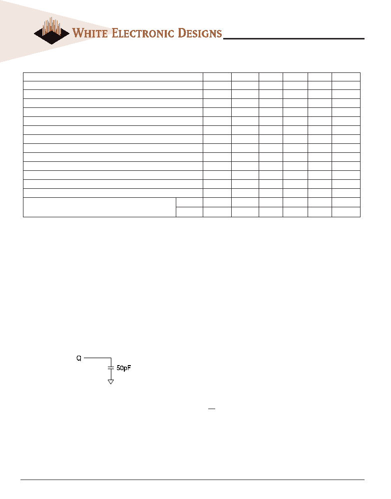
9. Outputs measured at 1.5V with equivalent load:
10. tHZ defines the time at which the output achieves the open circuit
condition; it is not a reference to VOH or VOL. The last valid data element will
meet tOH before going High-Z.
11. AC timing and IDD tests have VIL = 0V and VIH = 3V, with timing
referenced to 1.5V crossover point.
12. Other input signals are allowed to transition no more than once every two
clocks and are otherwise at valid VIH or VIL levels.
13. ICC specifications are tested after the device is properly initialized.
14. Timing actually specified by tCKS; clock(s) specified as a reference only
at minimum cycle rate.
15. Timing actually specified by tWR plus tRP; clock(s) specified as a
reference only at minimum cycle rate.
16. Timing actually specified by tWR.
17. Required clocks are specified by JEDEC functionality and are not
dependent on any timing parameter.
18. The ICC current will decrease as the CAS latency is reduced. This is due to
the fact that the maximum cycle rate is slower as the CAS latency is reduced.
19. Address transitions average one transition every two clocks.
20. CLK must be toggled a minimum of two times during this period.
21. VIH overshoot: VIH (MAX) = VCC + 2V for a pulse width - 3ns, and the
pulse width cannot be greater than one third of the cycle rate. VIL undershoot:
VIL (MIN) = -2V for a pulse width - 3ns.
22. The clock frequency must remain constant (stable clock is defined as a
signal cycling within timing constraints specified for the clock pin) during
access or precharge states (READ, WRITE, including tWR, and PRECHARGE
commands). CKE may be used to reduce the data rate.
23. Auto precharge mode only. The precharge timing budget (tRP) begins
7.5ns after the first clock delay, after the last WRITE is executed.
24. Precharge mode only.
25. JEDEC and PC100 specify three clocks.
26. Parameter guaranteed by design.
27. Self refresh available in commercial and industrial temperatures only.
28. OE high.
29. All AC timings do not count extra clock cycle needed on control signals
to be registered.
White Electronic Designs Corporation ∑ (602) 437-1520 ∑ www.whiteedc.com
WEDPN16M64VR-XBX
12
12
12
12
12
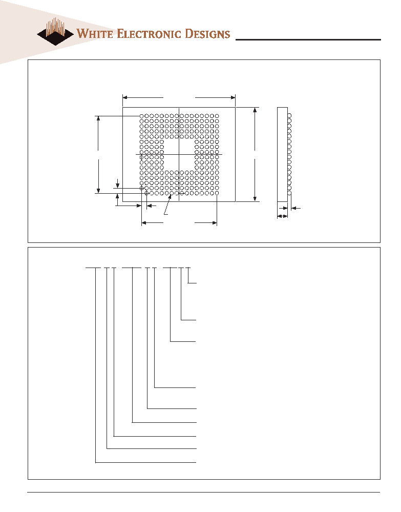
P
ACKAGE
D
IMENSION
: 219 P
LASTIC
B
ALL
G
RID
A
RRAY
(PBGA)
ALL LINEAR DIMENSIONS ARE MILLIMETERS AND PARENTHETICALLY IN INCHES
B
OTTOM
View
O
RDERING
I
NFORMATION
WED P N 16M64 V R - XXX B X
DEVICE GRADE:
M = Military
-55∞C to +125∞C
I = Industrial
-40∞C to +85∞C
C = Commercial
0∞C to +70∞C
PACKAGE:
B = 219 Plastic Ball Grid Array (PBGA)
FREQUENCY (MHz)
133 = 133MHz*
125 = 125MHz
100 = 100MHz
66 = 66MHz
IMPROVEMENT MARK
R = Registered
3.3V Power Supply
CONFIGURATION, 16 M x 64
SDRAM
PLASTIC
WHITE ELECTRONIC DESIGNS CORP.
1 2 3 4 5 6 7 8 9 10 11 12 13 14 15 16
T
R
P
N
M
L
K
J
H
G
F
E
D
C
B
A
219 x
ÿ
0.762 (0.030) NOM
1.27 (0.050)
NOM
32.1 (1.264) MAX
25.1 (0.988)
MAX
2.03 (0.080)
MAX
0.61 (0.024) NOM
19.05 (0.750) NOM
19.05 (0.750)
NOM
*133 MHz available in Commercial and Industrial Temperatures Only

13
13
13
13
13
White Electronic Designs Corporation ∑ (602) 437-1520 ∑ www.whiteedc.com
WEDPN16M64VR-XBX
Document Title
16M x 64 Registered Synchronous DRAM
Revision History
Rev #
History
Release Date
Status
Rev 0
Initial Release
July 2001
Advanced
Rev 1
Changes (Pg. 1, 3, 9, 10, 11)
September 2001
Advanced
1.1
Change speed to 66MHz-133MHz for commercial and industrial temperature.
1.2
Change speed to 66MHz-125MHz for Military temperature.
1.3
Add 125 MHz and 133 MHz AC characteristics
1.4
Correct typo on Pg. 3 Block Diagram, U4 and U5
1.5
Remove Input Leakage Address Current from DC Characteristics
1.6
Change Icc4 to 750mA
1.7
Change Icc7 to 20mA
1.8
Remove Self Refresh Current for Industrial Temperatures
1.9
Update AC Characteristics Pg. 10 and 11
1.10
Add notes 28 and 29 on Pg. 11
Rev 2
Changes (Pg. 1)
1.1
Change status to Preliminary
January 2002
Preliminary
Rev 3
Changes (Pg. 1)
June 2003
Final
1.1
Change Status to Final
1.2
Add Thermal Resistance Table
Rev 4
Changes (Pg. 1, 12, 13)
November 2003
Final
1.1
Change mechanical drawing to new style