1
White Electronic Designs Corporation ∑ (602) 437-1520 ∑ www.wedc.com
WEDPN8M72V-XB2X
White Electronic Designs
January 2005
Rev. 4
White Electronic Designs Corp. reserves the right to change products or specifi cations without notice.
GENERAL DESCRIPTION
The 64MByte (512Mb) SDRAM is a high-speed CMOS,
dy nam ic ran dom-access ,memory using 5 chips containing
134,217,728 bits. Each chip is internally confi gured as a
quad-bank DRAM with a syn chro nous interface. Each of
the chip's 33,554,432-bit banks is or ga nized as 4,096 rows
by 512 columns by 16 bits.
Read and write accesses to the SDRAM are burst oriented;
accesses start at a selected location and continue for
a pro grammed number of locations in a programmed
se quence. Ac cess es begin with the registration of an
ACTIVE com mand, which is then followed by a READ or
WRITE com mand. The address bits registered coincident
with the AC TIVE command are used to select the bank and
row to be accessed (BA0, BA1 select the bank; A0-11 select
the row). The address bits registered co in ci dent with the
READ or WRITE com mand are used to select the starting
column lo ca tion for the burst access.
The SDRAM provides for programmable READ or WRITE
burst lengths of 1, 2, 4 or 8 locations, or the full page, with
a burst terminate option. An AUTO PRECHARGE function
may be en abled to provide a self-timed row precharge that
is initiated at the end of the burst sequence.
The 512Mb SDRAM uses an internal pipelined architecture
to achieve high-speed operation. This architecture is
com pat i ble with the 2n rule of prefetch architectures, but
it also allows the column address to be changed on every
clock cycle to achieve a high-speed, fully random access.
Precharging one bank while accessing one of the other three
banks will hide the precharge cycles and provide seam less,
high-speed, random-access op er a tion.
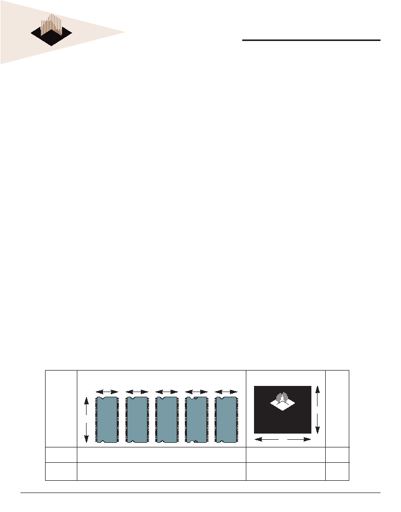
8Mx72 Synchronous DRAM
FEATURES
High
Fre
quen cy = 100, 125, 133MHz
Package:
∑ 219 Plas
tic Ball Grid Ar ray (PBGA), 21 x 25mm
Single 3.3V ± 0.3V pow er sup ply
Fully
Syn
chro nous; all sig nals reg is tered on pos i tive
edge of system clock cycle
Internal pipelined operation; column address can be
changed every clock cycle
Internal banks for hiding row access/precharge
Programmable Burst length 1, 2, 4, 8 or full page
4096 refresh cycles
Commercial,
Industrial
and
Military
Temperature
Rang es
Organized as 8M x 72
Weight: WEDPN8M72V-XB2X - 2 grams typical
BENEFITS
60%
SPACE
SAVINGS
Reduced part count
Reduced
I/O
count
∑ 19% I/O Reduction
Lower inductance and capacitance for low noise
performance
Suitable for hi-reliability applications
Upgradeable to 16M x 72 and 32M x 72 densities
(contact fac to ry for information)
* This product is subject to change without notice.
54
TSOP
54
TSOP
54
TSOP
54
TSOP
54
TSOP
11.9
11.9
11.9
11.9
11.9
22.3
Area
5 x 265mm
2
= 1328mm
2
525mm
2
60%
5 x 54 pins = 270 pins
219 Balls
19%
I/O
Count
White Electronic Designs
WEDPN8M72V-XB2X
21
25
Discrete Approach
Actual Size
S
A
V
I
N
G
S
2
White Electronic Designs Corporation ∑ (602) 437-1520 ∑ www.wedc.com
WEDPN8M72V-XB2X
White Electronic Designs
January 2005
Rev. 4
White Electronic Designs Corp. reserves the right to change products or specifi cations without notice.
1
2
3
4
5
6
7
8
9 10
11 12 13 14 15 16
A
B
C
D
E
F
G
H
J
K
L
M
N
P
R
T
DQ
1
DQ
3
DQ
6
DQ
7
CAS
0
#
CS
0
#
V
SS
V
SS
NC
NC
DQ
56
DQ
57
DQ
60
DQ
62
Vss
V
SS
DQ
30
DQ
28
DQ
25
DQ
24
CLK
1
CKE
1
V
CC
V
CC
CS
2
#
CAS
2
#
DQ
39
DQ
38
DQ
35
DQ
33
V
CC
DQ
0
DQ
2
DQ
4
DQ
5
DQML0
WE
0
#
RAS
0
#
V
SS
V
SS
CKE
3
CLK
3
DQMH3
DQ
58
DQ
59
DQ
61
DQ
63
DQ
31
DQ
29
DQ
27
DQ
26
NC
DQMH1
NC
V
CC
V
CC
RAS
2
#
WE
2
#
DQML2
DQ
37
DQ
36
DQ
34
DQ
32
DQ
14
DQ
12
DQ
10
DQ
8
V
CC
V
CC
V
CC
V
CC
V
CC
V
CC
V
CC
V
CC
DQ
55
DQ
53
DQ
51
DQ
49
DQ
17
DQ
19
DQ
21
DQ
23
V
SS
V
SS
V
SS
Vss
V
SS
V
SS
V
SS
V
SS
DQ
40
DQ
42
DQ
44
DQ
46
DQ
15
DQ
13
DQ
11
DQ
9
DQMH0
CLK
0
CKE
0
V
CC
V
CC
CS
3
#
CAS
3
#
WE
3
#
DQ
54
DQ
52
DQ
50
DQ
48
DQ
16
DQ
18
DQ
20
DQ
22
DQML1
WE
1
#
CS
1
#
V
SS
V
SS
CKE
2
CLK
2
DQMH2
DQ
41
DQ
43
DQ
45
DQ
47
V
SS
V
SS
V
CC
V
CC
NC
NC
NC
V
SS
V
SS
NC
RAS
3
#
DQML3
NC
V
SS
V
CC
V
CC
V
CC
V
CC
V
SS
V
SS
NC
RAS
1
#
CAS
1
#
V
CC
V
CC
NC
NC
CS
4
#
NC
V
CC
V
SS
V
SS
A
9
A
0
A
2
DNU*
NC
DQMH4
DQ
73
DQ
75
DQ
77
DQ
79
A
8
A
1
A
3
DNU
NC
WE
4
#
DQ
70
DQ
68
DQ
66
DQ
64
A
10
A
7
A
5
DNU
BA
0
CLK
4
DQ
72
DQ
74
DQ
76
DQ
78
A
11
A
6
A
4
DNU
BA
1
CAS
4
#
DQ
71
DQ
69
DQ
67
DQ
65
V
SS
V
SS
V
CC
V
CC
NC
CKE
4
NC
V
SS
V
CC
V
CC
V
CC
V
CC
V
SS
V
SS
NC
RAS
4
#
DQML4
V
CC
V
SS
V
SS
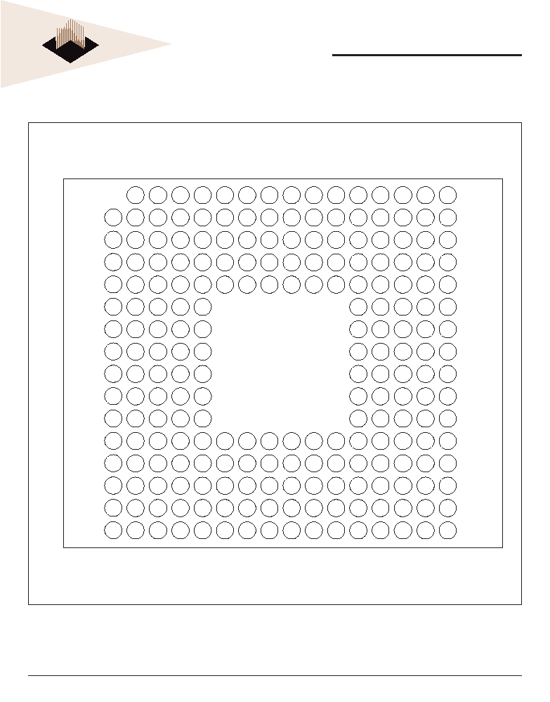
FIGURE 1 ≠ PIN CONFIGURATION
NOTE:
DNU = Do Not Use; to be left unconnected for future upgrades.
NC = Not Connected Internally.
* Pin D7 is DNU for 8M x 72 product, Pin D7 is A12 for 16M x 72 and higher densities.
Top View
3
White Electronic Designs Corporation ∑ (602) 437-1520 ∑ www.wedc.com
WEDPN8M72V-XB2X
White Electronic Designs
January 2005
Rev. 4
White Electronic Designs Corp. reserves the right to change products or specifi cations without notice.
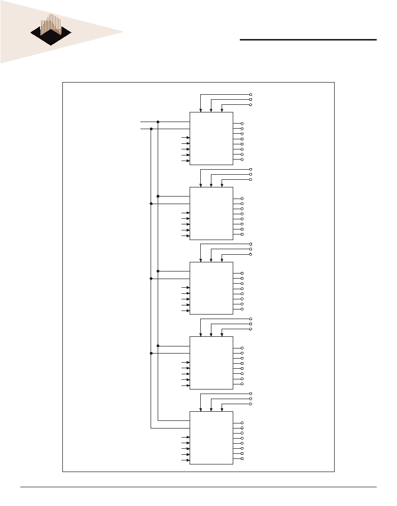
FIGURE 2 ≠ FUNCTIONAL BLOCK DIAGRAM
A
0-11
A
0-11
BA
0-1
BA
0-1
CLK
0
CLK
CAS#
DQ
0
DQ
15
CKE
0
CKE
CS
0
#
CS#
DQML
0
DQML
DQMH
0
DQMH
RAS
1
#
WE
1
#
CAS
1
#
∑
DQ
0
∑
∑
∑
∑
∑
∑
∑
∑
∑
∑
∑
DQ
15
WE#
U1
RAS#
A
0-11
BA
0-1
CLK
1
CLK
CAS#
DQ
16
DQ
31
RAS
0
#
WE
0
#
CAS
0
#
∑
DQ
0
∑
∑
∑
∑
∑
∑
∑
∑
∑
∑
∑
DQ
15
WE#
U0
RAS#
CKE
1
CKE
CS
1
#
CS#
DQML
1
DQML
DQMH
1
DQMH
RAS
2
#
WE
2
#
CAS
2
#
∑
DQ
0
∑
∑
∑
∑
∑
∑
∑
∑
∑
∑
∑
DQ
15
WE#
U2
RAS#
A
0-11
BA
0-1
CLK
2
CLK
CAS#
DQ
32
DQ
47
CKE
2
CKE
CS
2
#
CS#
DQML
2
DQML
DQMH
2
DQMH
RAS
3
#
WE
3
#
CAS
3
#
∑
DQ
0
∑
∑
∑
∑
∑
∑
∑
∑
∑
∑
∑
DQ
15
WE#
U3
RAS#
A
0-11
BA
0-1
CLK
3
CLK
CAS#
DQ
48
DQ
63
CKE
3
CKE
CS
3
#
CS#
DQML
3
DQML
DQMH
3
DQMH
RAS
4
#
WE
4
#
CAS
4
#
∑
DQ
0
∑
∑
∑
∑
∑
∑
∑
∑
∑
∑
∑
DQ
15
WE#
U4
RAS#
A
0-11
BA
0-1
CLK
4
CLK
CAS#
DQ
64
CKE
4
CKE
CS
4
#
CS#
DQML
4
DQML
DQMH
4
DQMH
DQ
79

4
White Electronic Designs Corporation ∑ (602) 437-1520 ∑ www.wedc.com
WEDPN8M72V-XB2X
White Electronic Designs
January 2005
Rev. 4
White Electronic Designs Corp. reserves the right to change products or specifi cations without notice.
The 512Mb SDRAM is designed to operate in 3.3V, low-
power memory systems. An auto refresh mode is pro vid ed,
along with a power-saving, power-down mode.
All inputs and outputs are LVTTL compatible. SDRAMs offer
sub stan tial ad vanc es in DRAM op er at ing per for mance,
in clud ing the ability to syn chro nous ly burst data at a high
data rate with automatic column-address gen er a tion, the
ability to in ter leave between in ter nal banks in order to hide
precharge time and the capability to ran dom ly change col umn
ad dress es on each clock cy cle during a burst ac cess.
FUNCTIONAL DESCRIPTION
Read and write accesses to the SDRAM are burst oriented;
accesses start at a selected location and continue for
a pro grammed number of locations in a pro grammed
se quence. Ac cess es begin with the registration of an
ACTIVE com mand which is then followed by a READ or
WRITE com mand. The address bits registered coincident
with the AC TIVE command are used to select the bank
and row to be accessed (BA0 and BA1 select the bank,
A0-11 select the row). The address bits (A0-8) reg is tered
coincident with the READ or WRITE com mand are used to
select the start ing column location for the burst access.
Prior to normal operation, the SDRAM must be initialized.
The following sections provide detailed information
cov er ing device initialization, register defi nition, command
de scrip tions and de vice operation.
INITIALIZATION
SDRAMs must be pow ered up and initialized in a pre defi ned
manner. Operational pro ce dures other than those spec i fi ed
may result in undefi ned operation. Once power is ap plied
to VDD and the clock is stable (stable clock is de fi ned as
a signal cycling within tim ing constraints specifi ed for the
clock pin), the SDRAM re quires a 100µs delay prior to
issuing any command other than a COMMAND INHIBIT
or a NOP. Starting at some point during this 100µs period
and continuing at least through the end of this period,
COMMAND INHIBIT or NOP com mands should be applied.
Once the 100µs delay has been satisfi ed with at least
one COM MAND INHIBIT or NOP command having been
ap plied, a PRECHARGE command should be applied. All
banks must be precharged, thereby placing the device in
the all banks idle state.
Once in the idle state, two AUTO REFRESH cycles must be
per formed. After the AUTO REFRESH cycles are complete,
the SDRAM is ready for Mode Register programming.
Be cause the Mode Register will power up in an unknown
state, it should be loaded prior to applying any operational
command.
REGISTER DEFINITION
MODE REGISTER
The Mode Register is used to defi ne the specifi c mode
of op er a tion of the SDRAM. This defi nition includes the
selec-tion of a burst length, a burst type, a CAS latency, an
op er at ing mode and a write burst mode, as shown in Figure
3. The Mode Register is programmed via the LOAD MODE
REG IS TER command and will retain the stored information
until it is programmed again or the device loses power.
Mode register bits M0-M2 specify the burst length, M3
spec i fi es the type of burst (sequential or in ter leaved), M4-M6
specify the CAS latency, M7 and M8 specify the op er at ing
mode, M9 spec i fi es the WRITE burst mode, and M10 and
M11 are reserved for future use.
The Mode Register must be loaded when all banks are
idle, and the controller must wait the specifi ed time before
ini ti at ing the subsequent operation. Violating either of these
requirements will result in unspecifi ed operation.
BURST LENGTH
Read and write accesses to the SDRAM are burst oriented,
with the burst length being programmable, as shown
in Fig ure 3. The burst length determines the maximum
number of column lo ca tions that can be accessed for a
given READ or WRITE command. Burst lengths of 1, 2, 4
or 8 locations are avail able for both the sequential and the
interleaved burst types, and a full-page burst is available
for the sequential type. The full-page burst is used in
conjunction with the BURST TERMINATE command to
generate arbitrary burst lengths.
Reserved states should not be used, as unknown op er a tion
or incompatibility with future versions may result.
When a READ or WRITE command is issued, a block of
col umns equal to the burst length is effectively selected. All
accesses for that burst take place within this block, mean ing
that the burst will wrap within the block if a boundary is
reached. The block is uniquely selected by A1-8 when the
burst length is set to two; by A2-8 when the burst length is set
to four; and by A3-8 when the burst length is set to eight. The
remaining (least signifi cant) address bit(s) is (are) used to
select the starting location within the block. Full-page bursts
wrap within the page if the boundary is reached.
5
White Electronic Designs Corporation ∑ (602) 437-1520 ∑ www.wedc.com
WEDPN8M72V-XB2X
White Electronic Designs
January 2005
Rev. 4
White Electronic Designs Corp. reserves the right to change products or specifi cations without notice.
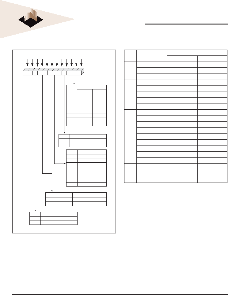
TABLE 1 ≠ BURST DEFINITION
Burst
Length
Starting Column
Address
Order of Accesses Within a Burst
Type = Sequential
Type = Interleaved
2
A0
0
0-1
0-1
1
1-0
1-0
4
A1
A0
0
0
0-1-2-3
0-1-2-3
0
1
1-2-3-0
1-0-3-2
1
0
2-3-0-1
2-3-0-1
1
1
3-0-1-2
3-2-1-0
8
A2
A1
A0
0
0
0
0-1-2-3-4-5-6-7
0-1-2-3-4-5-6-7
0
0
1
1-2-3-4-5-6-7-0
1-0-3-2-5-4-7-6
0
1
0
2-3-4-5-6-7-0-1
2-3-0-1-6-7-4-5
0
1
1
3-4-5-6-7-0-1-2
3-2-1-0-7-6-5-4
1
0
0
4-5-6-7-0-1-2-3
4-5-6-7-0-1-2-3
1
0
1
5-6-7-0-1-2-3-4
5-4-7-6-1-0-3-2
1
1
0
6-7-0-1-2-3-4-5
6-7-4-5-2-3-0-1
1
1
1
7-0-1-2-3-4-5-6
7-6-5-4-3-2-1-0
Full
Page
(y)
n = A0-9/8/7
(location 0-y)
Cn, Cn + 1, Cn + 2
Cn + 3, Cn + 4...
...Cn - 1,
Cn...
Not Supported
NOTES:
1. For full-page accesses: y = 512.
2. For a burst length of two, A1-8 select the block-of-two burst; A0 selects the starting
column within the block.
3. For a burst length of four, A2-8 select the block-of-four burst; A0-1 select the starting
column within the block.
4. For a burst length of eight, A3-8 select the block-of-eight burst; A0-2 select the starting
column within the block.
5. For a full-page burst, the full row is selected and A0-8 select the starting column.
6. Whenever a boundary of the block is reached within a given sequence above, the
following access wraps within the block.
7. For a burst length of one, A0-8 select the unique column to be accessed, and Mode
Register bit M3 is ignored.
Type = Sequential Type = Interleaved
FIGURE 3 ≠ MODE REGISTER DEFINITION
M3 = 0
1
2
4
8
Reserved
Reserved
Reserved
Full Page
M3 = 1
1
2
4
8
Reserved
Reserved
Reserved
Reserved
Operating Mode
Standard Operation
All other states reserved
0
-
0
-
Defined
-
0
1
Burst Type
Sequential
Interleaved
CAS Latency
Reserved
Reserved
2
3
Reserved
Reserved
Reserved
Reserved
Burst Length
M0
0
1
0
1
0
1
0
1
Burst Length
CAS Latency
BT
A
9
A
7
A
6
A
5
A
4
A
3
A
8
A
2
A
1
A
0
Mode Register (Mx)
Address Bus
M1
0
0
1
1
0
0
1
1
M2
0
0
0
0
1
1
1
1
M3
M4
0
1
0
1
0
1
0
1
M5
0
0
1
1
0
0
1
1
M6
0
0
0
0
1
1
1
1
M6-M0
M8
M7
Op Mode
A
10
A
11
Reserved* WB
0
1
Write Burst Mode
Programmed Burst Length
Single Location Access
M9
11 10 9
8
7
6
5
4
3
2
1
0
*Should program
M11, M10 = 0, 0 to
ensure compatibility
with future devices.