1
1
1
1
1
White Electronic Designs Corporation ∑ (602) 437-1520 ∑ www.whiteedc.com
White Electronic Designs
WEDPNF8M721V-XBX
September 2002 Rev. 3
8Mx72 Synchronous DRAM + 8Mb Flash Mixed Module
Multi-Chip Package
FEATURES
n Package:
∑ 275 Plastic Ball Grid Array (PBGA), 32mm x 25mm
n Commercial, Industrial and Military Temperature Ranges
n Weight:
∑ WEDPNF8M721V-XBX - 2.5 grams typical
SDRAM PERFORMANCE FEATURES
n Organized as 8M x 72
n High Frequency = 100, 125MHz
n Single 3.3V ±0.3V power supply
n Fully Synchronous; all signals registered on positive
edge of system clock cycle
n Internal pipelined operation; column address can be
changed every clock cycle
n Internal banks for hiding row access/precharge
n Programmable Burst length 1,2,4,8 or full page
n 4096 refresh cycles
FLASH PERFORMANCE FEATURES
n User Configurable as 1Mx8 or 512Kx16
n Access Times of 100, 120, 150ns
n 3.3 Volt for Read and Write Operations
n 1,000,000 Erase/Program Cycles
n Sector Architecture
∑ One 16KByte, two 8KBytes, one 32KByte, and fif
teen 64KBytes in byte mode
∑ One 8K word, two 4K words, one 16K word, and
fifteen 32K word sectors in word mode.
∑ Any combination of sectors can be concurrently
erased. Also suppor ts full chip erase
n Boot Code Sector Architecture (Bottom)
n Embedded Erase and Program Algorithms
n Erase Suspend/Resume
∑ Suppor ts reading data from or programing data to a
sector not being erased
BENEFITS
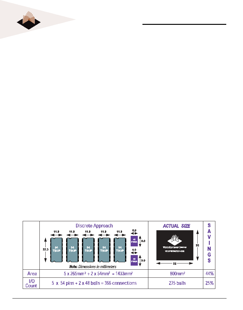
n 42% SPACE SAVINGS
n Reduced part count
n Reduced I/O count
∑ 14% I/O Reduction
n Suitable for hi-reliability applications
n SDRAM Upgradeable to 16M x 72 density (contact
factory for information)
n Flash upgradeable to 2M x 8 (or 1M x 16 or 512K x 32)
density
* This data sheet describes a product that may or may not be under
development and is subject to change or cancellation without notice.
ADVANCED*

2
2
2
2
2
White Electronic Designs Corporation ∑ Phoenix AZ ∑ (602) 437-1520
White Electronic Designs
WEDPNF8M721V-XBX
F
IG
. 1 P
IN
C
ONFIGURATION
NOTES:
1. DNU = Do Not Use
2. FD16-31, BYTE2, RY/BY2 are NC in this part, and used for flash upgraded to WEDPN8M722V-XBX (2x8M Flash).
T
OP
V
IEW
3
3
3
3
3
White Electronic Designs Corporation ∑ (602) 437-1520 ∑ www.whiteedc.com
White Electronic Designs
WEDPNF8M721V-XBX
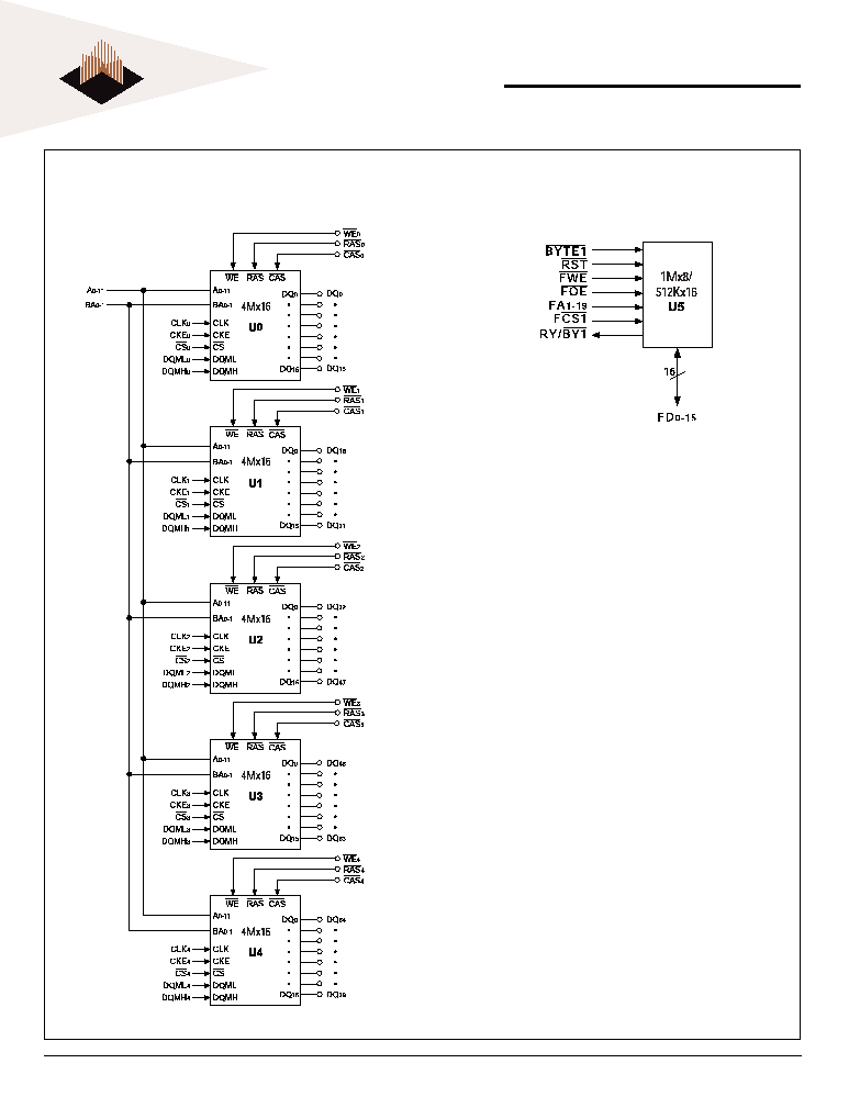
F
IG
. 2 F
UNCTIONAL
B
LOCK
D
IAGRAMS
SDRAM
FLASH
4
4
4
4
4
White Electronic Designs Corporation ∑ Phoenix AZ ∑ (602) 437-1520
White Electronic Designs
WEDPNF8M721V-XBX
Signal Name
Signal Name
Signal Name
Signal Name
Signal Name
Pin Number
Pin Number
Pin Number
Pin Number
Pin Number
V
CC
D15, E15, F8, F10, F15, G4, H4, J14, J15, J16, J17, K2, K3, K4, K5, L14, L15, L16, M5, M14, M15, N4, N5, N7, N8, N14, P4, P5, P6,
P7, P11, P12, P13, P14, R4, T15, U15, V15
GND
D4, D16, E4, F4, F7, F9, F11, F12, F13, G14, G15, H15, J2, J3, J4, J5, K14, K15, K16, K17, L4, L5, M4, N6, N9, N10, N11, N12, N13,
N15, P8, P9, P10, P15, R15, T4, U4, V4
FD0 - 15
E8, C8, E9, C9, C10, D11, C11, D12, D8, B8, D9, D10, E10, E11, E12, E13
RYBY1
H5
RST
A7
BYTE1
D13
FD16* - 31*
C12, C15, A15, B9, B11, B13, A10, A12, C13, B15, B14, B10, B12, A9, A11, A14
RYBY2*
A8
BYTE2*
A13
FA1-19
F14, F5, E7, E6, E5, D6, D5, C6, C5, C4, B6, B5, B4, A6, A5, A4, C14, D7, C7
FCS1
H14
FCS2*
E14
FWE
B7
FOE
D14
A0 - A11
V12, U13, V13, V14, T14, R13, T13, R12, T12, R11, U12, T11
BA0 - 1
U11, V11
CS0
H3
WE0
E3
CLK0
C3
CKE0
B3
RAS0
G3
CAS0
F3
DQML0
H2
DQMH0
D3
CS1
H18
WE1
J18
CLK1
B18
CKE1
A18
RAS1
G18
CAS1
F18
DQML1
E18
DQMH1
C18
CS2
T18
WE2
R18
CLK2
L18
CKE2
K18
RAS2
U18
CAS2
V18
DQML2
V17
DQMH2
M18
CS3
U3
WE3
V3
CLK3
M3
CKE3
L3
RAS3
T3
P
ACKAGE
P
INOUT
L
ISTING
*FD16-31, RY/BY2, BYTE2 are NC in this part, and used for flash upgrade to WEDPNF8M722V-XBX

5
5
5
5
5
White Electronic Designs Corporation ∑ (602) 437-1520 ∑ www.whiteedc.com
White Electronic Designs
WEDPNF8M721V-XBX
Signal Name
Signal Name
Signal Name
Signal Name
Signal Name
Pin Number
Pin Number
Pin Number
Pin Number
Pin Number
P
ACKAGE
P
INOUT
L
ISTING
(
CONTINUED
)
CAS3
R3
DQML3
U2
DQMH3
N3
CS4
T10
WE4
U9
CLK4
R9
CKE4
R10
RAS4
U10
CAS4
V10
DQML4
V9
DQMH4
T9
DQ0 - 15
E1, F1, E2, G1, F2, H1, J1, G2, A3, A2, B2, C2, B1, D2, C1, D1,
DQ16 - 31
E16, F16, G16, H16, E17, F17, G17, H17, D18, A17, B17, C17, D17, A16, B16, C16
DQ32 - 47
R17, T17, U16, V16, T16, R16, U17, P18, N16, P16, P17, M16, M17, N17, N18, L17
DQ48 - 63
R1, P2, T1, R2, P3, U1, V2, T2, M2, N2, L2, M1, P1, N1, L1, K1
DQ64 - 79
U8, U6, V5, V6, U7, U5, V7, V8, R8, R6, T8, T6, R7, R5, T7, T5
DNU
F6, G5, R14, U14, V1