
1
White Electronic Designs Corporation ∑ (602) 437-1520 ∑ www.whiteedc.com
WEDPY256K72V-XBX
DESCRIPTION
The WEDPY256K72V-XBX employs high-speed, low-power
CMOS designs that are fabricated using an advanced CMOS
process. The 16Mb Synchronous SRAMs integrate two 256K
x 36 SRAMs into a single PBGA package to provide 256K x
72 configuration. All synchronous inputs are controlled by
a positive-edge-triggered single-clock input (CLK). The syn-
chronous inputs include all addresses, all data inputs, and
active LOW chip selects (CS). Asynchronous inputs in-
clude the output enable (OE1/OE2), clock (CLK).
* This data sheet describes a product that is not fully qualified or characterized
and is subject to change without notice.
November 2003 Rev. 6
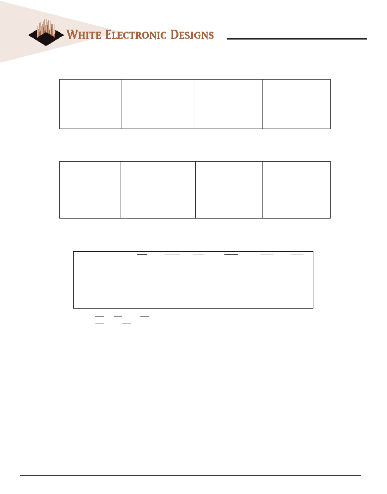
256Kx72 Synchronous Pipeline SRAM
FEATURES
!
Fast clock speed: 100, 133, 150, 166 and 200** MHz
!
Fast access time: 5.0, 4.0, 3.8, 3.5, 3.1ns
!
+3.3V power supply (VDD)
!
+2.5V output buffer supply (VDDQ)
!
Single-cycle deselect
!
Common data inputs and data outputs
!
Clock-controlled and registered addresses, data I/Os
and control signals
!
SNOOZE MODE for reduced-power standby
!
Individual BYTE WRITE control and GLOBAL WRITE
!
Six chip enables for simple depth expansion and ad-
dress pipeline
!
Internally self-timed WRITE cycle
!
Burst control (interleaved or linear burst)
!
Packaging:
!
159-bump PBGA package, 14mm x 22mm
!
Commercial, industrial, and military temperature ranges
!
User configurable as 512K x 36, or 1M x 18
!
Upgradable to 512K x 72 SSRAM
(contact factory for information)
**200 MHz for commercial and industrial temperature only.
FIG. 1
BLOCK DIAGRAM
SA
0-17
ADSC
ADSP
ADV
BWa
BWb
BWc
BWd
BWE
CS1
1
CS2
1
CS2
1
CLK
GW
MODE
OE
1
ZZ
A
0-17
ADSC
ADSP
ADV
BWa
BWb
BWc
BWd
WE
CS
1
CS
2
CS
2
CLK
GW
MODE
OE
ZZ
256Kx36
SSRAM
IC1
DQ
0-35
DQ
0-35
DQ
36-71
A
0-17
ADSC
ADSP
ADV
BWa
BWb
BWc
BWd
WE
CS
1
CS
2
CS
2
CLK
GW
MODE
OE
ZZ
256Kx36
SSRAM
IC2
BWe
BWf
BWg
BWh
CS1
1
CS2
2
CS2
2
OE
2
Preliminary*

2
White Electronic Designs Corporation ∑ Phoenix AZ ∑ (602) 437-1520
WEDPY256K72V-XBX
1
1
1
1
1
2
2
2
2
2
3
3
3
3
3
4
4
4
4
4
5
5
5
5
5
6
6
6
6
6
7
7
7
7
7
8
8
8
8
8
9
9
9
9
9
1 0
1 0
1 0
1 0
1 0
A
A
A
A
A
--
D Q 1 6
D Q 1 4
D Q 1 2
D Q 1 0
ZZ
D Q 6
D Q 4
D Q ÿ
D Q 8
B
B
B
B
B
ADV
DQ17
DQ15
DQ11
DQ9
DQ7
DQ5
DQ3
DQ1
SA13
C
C
C
C
C
O E 1
ADSP
GW
D Q 1 3
DNU
GND
D Q 2 9
D Q 2
SA12
SA10
D
D
D
D
D
CS2
1
CLK
BWa
GND
GND
V D D
V D D Q
SA11
SA9
SA6
E
E
E
E
E
BW
C
BWb
BWd
GND
V D D
GND
GND
SA8
SA7
SAÿ
F
F
F
F
F
CS2
1
D Q 1 8
D Q 2 2
V D D
V D D Q
GND
V D D
D Q 3 0
D Q 3 4
SA1
G
G
G
G
G
CS1
1
D Q 1 9
D Q 2 3
GND
V D D
V D D Q
GND
D Q 3 1
D Q 3 3
SA5
H
H
H
H
H
D Q 2 6
D Q 2 0
D Q 2 4
V D D Q
V D D Q
V D D
V D D
D Q 2 8
D Q 3 2
D Q 3 5
J
J
J
J
J
SA17
D Q 2 1
D Q 2 5
V D D
V D D
V D D Q
V D D Q
D Q 2 7
D Q 3 9
D Q 3 7
K
K
K
K
K
SA16
D Q 5 2
D Q 4 9
GND
V D D Q
V D D
GND
D Q 4 0
D Q 3 8
D Q 3 6
L
L
L
L
L
SA14
D Q 5 1
D Q 5 0
V D D
GND
V D D Q
V D D
D Q 4 2
D Q 4 1
D Q 4 4
M
M
M
M
M
SA15
D Q 5 3
D Q 4 8
GND
GND
V D D
GND
D Q 4 3
SA3
DNU
N
N
N
N
N
O E 2
ADSC
D Q 4 7
V D D Q
V D D
GND
GND
MODE
SA2
SA4
P
P
P
P
P
BWE
CS2
2
D Q 4 6
D Q 4 5
GND
DNU
D Q 5 9
D Q 6 4
D Q 6 6
D Q 7 0
R
R
R
R
R
BWh
BWg
BWf
BWe
D Q 5 6
D Q 6 0
D Q 6 1
D Q 6 5
D Q 6 9
D Q 7 1
T
T
T
T
T
CS1
2
CS2
2
D Q 6 2
D Q 5 4
D Q 5 5
D Q 5 7
D Q 5 8
D Q 6 3
D Q 6 7
D Q 6 8
DNU = DO NOT USE. Reserved for future upgrades.
P
IN
C
ONFIGURATION
(T
OP
V
IEW
)
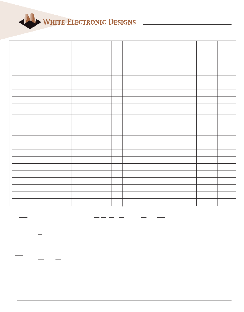
3
White Electronic Designs Corporation ∑ (602) 437-1520 ∑ www.whiteedc.com
WEDPY256K72V-XBX
First Address (External)
Second Address (Internal)
Third Address (Internal)
Fourth Address (Internal)
X...X00
X...X01
X...X10
X...X11
X...X01
X...X00
X...X11
X...X10
X...X10
X...X11
X...X00
X...X01
X...X11
X...X10
X...X01
X...X00
I
NTERLEAVED
B
URST
A
DDRESS
T
ABLE
(M
ODE
= NC
OR
H
IGH
)
L
INEAR
B
URST
A
DDRESS
T
ABLE
(M
ODE
= L
OW
)
P
ARTIAL
T
RUTH
T
ABLE
FOR
W
RITE
C
OMMANDS
(
X
36)
NOTE:
1. Using BWE and BWa through BWd, any one or more bytes may be written.
2. Insert BWe through BWh for DQ36-71 control.
Function
GW
BWE
BWa
BWb
BWc
BWd
READ
H
H
X
X
X
X
READ
H
L
H
H
H
H
WRITE Byte "a"
H
L
L
H
H
H
WRITE All Bytes
H
L
L
L
L
L
WRITE All Bytes
L
X
X
X
X
X
First Address (External)
Second Address (Internal)
Third Address (Internal)
Fourth Address (Internal)
X...X00
X...X01
X...X10
X...X11
X...X01
X...X10
X...X11
X...X00
X...X10
X...X11
X...X00
X...X01
X...X11
X...X00
X...X01
X...X10
4
White Electronic Designs Corporation ∑ Phoenix AZ ∑ (602) 437-1520
WEDPY256K72V-XBX
NOTE:
1. X means "Don't Care." means active LOW. H means logic HIGH. L means logic LOW.
2. For WRITE, L means any one or more byte write enable signals (BWa, BWb, BWc, or WE) are LOW or GW is LOW. WRITE = H for
all BWx, BWE, GW High.
3. BWa enables WRITEs to DQ0-8. BWb enables WRITEs to DQ9-17. BWc enables WRITEs to DQ18-26. BWd enables WRITE to
DQ27-35.
4. All inputs excepts OE and ZZ must meet setup and hold times around the rising edge (LOW to HIGH) of CLK.
5. Wait states are inserted by suspending bursts.
6. For a WRITE operation following a READ operation, OE must be HIGH before the input data setup time and held HIGH throughout
the input data hold time.
7. This device contains circuitry that will ensure the outputs will be held in High-Z during power-up.
8. ADSP LOW always initiates an internal READ at the L-H edge of CLK. A WRITE is performed by setting one or more byte write
enable signals and BWE LOW or GW LOW for the subsequent L-H edge of CLK. Refer to WRITE timing diagram for clarification.
T
RUTH
T
ABLE
Operation
Address Used
CS1
CS2 CS2 ZZ
ADSP
ADSC ADV WRITE OE
CLK
DQ
Deselected Cycle, Power-Down
None
H
X
X
L
X
L
X
X
X
L-H
HIGH Z
Deselected Cycle, Power-Down
None
L
X
L
L
L
X
X
X
X
L-H
HIGH Z
Deselected Cycle, Power-Down
None
L
H
X
L
L
X
X
X
X
L-H
HIGH Z
Deselected Cycle, Power-Down
None
L
X
L
L
H
L
X
X
X
L-H
HIGH Z
Deselected Cycle, Power-Down
None
L
H
X
L
H
L
X
X
X
L-H
HIGH Z
SNOOZE MODE, Power-Down
None
X
X
X
H
X
X
X
X
X
X
HIGH Z
READ Cycle, Begin Burst
External
L
L
H
L
L
X
X
X
L
L-H
Q
READ Cycle, Begin Burst
External
L
L
H
L
L
X
X
X
H
L-H
HIGH Z
WRITE Cycle, Begin Burst
External
L
L
H
L
H
L
X
L
X
L-H
D
READ Cycle, Begin Burst
External
L
L
H
L
H
L
X
H
L
L-H
Q
READ Cycle, Begin Burst
External
L
L
H
L
H
L
X
H
H
L-H
HIGH Z
READ Cycle, Continue Burst
Next
X
X
X
L
H
H
L
H
L
L-H
Q
READ Cycle, Continue Burst
Next
X
X
X
L
H
H
L
H
H
L-H
HIGH Z
READ Cycle, Continue Burst
Next
H
X
X
L
X
H
L
H
L
L-H
Q
READ Cycle, Continue Burst
Next
H
X
X
L
X
H
L
H
H
L-H
HIGH Z
WRITE Cycle, Continue Burst
Next
X
X
X
L
H
H
L
L
X
L-H
D
WRITE Cycle, Continue Burst
Next
H
X
X
L
X
H
L
L
X
L-H
D
READ Cycle, Suspend Burst
Current
X
X
X
L
H
H
H
H
L
L-H
Q
READ Cycle, Suspend Burst
Current
X
X
X
L
H
H
H
H
H
L-H
HIGH Z
READ Cycle, Suspend Burst
Current
H
X
X
L
X
H
H
H
L
H
Q
READ Cycle, Suspend Burst
Current
H
X
X
L
X
H
H
H
H
L-H
HIGH Z
WRITE Cycle, Suspend Burst
Current
X
X
X
L
H
H
H
L
X
L-H
D
WRITE Cycle, Suspend Burst
Current
H
X
X
L
X
H
H
L
X
L-H
D

5
White Electronic Designs Corporation ∑ (602) 437-1520 ∑ www.whiteedc.com
WEDPY256K72V-XBX
Description
Symbol
Conditions
Min
Max
Units
Notes
Input High (Logic 1)Voltage
V
IH
Inputs
1.7
V
DD
+0.3
V
1
V
IHQ
Data (DQ)
1.7
V
DDQ
+0.3
V
1
Input Low (Logic 0) Voltage
V
IL
-0.3
0.7
V
1
Input Leakage Current
I
LI
0V
V
IN
V
DD
-2.0
2.0
µA
2
Ouptut Leakage Current
I
LO
Outputs disabled, 0V
V
IN
V
DDQ
(DQ
X
)
-1.0
1.0
µA
Output High Voltage
V
OH
I
OH
= -1.0mA
2.0
--
V
1
Output Low Voltage
V
OL
I
OL
= 1.0mA
--
0.4
V
1
Supply Voltage
V
DD
3.135
3.6
V
1
Output Buffer Supply
V
DDQ
2.375
2.9
V
1
Description
Symbol
Max
Units
Notes
Control Input Capacitance
C
I
6
pF
1
Common Control Input Capacitance (2)
C
IC
15
pF
1
Input/Output Capacitance (DQ)
C
O
10
pF
1
Address Capacitance (SA)
Cs
A
15
pF
1
Clock Capacitance (CLK)
C
CK
12
pF
1
BGA C
APACITANCE
(T
A
= +25∞C, F = 1MH
Z
)
DC C
HARACTERISTICS
-55∞C
TA
+125∞C
E
LECTRICAL
C
HARACTERISTICS
A
ND
O
PERATING
CONDITIONS
-55∞C
TA
+125∞C
A
BSOLUTE
M
AXIMUM
R
ATINGS
*
Voltage on V
DD
Supply relative to V
SS
-0.5V to +4.6V
Voltage on V
DDQ
Supply relative to V
SS
-0.5V to +4.6V
VIN (DQx)
-0.5V to V
DDQ
+0.5V
VIN (Inputs)
-0.5V to V
DD
+0.5V
Storage Temperature (BGA)
-55∞C to +150∞C
Shor t Circuit Output Current
100 mA
*Stress greater than those listed under "Absolute Maximum Ratings" may cause
permanent damage to the device. This is a stress rating only, and functional
operation of the device at these or any other conditions greater than those
indicated in the operational sections of this specification is not implied. Exposure
to absolute maximum rating conditions for extended periods may affect reliability.
NOTES:
1. IDD is specified with no output current and increases with faster cycle times. IDD increases with faster cycle times and greater output loading.
2. "Device deselected" means device is in power-down mode as defined in the truth table. "Device selected" means device is active (not in power-down
mode).
NOTES:
1. All voltages referenced to Vss (GND).
Description
Conditions
100 MHz
133 MHz 150 MHz 160 MHz 200 MHz Units
Notes
Power Supply
IDD
Device selected; All inputs
VIL or
VIH;
Current: Operating
Cycle time
tKC MIN; VDD = MAX; Outputs open
600
750
950
950
1050
mA
1.2
CMOS Standby
ISB2
Device deselected; VDD = MAX; All inputs
Vss + 0.2
20
20
20
20
20
mA
2
Clock Running
ISB4
Device deselected; VDD = MAX; All inputs
Vss +
0.2 or
VDD -0.2; Cycle time
tKC MIN; ADSC,
170
180
220
220
240
mA
2
ADSP, GW, BWx, ADV,
VIH
NOTES:
1. This parameter is guaranteed by design but not tested.
2. Common Inputs = zz, ADV, ADSP, GW, ADSC, MODE, BWE
BGA T
HERMAL
R
ESISTANCE
Description
Description
Description
Description
Description
Symbol
Symbol
Symbol
Symbol
Symbol Max
Max
Max
Max
Max
Units
Units
Units
Units
Units
Notes
Notes
Notes
Notes
Notes
Junction to Ambient
Theta JA 30.5
0
C/W
1
(No Airflow)
Junction to Ball
Theta JB 17.3
0
C/W
1
Junction to Case (Top)
Theta JC
9.8
0
C/W
1
NOTE 1: Refer to BGA Thermal Resistance Correlation
application note at www.whiteedc.com in the application
notes section for modeling conditions.
6
White Electronic Designs Corporation ∑ Phoenix AZ ∑ (602) 437-1520
WEDPY256K72V-XBX
NOTES:
1. Test conditions as specified with the output loading as shown in test conditions unless otherwise noted.
2. This parameter is measured with output load as shown in test conditions.
3. This parameter is not tested.
4. Transition is measured ±500mV from steady state voltage.
5. OE is a "Don't Care" when a byte write enable is sampled LOW.
6. Measured at HIGH above VIH and LOW below VIL
7. This is a synchronous device. All addresses must meet the specified setup and hold times for all rising edges of CLK. All other synchronous inputs must meet the setup
and hold times with stable logic levels for all rising edges of clock (CLK) when the chip is enabled. Chip enable must be valid at each rising edge of CLK to remain
enabled.
AC C
HARACTERISTICS
-55∞C
TA
+125∞C
O
UTPUT
L
OADS
AC Output Load Equivalent
Parameter
2.5V I/O
Unit
Input Pulse Levels
Vss to 2.5
V
Input Rise and Fall Times
1
ns
Input Timing Reference Levels
1.25
V
Output Timing Reference Levels
1.25
V
Output Load
See figures, at left
* Commercial and industrial temperatures only.
Symbol 100MHz 133MHz 150MHz 166MHz 200MHz*
Parameter
Min.
Max
Min
Max
Min
Max
Min
Max
Min
Max
Units
Clock
Clock Cycle Time
tkc
10
7.5
7.0
6.0
5.0
ns
Clock Frequency
tkf
100
133
150
166
200
MHz
Clock HIGH Time (6)
tkh
3.0
2.5
2.5
2.3
2.0
ns
Clock LOW Time (6)
tkl
3.0
2.5
2.5
2.3
2.0
ns
Output Times
Clock to output valid
tkq
5.0
4.0
3.8
3.5
3.1
ns
Clock to output invalid (2)
tkqx
1.5
1.5
1.5
15
1.0
ns
Clock to output on Low-Z (2,3,4)
tkqlz
1.5
0
0
0
0
ns
Clock to output in High-Z (2,3,4)
tkqhz
5.0
4.2
4.0
3.5
3.1
ns
OE to output valid (5)
toeq
5.0
4.2
4.0
3.5
3.1
ns
OE to output in Low-Z (2,3,4)
toelz
0
0
0
0
0
ns
OE to output in High Z (2,3,4)
toehz
4.5
4.2
4.0
3.5
3.0
ns
Setup Time
Address (6,7)
tas
2.0
1.5
1.5
1.5
1.5
ns
Write Enable (WE) (7)
tws
2.0
1.5
1.5
1.5
1.5
ns
Address status, (ADSC, ADSP) (7)
tadss
2.0
1.5
1.5
1.5
1.5
ns
Address advance (ADV) (7)
taas
2.0
1.5
1.5
1.5
1.5
ns
Data-in (6,7)
tds
2.0
1.5
1.5
1.5
1.5
ns
Chip enable (CE) (7)
tces
2.0
1.5
1.5
1.5
1.5
ns
Hold Times
Address (7) (7)
tah
0.5
0.5
0.5
0.5
0.5
ns
Address status (ADSC, ADSP) (7)
tadsh
0.5
0.5
0.5
0.5
0.5
ns
Address advance (ADV) (7)
taah
0.5
0.5
0.5
0.5
0.5
ns
Write Enable (WE) (7)
twh
0.5
0.5
0.5
0.5
0.5
ns
Data-in (6,7)
tdh
0.5
0.5
0.5
0.5
0.5
ns
Chip Enable (CS) (7)
tceh
0.5
0.5
0.5
0.5
0.5
ns
AC T
EST
C
ONDITIONS
7
White Electronic Designs Corporation ∑ (602) 437-1520 ∑ www.whiteedc.com
WEDPY256K72V-XBX
Description
Conditions Symbol
Min
Max
Units
Notes
Current during SNOOZE MODE
ZZ
V
IH
I
SB2Z
20
mA
ZZ active to input ignored
tZZ
2 (tKC)
ns
1
ZZ inactive to input sampled
tRZZ
2(
t
KC)
ns
1
ZZ active to snooze current
tZZI
2 (tKC)
ns
1
ZZ inactive to exit snooze current
tRZZI
0
ns
1
SNOOZE MODE
SNOOZE MODE is a low-current, "power-down" mode in
which the device is deselected and current is reduced to
ISB2Z. The duration of SNOOZE MODE is dictated by the
length of time ZZ is in a HIGH state. After the device enters
SNOOZE MODE, all inputs except ZZ become gated in-
puts and a ignored.
ZZ is an asynchronous, active HIGH input that causes
the device to enter SNOOZE MODE. When ZZ becomes
a logic HIGH, ISB2Z is guaranteed after the setup time tzz is
met. Any READ or WRITE operation pending when the de-
vice enters SNOOZE MODE is not guaranteed to complete
successfully. Therefore, SNOOZE MODE must not be initi-
ated until valid pending operations are completed.
S
NOOZE
M
ODE
E
LECTRICAL
C
HARACTERISTICS
S
NOOZE
M
ODE
W
AVEFORM
NOTES:
1. This parameter is sampled.
ZZ
I
SUPPLY
CLOCK
ALL INPUTS
(except ZZ)
Output (Q)
t
ZZ
t
ZZI
t
RZZ
t
RZZI
HIGH-Z
DESELECT or READ Only
I
ISB2Z
DON'T CARE
Deselect or Read Only
Normal
Operation Cycle

8
White Electronic Designs Corporation ∑ Phoenix AZ ∑ (602) 437-1520
WEDPY256K72V-XBX
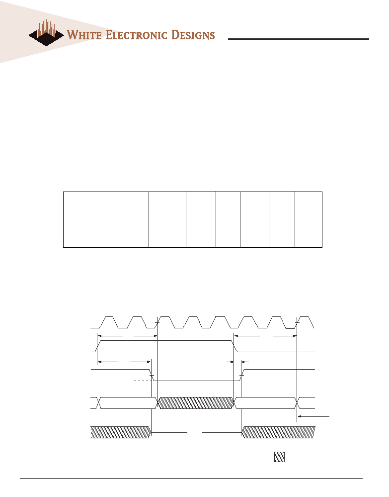
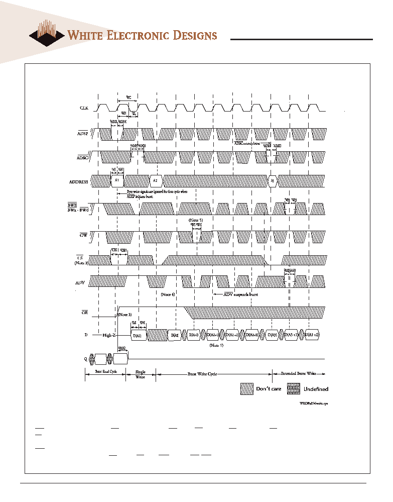
FIG. 2: READ TIMING
3
NOTES:
1. DQ (A2) refers to output from address A2. DQ (A2+ 1) refers to output from the next internal burst address following A2.
2. CS2 and CS2 have timing identical to CS1. On this diagram. When CS1 is LOW, CS2 is LOW and CS2 is HIGH. When CS1 is HIGH, CS2 is HIGH and CS2 is LOW.
3. Timing is shown assuming that the device was not enabled before entering into this sequence. OE does not cause Q to be driven until after the following
clock rising edge.
4. Outputs are disabled within two clock cycles after deselect.
9
White Electronic Designs Corporation ∑ (602) 437-1520 ∑ www.whiteedc.com
WEDPY256K72V-XBX
NOTES:
1. D(A2) refers to input for address A2. D(A2 +1) refers to input for the next internal burst address following A2.
2. CS2 and CS2 have timing identical to CS1. On this diagram, when CS1 is LOW, CS2 is LOW and CS2 is HIGH. When CS1 is HIGH, CS2 is HIGH and CS2 is LOW.
3. OE msut be HIGH before the input data setup and held HIGH throughout the data hold time. This prevents input/output data contentinon for th etime period
prior to the byte write enable inputs being sampled.
4. ADV must be HIGH to permit a WRITE to the loaded address.
5. Full-width WRITE can be initiated by GW LOW; or GW HIGH, BWE LOW and BWa-BWd LOW.
FIG. 3: WRITE TIMING
10
White Electronic Designs Corporation ∑ Phoenix AZ ∑ (602) 437-1520
WEDPY256K72V-XBX
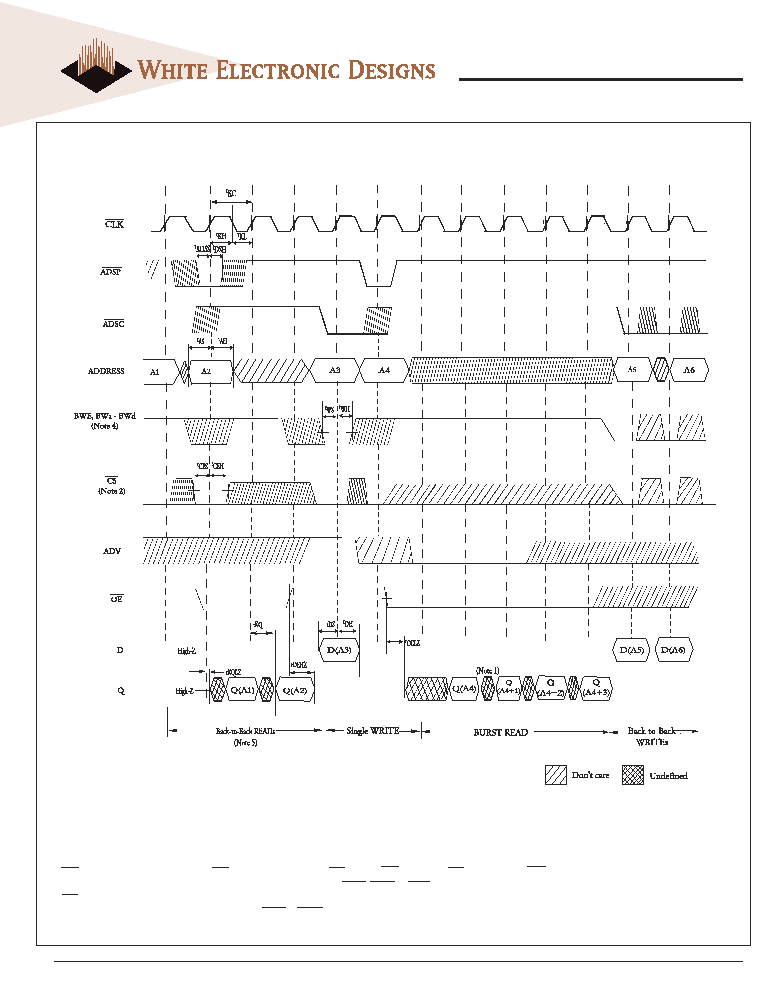
FIG. 5: READ/WRITE TIMING
3
NOTES:
1. Q(A4) refers to output from addrss A4. Q(A4 + 1) refers to output from the next internal burst address to following A4.
2. CS2 and CS2 have timing identical to CS1. On this diagram, when CS1 is LOW, CS2 is LOW and CS2 is HIGH. When CS1 is HIGH, CS2 is HIGH and CS2 is LOW.
3. The data bus (Q) remains in High-Z following a WRITE cycle unless an ADSP, ADSC, or ADV cycle is performed.
4. GW is HIGH.
5. Back-to back READs may be controlled by either ADSP or ADSC.

11
White Electronic Designs Corporation ∑ (602) 437-1520 ∑ www.whiteedc.com
WEDPY256K72V-XBX
PACKAGE DIMENSION: 159 BUMP PBGA
ALL LINEAR DIMENSIONS ARE MILLIMETERS AND PARENTHETICALLY IN INCHES
ORDERING INFORMATION
DEVICE GRADE:
M = Military
-55∞C to +125∞C
I = Industrial
-40∞C to +85∞C
C = Commercial
0∞C to +70∞C
PACKAGE:
B = 159 Plastic Ball Grid Array (PBGA)
FREQUENCY (MHz)
100 = 100MHz
133 = 133MHz
150 = 150MHz
166 = 166MHz
200 = 200MHZ
3.3V Power Supply
CONFIGURATION, 256k x 72
SSRAM, Pipeline Burst
PLASTIC
WHITE ELECTRONIC DESIGNS CORP.
X
X
V -
256K72
WED P Y
2.03 (0.080) MAX
0.61 (0.024) NOM
14.1 (0.555) MAX
11.43 (0.450) NOM
22.1 (0.870) MAX
19.05 (0.750) NOM
1.27 (0.050) NOM
1.27 (0.050) NOM
159x
0.762 (0.030) NOM
BOTTOM VIEW
B

12
White Electronic Designs Corporation ∑ Phoenix AZ ∑ (602) 437-1520
WEDPY256K72V-XBX
Document Title
256K x 72 Synchronous SRAM
Revision History
Rev #
History
Release Date
Status
Rev 0
Initial Release
July 2001
Advanced
Rev 1
Changes (Pg. 1, 5)
1.1 Add speed grades (100MHz-200MHz) to DC Characteristics Table
Rev 2
Change (Pg. 1)
January 2002
Preliminary
1.1 Change product status from Advanced to Preliminary.
Rev 3
Change (Pg. 1, 11)
September 2002
Preliminary
1.1 Change Package Dimension title from Top View to Bottom View
Rev 4
Changes (Pg. 1, 5)
November 2002
Preliminary
1.1 BGA Capacitance: Change C
I
from 10pF to 6pF
1.2 Change C
IP
to C
IC
, capacitance from 20pF to 15pF
1.3 Change C
CK
from 20pF to 12pF
1.4 Change C
O
from 12pF to 10pF
1.5 Change C
SA
from 20pF to 15pF
1.6 Add Note 2: Control Inputs = zz, ADV#, ADSP#, GW#, ADSC#, MODE#, BWE#.
Rev 5
Changes (Pg. 1, 5, 7, 12)
May 2003
Preliminary
1.1 Add Thermal Resistance Table
1.2 Correct formatting on page 7
Rev 6
Changes (Pg. 1, 11, 12)
November 2003
Preliminary
1.1 Change mechanical drawing to new style