
1
White Electronic Designs Corporation ∑ (602) 437-1520 ∑ www.wedc.com
White Electronic Designs
WEDPY256K72V-XBX
August 2004
Rev. 7
DESCRIPTION
The WEDPY256K72V-XBX employs high-speed, low-
power CMOS designs that are fabricated using an
advanced CMOS process. The 16Mb Synchronous
SRAMs integrate two 256K x 36 SRAMs into a single
PBGA package to provide 256K x 72 confi guration. All
synchronous inputs are controlled by a positive-edge-
triggered single-clock input (CLK). The synchronous inputs
include all addresses, all data inputs, and active LOW chip
selects (CS#). Asynchronous inputs include the output
enable (OE1#/OE2#), clock (CLK).
* This product is subject to change without notice.
256Kx72 Synchronous Pipeline SRAM
FEATURES
Fast clock speed: 100, 133, 150, 166
and 200** MHz
Fast access time: 5.0, 4.0, 3.8, 3.5, 3.1ns
+3.3V power supply (V
CC
)
+2.5V output buffer supply (V
CCQ
)
Single-cycle deselect
Common data inputs and data outputs
Clock-controlled and registered addresses, data
I/Os and control signals
SNOOZE MODE for reduced-power standby
Individual BYTE WRITE control and GLOBAL
WRITE
Six chip enables for simple depth expansion and
address pipeline
Internally self-timed WRITE cycle
Burst control (interleaved or linear burst)
Packaging:
159-bump PBGA package, 14mm x 22mm
Commercial, industrial, and military temperature
ranges
User confi gurable as 512K x 36, or 1M x 18
**200 MHz for commercial and industrial temperature only.
FIGURE 1 ≠ BLOCK DIAGRAM
SA
0-17
ADSC#
ADSP#
ADV#
BWa#
BWb#
BWc#
BWd#
BWE#
CS1
1
#
CS2
1
#
CS2
1
CLK
GW#
MODE
OE
1#
ZZ
A
0-17
ADSC#
ADSP#
ADV#
BWa#
BWb#
BWc#
BWd#
WE#
CS
1
#
CS
2
#
CS
2
CLK
GW#
MODE
OE#
ZZ
A
0-17
ADSC#
ADSP#
ADV#
BWa#
BWb#
BWc#
BWd#
WE#
CS
1
#
CS
2
#
CS
2
CLK
GW#
MODE
OE#
ZZ
256Kx36
SSRAM
IC1
DQ
0-35
DQ
0-35
DQ
36-71
256Kx36
SSRAM
IC2
BWe#
BWf#
BWg#
BWh#
CS1
1
#
CS2
2
#
CS2
2
OE
2
#
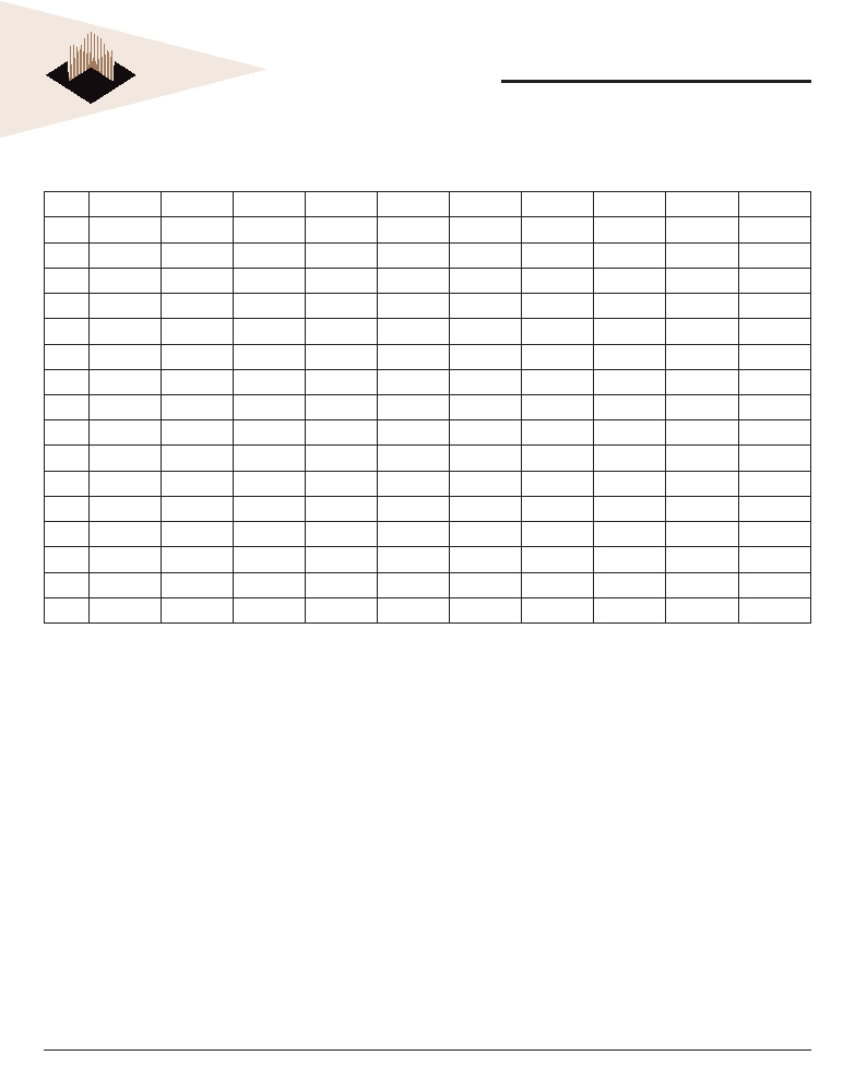
2
White Electronic Designs Corporation ∑ (602) 437-1520 ∑ www.wedc.com
White Electronic Designs
WEDPY256K72V-XBX
August 2004
Rev. 7
PIN CONFIGURATION
(Top View)
1
2
3
4
5
6
7
8
9
10
A
--
DQ16
DQ14
DQ12
DQ10
ZZ
DQ6
DQ4
DQÿ
DQ8
B
ADV#
DQ17
DQ15
DQ11
DQ9
DQ7
DQ5
DQ3
DQ1
SA13
C
OE1#
ADSP#
GW#
DQ13
DNU
GND
DQ29
DQ2
SA12
SA10
D
CS21#
CLK
BWa#
GND
GND
V
CC
V
CCQ
SA11
SA9
SA6
E
BWc#
BWb#
BWd#
GND
V
CC
GND
GND
SA8
SA7
SAÿ
F
CS2
1
DQ18
DQ22
V
CC
V
CCQ
GND
V
CC
DQ30
DQ34
SA1
G
CS1
1
#
DQ19
DQ23
GND
V
CC
V
CCQ
GND
DQ31
DQ33
SA5
H
DQ26
DQ20
DQ24
V
CCQ
V
CCQ
V
CC
V
CC
DQ28
DQ32
DQ35
J
SA17
DQ21
DQ25
V
CC
V
CC
V
CCQ
V
CCQ
DQ27
DQ39
DQ37
K
SA16
DQ52
DQ49
GND
V
CCQ
V
CC
GND
DQ40
DQ38
DQ36
L
SA14
DQ51
DQ50
V
CC
GND
V
CCQ
V
CC
DQ42
DQ41
DQ44
M
SA15
DQ53
DQ48
GND
GND
V
CC
GND
DQ43
SA3
DNU
N
OE2#
ADSC#
DQ47
V
CCQ
V
CC
GND
GND
MODE
SA2
SA4
P
BWE#
CS2
2
#
DQ46
DQ45
GND
DNU
DQ59
DQ64
DQ66
DQ70
R
BWh#
BWg#
BWf#
BWe#
DQ56
DQ60
DQ61
DQ65
DQ69
DQ71
T
CS1
2
#
CS2
2
DQ62
DQ54
DQ55
DQ57
DQ58
DQ63
DQ67
DQ68
DNU = DO NOT USE. RESERVED FOR FUTURE UPGRADES.
3
White Electronic Designs Corporation ∑ (602) 437-1520 ∑ www.wedc.com
White Electronic Designs
WEDPY256K72V-XBX
August 2004
Rev. 7
INTERLEAVED BURST ADDRESS TABLE (MODE = NC OR HIGH)
First Address (External)
Second Address (Internal)
Third Address (Internal)
Fourth Address (Internal)
X...X00
X...X01
X...X10
X...X11
X...X01 X...X00
X...X11
X...X10
X...X10 X...X11
X...X00
X...X01
X...X11 X...X10
X...X01
X...X00
LINEAR BURST ADDRESS TABLE (MODE = LOW)
First Address (External)
Second Address (Internal)
Third Address (Internal)
Fourth Address (Internal)
X...X00
X...X01
X...X10
X...X11
X...X01
X...X10
X...X11
X...X00
X...X10
X...X11
X...X00
X...X01
X...X11
X...X00
X...X01
X...X10
PARTIAL TRUTH TABLE FOR WRITE COMMANDS (X36)
Function GW#
BWE#
BWa#
BWb#
BWc#
BWd#
READ
H
H
X
X
X X
READ
H
L H H
H
H
WRITE Byte "a"
H
L
L
H
H
H
WRITE All Bytes
H
L
L
L
L
L
WRITE All Bytes
L
X
X
X
X
X
NOTE:
1. Using BWE# and BWa# through BWd#, any one or more bytes may be written.
2. Insert BWe# through BWh# for DQ36-71 control.

4
White Electronic Designs Corporation ∑ (602) 437-1520 ∑ www.wedc.com
White Electronic Designs
WEDPY256K72V-XBX
August 2004
Rev. 7
TRUTH TABLE
Operation
Address Used
CS1
CS2
CS2
ZZ
ADSP
ADSC
ADV
WRITE
OE
CLK
DQ
Deselected Cycle, Power-Down
None
H
X
X
L
X
L
X
X
X
L-H
HIGH Z
Deselected Cycle, Power-Down
None
L
X
L
L
L
X
X
X
X
L-H
HIGH Z
Deselected Cycle, Power-Down
None
L
H
X
L
L
X
X
X
X
L-H
HIGH Z
Deselected Cycle, Power-Down
None
L
X
L
L
H
L
X
X
X
L-H
HIGH Z
Deselected Cycle, Power-Down
None
L
H
X
L
H
L
X
X
X
L-H
HIGH Z
SNOOZE MODE, Power-Down
None
X
X
X
H
X
X
X
X
X
X
HIGH Z
READ Cycle, Begin Burst
External
L
L
H
L
L
X
X
X
L
L-H
Q
READ Cycle, Begin Burst
External
L
L
H
L
L
X
X
X
H
L-H
HIGH Z
WRITE Cycle, Begin Burst
External
L
L
H
L
H
L
X
L
X
L-H
D
READ Cycle, Begin Burst
External
L
L
H
L
H
L
X
H
L
L-H
Q
READ Cycle, Begin Burst
External
L
L
H
L
H
L
X
H
H
L-H
HIGH Z
READ Cycle, Continue Burst
Next
X
X
X
L
H
H
L
H
L
L-H
Q
READ Cycle, Continue Burst
Next
X
X
X
L
H
H
L
H
H
L-H
HIGH Z
READ Cycle, Continue Burst
Next
H
X
X
L
X
H
L
H
L
L-H
Q
READ Cycle, Continue Burst
Next
H
X
X
L
X
H
L
H
H
L-H
HIGH Z
WRITE Cycle, Continue Burst
Next
X
X
X
L
H
H
L
L
X
L-H
D
WRITE Cycle, Continue Burst
Next
H
X
X
L
X
H
L
L
X
L-H
D
READ Cycle, Suspend Burst
Current
X
X
X
L
H
H
H
H
L
L-H
Q
READ Cycle, Suspend Burst
Current
X
X
X
L
H
H
H
H
H
L-H
HIGH Z
READ Cycle, Suspend Burst
Current
H
X
X
L
X
H
H
H
L
H
Q
READ Cycle, Suspend Burst
Current
H
X
X
L
X
H
H
H
H
L-H
HIGH Z
WRITE Cycle, Suspend Burst
Current
X
X
X
L
H
H
H
L
X
L-H
D
WRITE Cycle, Suspend Burst
Current
H
X
X
L
X
H
H
L
X
L-H
D
NOTE:
1. X means "Don't Care." # means active LOW. H means logic HIGH. L means logic LOW.
2. For WRITE#, L means any one or more byte write enable signals (BWa#, BWb#, BWc#, or WE#) are LOW or GW# is
LOW. WRITE# = H for all BWx#, BWE#, GW# High.
3. BWa enables WRITEs to DQ0-8. BWb# enables WRITEs to DQ9-17. BWc enables WRITEs to DQ18-26. BWd# enables
WRITE to DQ27-35.
4. All inputs excepts OE# and ZZ must meet setup and hold times around the rising edge (LOW to HIGH) of CLK.
5. Wait states are inserted by suspending bursts.
6. For a WRITE operation following a READ operation, OE# must be HIGH before the input data setup time and held HIGH
throughout the input data hold time.
7. This device contains circuitry that will ensure the outputs will be held in High-Z during power-up.
8. ADSP# LOW always initiates an internal READ at the L-H edge of CLK. A WRITE is performed by setting one or more
byte write enable signals and BWE# LOW or GW# LOW for the subsequent L-H edge of CLK. Refer to WRITE timing
diagram for clarifi cation.

5
White Electronic Designs Corporation ∑ (602) 437-1520 ∑ www.wedc.com
White Electronic Designs
WEDPY256K72V-XBX
August 2004
Rev. 7
BGA CAPACITANCE
T
A
= +25∞C, F = 1MHz
Description
Symbol Max
Units Notes
Control Input Capacitance
CI
6
pF
1
Common Control Input Capacitance (2)
CIC
15
pF
1
Input/Output Capacitance (DQ)
CO
10
pF
1
Address Capacitance (SA)
CsA
15
pF
1
Clock Capacitance (CLK)
C
CK
12
pF
1
NOTES:
1. This parameter is guaranteed by design but not tested.
2. Common Inputs = zz, ADV#, ADSP#, GW#, ADSC#, MODE#, BWE#.
DC CHARACTERISTICS
-55∞C
T
A
+125∞C
Description
Conditions
100 MHz 133 MHz 150 MHz 160 MHz 200 MHz
Units
Notes
Power Supply
Current: Operating
I
DD
Device selected; All inputs
V
IL
or
V
IH
; Cycle
time
t
KC
MIN; V
CC
= MAX; Outputs open
600
750
950
950
1050
mA
1.2
CMOS Standby
I
SB2
Device deselected; V
CC
= MAX; All inputs
Vss
+ 0.2
20
20
20
20
20
mA
2
Clock Running
I
SB4
Device deselected; V
CC
= MAX; All inputs
Vss +
0.2 or
V
CC
-0.2; Cycle time
t
KC
MIN; ADSC#,
ADSP#, GW#, BWx#, ADV#,
V
IH
170
180
220
220
240
mA
2
NOTES:
1. I
DD
is specifi ed with no output current and increases with faster cycle times. I
DD
increases with faster cycle times and greater output loading.
2. "Device deselected" means device is in power-down mode as defi ned in the truth table. "Device selected" means device is active (not in power-down mode).
ELECTRICAL CHARACTERISTICS AND OPERATING CONDITIONS
-55∞C
T
A
+125∞C
Description
Symbol
Conditions
Min
Max
Units
Notes
Input High (Logic 1)Voltage
V
IH
Inputs
1.7
V
CC
+0.3
V
1
V
IHQ
Data (DQ)
1.7
V
CCQ
+0.3
V
1
Input Low (Logic 0) Voltage
V
IL
-0.3
0.7
V
1
Input Leakage Current
I
LI
0V V
IN
V
CC
-2.0
2.0
µA
2
Ouptut Leakage Current
I
LO
Outputs disabled, 0V V
IN
V
CCQ
(DQX)
-1.0
1.0
µA
Output High Voltage
V
OH
I
OH
= -1.0mA
2.0
--
V
1
Output Low Voltage
V
OL
I
OL
= 1.0mA
--
0.4
V
1
Supply Voltage
V
CC
3.135
3.6
V
1
Output Buffer Supply
V
CCQ
2.375
2.9
V
1
NOTES:
1. All voltages referenced to Vss (GND).
ABSOLUTE MAXIMUM RATINGS*
Voltage on V
CC
Supply relative to V
SS
-0.5V to +4.6V
Voltage on V
CCQ
Supply relative to V
SS
-0.5V to +4.6V
V
IN
(DQx)
-0.5V to V
CCQ
+0.5V
V
IN
(Inputs)
-0.5V to V
CC
+0.5V
Storage Temperature (BGA)
-55∞C to +150∞C
Short Circuit Output Current
100 mA
* Stress greater than those listed under "Absolute Maximum Ratings"
may cause permanent damage to the device. This is a stress rating
only, and functional operation of the device at these or any other
conditions greater than those indicated in the operational sections of
this specifi cation is not implied. Exposure to absolute maximum rating
conditions for extended periods may affect reliability.
BGA THERMAL RESISTANCE
Description
Symbol
Max
Units Notes
Junction to Ambient (No Airfl ow)
Theta JA 30.5
0
C/W
1
Junction to Ball
Theta JB
17.3
0
C/W
1
Junction to Case (Top)
Theta JC
9.8
0
C/W
1
NOTE 1: Refer to BGA Thermal Resistance Correlation application note at www.wedc.
com in the application notes section for modeling conditions.