1
White Electronic Designs Corporation (602) 437-1520 www.whiteedc.com
White Electronic Designs
WEDPZ512K72S-XBX
n
Fast clock speed: 150, 133, and 100MHz
n
Fast access times: 3.8ns, 4.2ns, and 5.0ns
n
Fast OE access times: 3.8ns, 4.2ns, and 5.0ns
n
High performance 3-1-1-1 access rate
n
2.5V ± 5% power supply
n
Common data inputs and data outputs
n
Byte write enable and global write control
n
Six chip enables for depth expansion and address
pipeline
n
Internally self-timed write cycle
n
Burst control pin (interleaved or linear burst sequence)
n
Automatic power-down for portable applications
n
Commercial, industrial and military temperature ranges
n
Packaging:
152 PBGA package 17 x 23mm
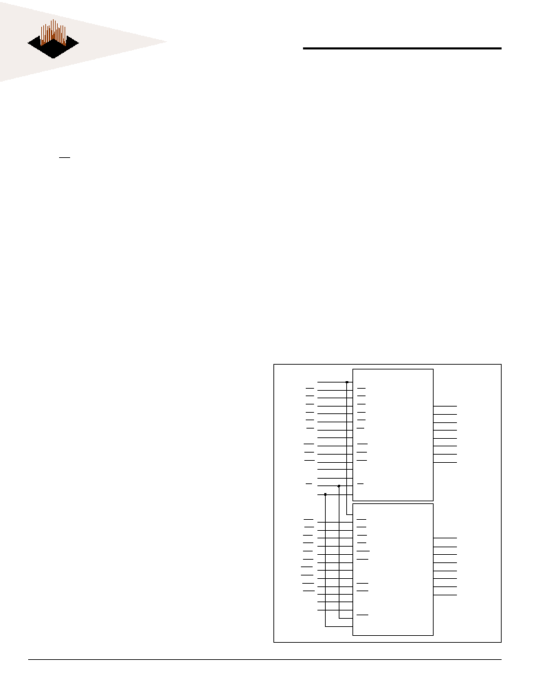
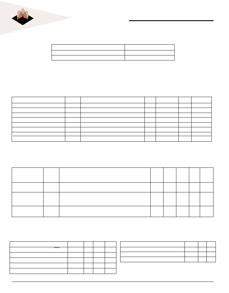
512K x 72 Synchronous Pipeline Burst ZBL SRAM
May 2003 Rev. 5
F
UNCTIONAL
B
LOCK
D
IAGRAM
*PRELIMINARY
FEATURES
DESCRIPTION
BENEFITS
n
30% space savings compared to equivalent TQFP
solution
n
Reduced part count
n
24% I/O reduction
n
Laminate interposer for optimum TCE match
n
Low Profile
n
Reduce layer count for board routing
n
Suitable for hi-reliability applications
n
User configurable as 1M x 36 or 2M x 18
n
Upgradable to 1M x 72 (contact factory for availability)
The WEDC SyncBurst - SRAM employs high-speed, low-
power CMOS design that is fabricated using an advanced
CMOS process. WEDCs 32Mb SyncBurst SRAMs integrate
two 512K x 36 SSRAMs into a single BGA package to pro-
vide 512K x 72 configuration. All synchronous inputs pass
through registers controlled by a positive-edge-triggered
single-clock input (CLK). The ZBL or Zero Bus Latency
Memory utilizes all the bandwidth in any combination of
operating cycles. Address, data inputs, and all control sig-
nals except output enable and linear burst order are syn-
chronized to input clock. Burst order control must be tied
High or Low. Asynchronous inputs include the sleep
mode enable (ZZ). Output Enable controls the outputs at
any given time. Write cycles are internally self-timed and
initiated by the rising edge of the clock input. This feature
eliminates complex off-chip write pulse generation and pro-
vides increased timing flexibility for incoming signals.
*Preliminary product that is not fully characterized, non-qualified and is subject
to change without notice.
A
0-18
BWa
BWb
BWc
BWd
WE
0
OE
0
CLK
0
CKE
0
CS1
0
CS2
0
CS2
0
ADV
0
LBO
ZZ
SA
BWa
BWb
BWc
BWd
WE
0
OE
0
CLK
CKE
CS1
CS2
CS2
ADV
LBO
ZZ
DQPA
DQA
0-7
DQPB
DQB
0-7
DQPC
DQC
0-7
DQPD
DQD
0-7
DQPA
DQA
0-7
DQPB
DQB
0-7
DQPC
DQC
0-7
DQPD
DQD
0-7
512K x 36 SSRAM
BWe
BWf
BWg
BWh
WE1
OE1
CLK1
CKE1
CS1
1
CS2
1
CS2
1
ADV1
SA
BWa
BWb
BWc
BWd
WEO
OEO
CLK
CKE
CS1
CS2
CS2
ADV
LBO
ZZ
512K x 36 SSRAM
DQPA
DQA
0-7
DQPB
DQB
0-7
DQPC
DQC
0-7
DQPH
DQD
0-7
DQPE
DQE
0-7
DQPF
DQF
0-7
DQPG
DQG
0-7
DQPH
DQH
0-7
2
White Electronic Designs Corporation (602) 437-1520 www.whiteedc.com
WEDPZ512K72S-XBX
White Electronic Designs
P
IN
C
ONFIGURATION
(TOP VIEW)
NOTE: DNU means Do Not Use and are reserved for future use.
* Pin F
8
reserved for A
19
upgrade to 1M x 72.
1
2
3
4
5
6
7
8
9
A
-
ADV
0
OE
0
DQB
2
DQB
4
DQB
6
DNU
DQA
6
DQA
2
B
CKE
0
WE
0
DQB
7
DQB
5
DQB
3
DQB
0
DQA
7
DQA
3
DQA
1
C
CLK
0
CS2
0
DQC
2
DQPC
DQPB
DQB
1
DQD
7
DQA
4
DQA
0
D
BWa
BWb
DQC
3
V
SS
V
SS
V
SS
DQD
6
DQA
5
DQPA
E
BWc
BWd
DQC
4
V
DDQ
V
DDQ
V
DDQ
DQD
5
DQPD
ZZ
F
CS1
0
CS2
0
DQC
5
V
DDQ
V
DDQ
V
SS
DQD
4
DNU*
A
0
G
A
7
DQC
0
DQC
7
V
SS
V
DD
V
DD
DQD
3
A
1
A
3
H
A
18
DQC
1
DQC
6
V
DD
V
DD
V
DD
`
DQD
2
A
2
A
5
J
A
9
A
6
DQF
2
V
SS
V
SS
V
SS
DQD
1
A
4
A
16
K
A
8
DQF
4
FQF
3
V
DD
V
DD
V
DD
DQD
0
A
14
A
15
L
A
17
DQF
5
DQF
6
V
DD
V
DD
V
SS
DQE
6
A
12
A
13
M
ADV
1
OE
1
DQF
7
V
SS
V
DDQ
V
DDQ
DQE
7
A
10
A
11
N
CKE
1
WE
1
DQPF
V
DDQ
V
DDQ
V
DDQ
DQE
5
DQE
3
LBO
P
CLK
1
CS2
1
DQF
1
V
SS
V
SS
V
SS
DQE
4
DQE
2
DQE
0
R
BWe
BWfDQF
0
DQG
1
DQG
4
DQH
1
DQH
2
DQE
1
DQPE
T
BWg
BWh
DQG
0
DQG
2
DQG
5
DQH
0
DQH
4
DQH
7
DQPH
U
CS1
1
CS2
1
DQG
3
DQPG
DQG
6
DQG
7
DQH
3
DQH
5
DQH
6
3
White Electronic Designs Corporation (602) 437-1520 www.whiteedc.com
White Electronic Designs
WEDPZ512K72S-XBX
BURST SEQUENCE TABLE
NOTE 1: LBO pin must be tied to High or Low, and Floating State must not be allowed.
Write operation occurs when WE is driven low at the
rising edge of the clock. BW[h:a] can be used for byte
write operation. The pipe-lined ZBL SSRAM uses a
late-late write cycle to utilize 100% of the bandwidth. At
the first rising edge of the clock, WE and address are
registered, and the data associated with that address
is required two cycles later.
Subsequent addresses are generated by ADV High for
the burst access as shown below. The starting point of
the burst seguence is provided by the external address.
The burst address counter wraps around to its initial
state upon completion. The burst sequence is deter-
mined by the state of the LBO pin. When this pin is low,
linear burst sequence is selected. And when this pin is
high, Interleaved burst sequence is selected.
During normal operation, ZZ must be driven low. When
ZZ is driven high, the SRAM will enter a Power Sleep
Mode after two cycles. At this time, internal state of the
SRAM is preserved. When ZZ returns to low, the SRAM
operates after two cycles of wake up time.
(Interleaved Burst, LBO = High)
Case 1 Case 2 Case 3 Case 4
LBO Pin High A1 A0 A1 A0 A1 A0 A1 A0
First Address
0
0
0
1
1
0
1
1
0
1
0
0
1
1
1
0
1
0
1
1
0
0
0
1
Fourth Address 1
1
1
0
0
1
0
0
(Linear Burst, LBO = Low)
Case 1 Case 2 Case 3 Case 4
LBO Pin High A1 A0 A1 A0 A1 A0 A1 A0
First Address
0
0
0
1
1
0
1
1
0
1
1
0
1
1
0
0
1
0
1
1
0
0
0
1
Fourth Address 1
1
0
0
0
1
1
0
The WEDPZ512K72S-XBX is an ZBL SSRAM designed
to sustain 100% bus bandwidth by eliminating turn-
around cycle when there is transition from Read to
Write, or vice versa. All inputs (with the exception of OE,
LBO and ZZ) are synchronized to rising clock edges.
All read, write and deselect cycles are initiated by the
ADV input. Subsequent burst addresses can be inter-
nally generated by the burst advance pin (ADV). ADV
should be driven to Low once the device has been
deselected in order to load a new address for next
operation.
Clock Enable (CKE) pin allows the operation of the
chip to be suspended as long as necessary. When
CKE is high, all synchronous inputs are ignored and
the internal device registers will hold their previous
values. NBL SSRAM latches external address and ini-
tiates a cycle when CKE and ADV are driven low at the
rising edge of the clock.
Output Enable (OE) can be used to disable the output at
any given time. Read operation is initiated when at the
rising edge of the clock, the address presented to the
address inputs are latched in the address register, CKE
is driven low, the write enable input signals WE are
driven high, and ADV driven low. The internal array is
read between the first rising edge and the second ris-
ing edge of the clock and the data is latched in the out-
put register. At the second clock edge the data is driven
out of the SRAM. During read operation OE must be
driven low for the device to drive out the requested data.
FUNCTION DESCRIPTION
4
White Electronic Designs Corporation (602) 437-1520 www.whiteedc.com
WEDPZ512K72S-XBX
White Electronic Designs
TRUTH TABLES
S
YNCHRONOUS
T
RUTH
T
ABLE
W
RITE
T
RUTH
T
ABLE
WE
BWa
BWb
BWc
BWd
Operation
H
X
X
X
X
Read
L
L
H
H
H
Write Byte a
L
H
L
H
H
Write Byte b
L
H
H
L
H
Write Byte c
L
H
H
H
L
Write Byte d
L
L
L
L
L
Write All Bytes
L
H
H
H
H
Write Abort/NOP
CEx ADVWE BWx OE
CKE CLK Address Accessed
Operation
H
L
X
X
X
L
N/A
Deselect
X
H
X
X
X
L
N/A
Continue Deselect
L
L
H
X
L
L
External Address
Begin Burst Read Cycle
X
H
X
X
L
L
Next Address
Continue Burst Read Cycle
L
L
H
X
H
L
External Address
NOP/Dummy Read
X
H
X
X
H
L
Next Address
Dummy Read
L
L
L
L
X
L
External Address
Begin Burst Write Cycle
X
H
X
L
X
L
Next Address
Continue Burst Write Cycle
L
L
L
H
X
L
N/A
NOP/Write Abort
X
H
X
H
X
L
Next Address
Write Abort
X
X
X
X
X
H
Current Address
Ignore Clock
NOTES:
1. X means Dont Care.
2. The rising edge of clock is symbolized by ( ).
3. A continue deselect cycle can only be entered if a deselect cycle is executed first.
4. WRITE = L means Write operation in WRITE TRUTH TABLE.
WRITE = H means Read operation in WRITE TRUTH TABLE.
5. Operation finally depends on status of asynchronous input pins (ZZ and OE).
6. CEx refers to the combination of CS
1
, CS
2
and CS
2
.
NOTES:
1. X means Dont Care.
2. All inputs in this table must meet setup and hold time around the rising edge of CLK ( ).
3. Replace BW
A
with BW
E
, BW
B
, with BW
F
, BW
C
with BW
G
and BW
D
with BW
H
for operation of IC
2
.
5
White Electronic Designs Corporation (602) 437-1520 www.whiteedc.com
White Electronic Designs
WEDPZ512K72S-XBX
150
133
100
Description
Symbol Conditions
MHz
MHz
MHz Units Notes
(Max) (Max) (Max)
Power Supply
I
DD
Device Selected; All Inputs £ V
IL
or ≥ V
IH
; Cycle
700
650
600
mA
1
Current: Operating
Time ≥ T
CYC
MIN; V
DD
= MAX; Output Open
Power Supply
I
SB2
Device Deselected; V
DD
= MAX; All Inputs £ V
IL or
≥ V
IH
Current: Standby
All Inputs Static; CLK Frequency = MAX
120
120
120
mA
Output Open, ZZ ≥ V
DD -
0.2V
Clock Running
I
SB
Device Deselected; V
DD
= MAX; All Inputs
180
180
160
mA
Standby Current
£ V
SS
+ 0.2 or V
DD
- 0.2; f = max ; ZZ £ V
IL
A
BSOLUTE
M
AXIMUM
R
ATINGS
*
V
IN
Voltage or any other pin relative to V
SS
-0.3V to +3.6V
Voltage on V
DD
supply relative to V
SS
-0.3V to +3.6V
Storage temperature (BGA)
-55∞C to +150∞C
E
LECTRICAL
C
HARACTERISTICS
(-55∞C TA +125∞C)
*Stress greater than those listed under Absolute Maximum Ratings: may cause
permanent damage to the device. This is a stress rating only and functional operation
of the device at these or any other conditions greater than those indicated in the
operational sections of this specification is not implied. Exposure to absolute maximum
rating condtions for extended periods may affect reliability.
Description
Symbol
Conditions
Min
Max
Units
Notes
Input High (Logic 1) Voltage
V
IH
1.7
V
DD
+0.3
V
1
Input Low (Logic 0) Voltage
V
IL
-0.3
0.7
V
1
Input Leakage Current
I
IL
V
DD =
M
ax,
0V V
IN
V
DD
-4
+4
µA
2
Output Leakage Current
I
LO
Output(s) Disabled, V
OUT
= V
SS
to V
DDQ
-2
+2
µA
Output High Voltage
V
OH
I
OH
= -1.0mA
2.0
---
V
1
Output Low Voltage
V
OL
I
OL
= 1.0mA
---
0.4
V
1
Supply Voltage
V
DD
2.375
2.625
V
1
I/O Power Suply
V
DDQ
2.375
2.625
V
1
NOTES:
1. All voltages referenced to V
SS
(GND)
2. ZZ pin has an internal pull-up, and input leakage = ± 20 µA.
DC C
HARACTERISTICS
(-55∞C TA + 125∞C)
BGA C
APACITANCE
(T
A
= + 25∞C, f = 1MH
Z
)
NOTES: 1. This parameter is not tested but guaranteed by design.
Description
Symbol Max Units Notes
Control Input Capacitance (LBO, zz)
C
IC
16
pF
1
Control Input Capacitance
C
I
8
pF
1
Input/Output Capacitance (DQ)
C
O
10
pF
1
Address Capacitance
C
A
16
pF
1
Clock Capacitance
C
CK
6
pF
1
NOTES: 1. I
DD
is specified with no output current and increases with faster cycle times.
I
DD
increases with faster cycle times and greater output loading.
T
HERMAL
R
ESISTANCE
Parameter
Symbol Max Unit
Thermal Resistance: Die Junction to Ambient
qJA
28.7 ∞C/W
Thermal Resistance: Die Junction to Ball
qJB
16.0 ∞C/W
Thermal Resistance: Die Junction to Case
qJC
7.1 ∞C/W
Note: Refer to Application Note PBGA Thermal Resistance Corrleation
for further information regarding WEDCs thermal modeling.
6
White Electronic Designs Corporation (602) 437-1520 www.whiteedc.com
WEDPZ512K72S-XBX
White Electronic Designs
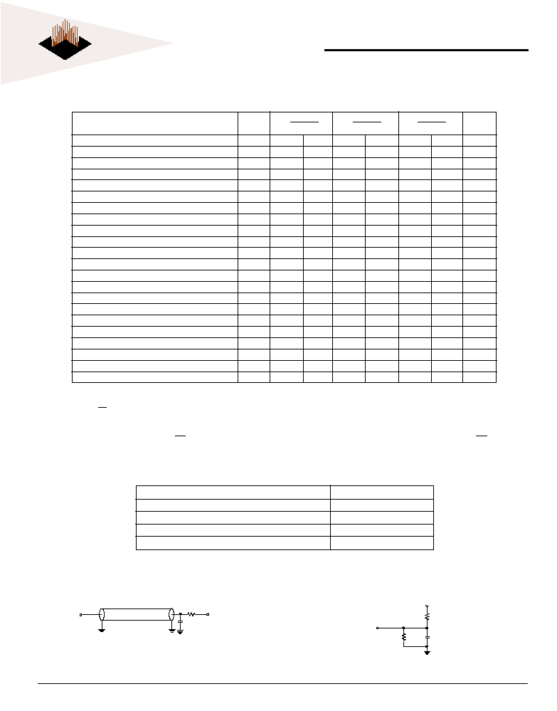
AC C
HARACTERISTICS
(-55∞C T
A
+125∞C)
NOTES:
1. All Address inputs must meet the specified setup and hold times for all rising clock (CLK) edges when ADV is sampled low
and CSx is sampled valid. All other synchronous inputs must meet the specified setup and hold times whenever this
device is chip selected.
2. Chip enable must be valid at each rising edge of CLK (when ADV is Low) to remain enabled.
3. A write cycle is defined by WE low having been registered into the device at ADV Low. A Read cycle is defined by WE
High with ADV Low. Both cases must meet setup and hold times.
O
UTPUT
L
OAD
(A)
O
UTPUT
L
OAD
(B)
(FOR T
LZC
, T
LZOE
, T
HZOE
,
AND
T
HZC
)
Dout
Zo=50
RL=50
VL=1.25V
50pF*
Dout
1538
5pF*
+2.5V
1667
*Including Scope and Jig Capacitance
AC T
EST
C
ONDITIONS
Parameter
Value
Input Pulse Level
0 to 2.5V
Input Rise and Fall Time
1.0V/ns
Input and Output Timing Reference Levels
1.25V
Output Load
See Output Load (A & B)
Symbol
150MHz
133MHz
100MHz
Parameter
Min
Max
Min
Max
Min
Max
Units
Clock Time
t
C Y C
6.7
7.5
10.0
n s
Clock Access Time
t
CD
--
3.8
--
4.2
--
5.0
n s
Output enable to Data Valid
t
OE
--
3.8
--
4.2
--
5.0
n s
Clock High to Output Low-Z
t
L Z C
1.5
--
1.5
--
1.5
--
n s
Output Hold from Clock High
t
OH
1.5
--
1.5
--
1.5
--
n s
Output Enable Low to output Low-Z
t
LZOE
0.0
--
0.0
--
0.0
--
n s
Output Enable High to Output High-Z
t
HZOE
--
3.0
--
3.5
--
3.5
n s
Clock High to Output High-Z
t
HZC
--
3.0
--
3.5
--
3.5
n s
Clock High Pulse Width
t
CH
2.5
--
2.5
--
3.0
--
n s
Clock Low Pulse Width
t
CL
2.5
--
2.5
--
3.0
--
n s
Address Setup to Clock High
t
A S
1.5
--
1.5
--
1.5
--
n s
CKE Setup to Clock High
t
C E S
1.5
--
1.5
--
1.5
--
n s
Data Setup to Clock High
t
D S
1.5
--
1.5
--
1.5
--
n s
Write Setup to Clock High
t
WS
1.5
--
1.5
--
1.5
--
n s
Address Advance to Clock High
t
A D V S
1.5
1.5
1.5
n s
Chip Select Setup to Clock High
t
C S S
1.5
1.5
1.5
n s
Address Hold to Clock high
t
A H
0.5
--
0.5
--
0.5
--
n s
CKE Hold to Clock High
t
C E H
0.5
--
0.5
--
0.5
--
n s
Data Hold to Clock High
t
DH
0.5
--
0.5
--
0.5
--
n s
Write Hold to Clock High
t
WH
0.5
--
0.5
--
0.5
--
n s
Address Advance to Clock High
t
ADVH
0.5
--
0.5
--
0.5
--
n s
Chip Select Hold to Clock High
t
C S H
0.5
--
0.5
---
0.5
--
n s
7
White Electronic Designs Corporation (602) 437-1520 www.whiteedc.com
White Electronic Designs
WEDPZ512K72S-XBX
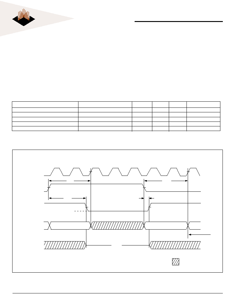
SNOOZE MODE is a low-current, power-down mode
in which the device is deselected and current is re-
duced to ISB
2
Z
. The duration of SNOOZE MODE is
dictated by the length of time Z is in a HIGH state. After
the device enters SNOOZE MODE, all inputs except ZZ
become gated inputs and are ignored. ZZ is an asyn-
chronous, active HIGH input that causes the device to
enter SNOOZE MODE.
When ZZ becomes a logic HIGH, ISB
2
Z
is guaranteed
after the setup time t
ZZ
is met. Any READ or WRITE
operation pending when the device enters SNOOZE
MODE is not guaranteed to complete successfully.
Therefore, SNOOZE MODE must not be initiated until
valid pending operations are completed.
S
NOOZE
M
ODE
Description
Conditions
Symbol
Min
Max
Units
Current during SNOOZE MODE
ZZ ≥ V
IH
I
SB2Z
20
mA
ZZ active to input ignored
tzz
2
cycle
ZZ inactive to input sampled
trzz
2
cycle
ZZ active to snooze current
t
ZZI
2
cycle
ZZ inactive to exit snooze current
t
RZZI
O
ns
FIG. 2
SNOOZE MODE
S
NOOZE
M
ODE
T
IMING
D
IAGRAM
ZZ
I
SUPPLY
CLOCK
ALL INPUTS
(except ZZ)
Output (Q)
t
ZZ
t
ZZI
t
RZZ
t
RZZI
HIGH-Z
DESELECT or READ Only
I
ISB2Z
DON'T CARE
Deselect or Read Only
Normal
Operation Cycle
8
White Electronic Designs Corporation (602) 437-1520 www.whiteedc.com
WEDPZ512K72S-XBX
White Electronic Designs
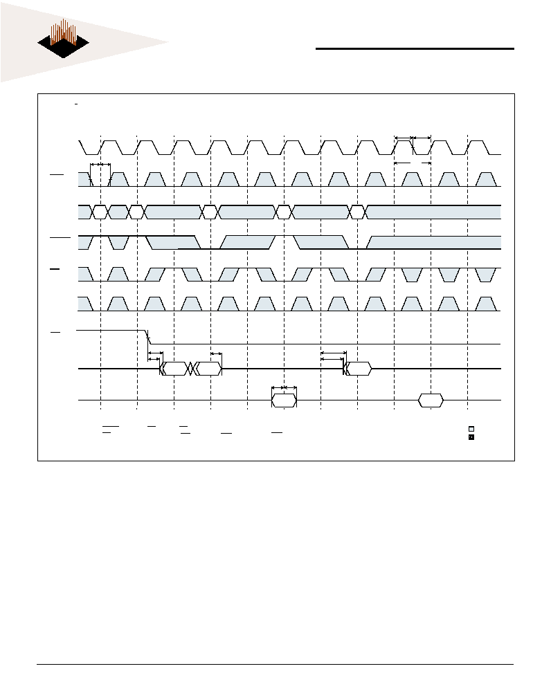
FIG. 3
T
IMING
W
AVEFORM
OF
R
EAD
C
YCLE
CLK
x
CKE
x
Address
WRITE
ADV
x
OE
Data Out
t
CH
t
CL
t
CES
t
CEH
t
AS
t
AH
A1
A2
A3
t
WS
t
WH
t
CSS
t
CSH
t
OE
t
HZOE
t
LZOE
t
CD
t
OH
t
HZC
Q3-4
Q3-3
Q3-2
Q3-1
Q2-4
Q2-3
Q2-2
Q2-1
Q1-1
Don¢t Care
Undefined
t
CYC
t
ADVS
t
ADVH
CSx
NOTES:
WRITE = L means WEx = L, and BWx = L
CSx refers to the combination of CS10, CS20 and CS20, or CS11, CS21 and CS21.
9
White Electronic Designs Corporation (602) 437-1520 www.whiteedc.com
White Electronic Designs
WEDPZ512K72S-XBX
FIG. 4
T
IMING
W
AVEFORM
OF
W
RITE
C
YCLE
CLKx
Address
WRITE
ADVx
Data In
t
CH
t
CL
A2
A3
D2-1
D1-1
D2-2
D2-3
D2-4
D3-1
D3-2
D3-3
OE
Data Out
t
DS
t
DH
Don¢t Care
Undefined
t
CYC
CKEx
A1
D3-4
t
CES
t
CEH
Q0-4
t
HZOE
Q0-3
CSx
NOTES:
WRITE = L means WEx = L, and BWx = L
CSx refers to the combination of CS1
0,
CS2
0
and CS2
0,
or CS1
1,
CS2
1
and CS2
1.
10
White Electronic Designs Corporation (602) 437-1520 www.whiteedc.com
WEDPZ512K72S-XBX
White Electronic Designs
CLKx
Address
WRITE
ADVx
OE
Data In
t
CH
t
CL
t
DS
t
DH
Data Out
A2
A4
A5
D2
t
OE
t
LZOE
Q1
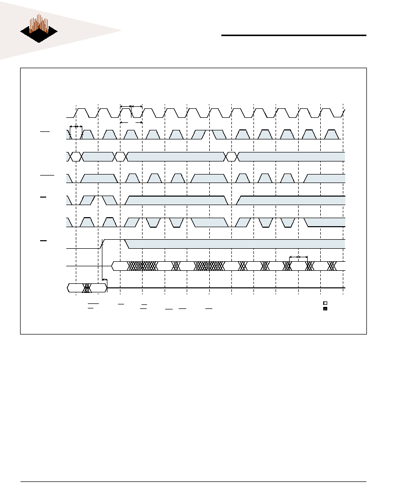
Don¢t Care
Undefined
t
CYC
CKEx
t
CES
t
CEH
A1
A3
A7
A6
Q3
Q4
Q7
Q6
D5
A9
A8
CSx
NOTES:
WRITE = L means WE
x
= L, and BWx = L
CSx refers to the combination of
CS1
0,
CS2
0
and CS2
0,
or CS1
1,
CS2
1
and CS2
1.
FIG. 5
T
IMING
W
AVEFORM
OF
S
INGLE
R
EAD
/W
RITE
11
White Electronic Designs Corporation (602) 437-1520 www.whiteedc.com
White Electronic Designs
WEDPZ512K72S-XBX
FIG. 6
T
IMING
W
AVEFORM
OF
CKE O
PERATION
CLKx
Address
WRITE
ADV
x
OE
Data In
t
CH
t
CL
Data Out
A1
A2
A3
A4
A5
t
CES
t
CEH
Don¢t Care
Undefined
t
CYC
CKE
x
t
DS
t
DH
D2
Q4
Q1
t
CD
t
LZC
t
HZC
Q3
A6
CSx
NOTES:
WRITE = L means WE = L, and BWx = L
CSx refers to the combination of CS10, CS20 and CS20, or CS11, CS21 and CS21.
12
White Electronic Designs Corporation (602) 437-1520 www.whiteedc.com
WEDPZ512K72S-XBX
White Electronic Designs
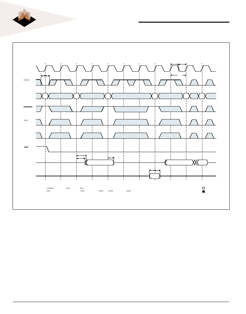
FIG. 7
T
IMING
W
AVEFORM
OF
CE O
PERATION
CLK
X
Address
WRITE
ADV
X
OE
Data In
t
CH
t
CL
Data Out
A1
A2
A3
A4
A5
Don¢t Care
Undefined
t
CYC
CKE
X
D5
Q4
t
CES
t
CEH
Q1
Q2
t
OE
t
LZOE
D3
t
CD
t
LZC
t
HZC
t
DH
t
DS
CS
X
NOTES:
WRITE = L means WE = L, and BWx = L
CSx refers to the combination of CS1
0
, CS2
0
and CS2
0
, or CS1
1
, and CS2
1
.
13
White Electronic Designs Corporation (602) 437-1520 www.whiteedc.com
White Electronic Designs
WEDPZ512K72S-XBX
0.61 (0.024) ± 0.08 (0.003)
BSC
1.27
(0.050)
BSC
A
B
C
D
E
F
G
H
J
K
L
M
N
P
R
T
U
20.32 (0.800)
BSC
9 8 7 6 5 4 3 2 1
23.20 (0.913)
MAX
17.2 (0.677)
MAX
10.16 (0.400)
BSC
2.20 (0.087)
MAX
BOTTOM VIEW
0.76 (0.030) ± 0.08 (0.003)
DEVICE GRADE:
M = Military
-55∞C to +125∞C
I = Industrial
-40∞C to +85∞C
C = Commercial
0∞C to +70∞C
PACKAGE:
B = 152 Plastic Ball Grid Array (PBGA)
FREQUENCY (MHz)
100 = 100MHz
133 = 133MHz
150 = 150MHz
2.5 V Voltage
CONFIGURATION, 512K x 72
SSRAM ZBL
PLASTIC
WHITE ELECTRONIC DESIGNS CORP.
ALL LINEAR DIMENSIONS ARE IN MILLIMETERS AND PARENTHETICALLY IN INCHES
WED P Z 512K 72 S - XXX B X
ORDERING INFORMATION
PACKAGE DIMENSION:
152 BUMP PBGA

14
White Electronic Designs Corporation (602) 437-1520 www.whiteedc.com
WEDPZ512K72S-XBX
White Electronic Designs
Document Title
512K x 72 Synchronous SRAM NBL
Revision History
Rev #
History
Release Date
Status
Rev 0
Initial Release
February 2001
Advanced
Rev 1
Changes (Pg. 1, 5, 6, 13)
April 2001
Advanced
1.1 Block Diagram: Change DQD to DQPD, Font Consistency
1.2 Electrical Characteristics Note 2: Change reference to mA instead of MA.
1.3 DC Characteristics: Adjust location of Units & Notes for ISB2.
1.4 AC Characteristics: Change temperature range to (-55∞C £ T
A
£ +125∞C)
1.5 Package Dimension: Adjust length line to end of package
1.6 Block Diagram: Adjust look for consistency
1.7 DC Characteristics: ISB2 condition should read All Inputs £ V
IL
or ≥ V
IH
instead of > V
IH
1.8 Figure 2: Inputs transition should not be shown fully connected.
1.9 Figure 6: Unknown text deleted from timing diagram
1.10 Package Dimension: Ball diameter arrow corrected to point to ball.
Rev 2
Change (1)
November 2001
Preliminary
1.1 Change status from Advanced to Preliminary
Rev 3
Changes (1, 2)
November 2001
Preliminary
1.1 Block Diagram: Address lines should be A0-18
1.2 Pin Configuration: Add Note *Pin F8 reserved for A19 upgrade to 1Mx72.
Rev 4
Changes (1, 5)
November 2002
Preliminary
1.1 BGA Capacitance: Remove references to temperature in individual conditions
1.2 Change C
I
from 10pF to 8pF
1.3 Change C
A
from 20pF to 16pF
1.4 Change C
CK
from 7pF to 6pF
1.5 Add Control Input Capacitance (C
IC
) 16pF
Rev 5
Changes (5)
May 2003
Preliminary
Add Thermal Resistance table
Update current values
Update package mechanical drawing