
WEDPZ512K72S-XBX
1
White Electronic Designs Corporation ∑ (602) 437-1520 ∑ www.wedc.com
White Electronic Designs
PRELIMINARY*
White Electronic Designs Corp. reserves the right to change products or specifi cations without notice.
November 2003
Rev. 6
Fast clock speed: 150, 133, and 100MHz
Fast access times: 3.8ns, 4.2ns, and 5.0ns
Fast OE# access times: 3.8ns, 4.2ns, and 5.0ns
High performance 3-1-1-1 access rate
2.5V ± 5% power supply
Common data inputs and data outputs
Byte write enable and global write control
Six chip enables for depth expansion and address
pipeline
Internally self-timed write cycle
Burst control pin (interleaved or linear burst
sequence)
Automatic power-down for portable applications
Commercial, industrial and military temperature
ranges
Packaging:
∑ 152 PBGA package 17 x 23mm
512K x 72 SYNCHRONOUS PIPELINE BURST ZBL SRAM
FEATURES
DESCRIPTION
BENEFITS
30% space savings compared to equivalent TQFP
solution
Reduced part count
24%
I/O
reduction
Laminate interposer for optimum TCE match
Low
Profi
le
Reduce layer count for board routing
Suitable for hi-reliability applications
User confi gurable as 1M x 36 or 2M x 18
Upgradable to 1M x 72 (contact factory for
availability)
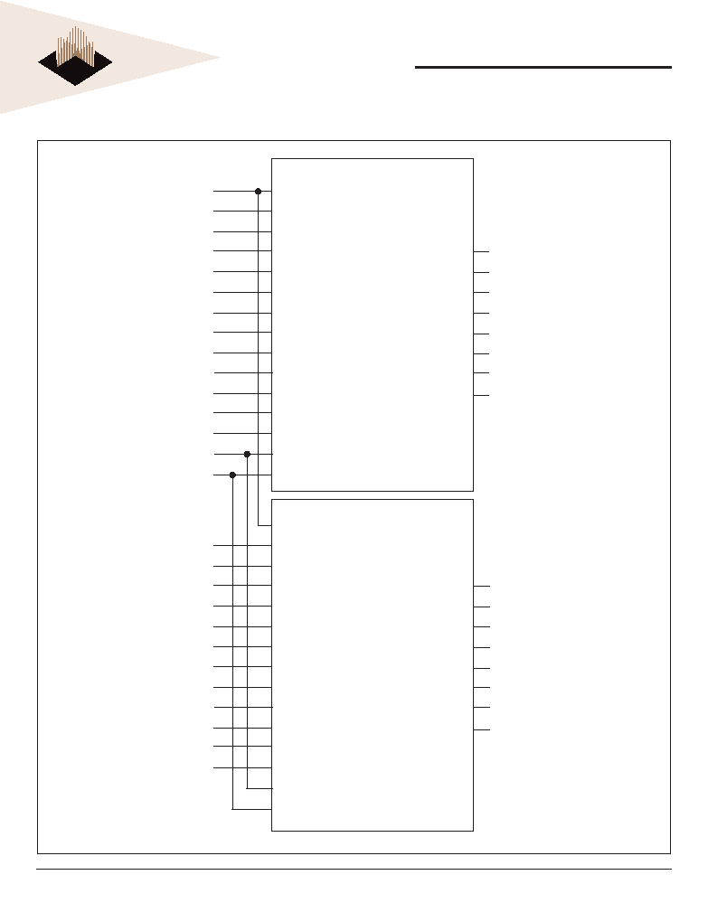
The WEDC SyncBurst - SRAM employs high-speed,
low-power CMOS design that is fabricated using an
advanced CMOS process. WEDC's 32Mb SyncBurst
SRAMs integrate two 512K x 36 SSRAMs into a single
BGA package to provide 512K x 72 confi guration. All
synchronous inputs pass through registers controlled by a
positive-edge-triggered single-clock input (CLK). The ZBL
or Zero Bus Latency Memory utilizes all the bandwidth
in any combination of operating cycles. Address, data
inputs, and all control signals except output enable and
linear burst order are synchronized to input clock. Burst
order control must be tied "High or Low." Asynchronous
inputs include the sleep mode enable (ZZ). Output Enable
controls the outputs at any given time. Write cycles are
internally self-timed and initiated by the rising edge of the
clock input. This feature eliminates complex off-chip write
pulse generation and provides increased timing fl exibility
for incoming signals.
* This product is under development, is not qualifi ed or characterized and is subject to
change without notice.
WEDPZ512K72S-XBX
2
White Electronic Designs Corporation ∑ (602) 437-1520 ∑ www.wedc.com
White Electronic Designs
PRELIMINARY*
White Electronic Designs Corp. reserves the right to change products or specifi cations without notice.
November 2003
Rev. 6
FUNCTIONAL BLOCK DIAGRAM
A0-18
BW
a
#
BW
b
#
BW
c
#
BW
d
#
WE
0
#
OE
0
#
CLK
0
#
CKE
0
#
CS
10
#
CS
20
#
CS
20
ADV
0
LB
0
#
ZZ
SA
BW
a
#
BW
b
#
BW
c
#
BW
d
#
WE
0
#
OE
0
#
CLK
CKE#
CS
1
#
CS
2
#
CS
2
ADV
LB
0
#
ZZ
DQPA
DQA
0-7
DQPB
DQB
0-7
DQPC
DQC
0-7
DQPD
DQD
0-7
DQPA
DQA
0-7
DQPB
DQB
0-7
DQPC
DQC
0-7
DQPD
DQD
0-7
512K x 36 SSRAM
BW
e
#
BW
f
#
BW
g
#
BW
h
#
WE
1
#
OE
1
#
CLK
1
#
CKE
1
#
CS
113
#
CS
21
#
CS
21
#
ADV
1
SA
BW
a
#
BW
b
#
BW
c
#
BW
d
#
WE
0
#
OE
0
#
CLK
CKE
CS
1
#
CS
2
#
CS
2
ADV
LB
0
#
ZZ
512K x 36 SSRAM
DQPA
DQA
0-7
DQPB
DQB
0-7
DQPC
DQC
0-7
DQPH
DQD
0-7
DQPE
DQE
0-7
DQPF
DQF
0-7
DQPG
DQG
0-7
DQPH
DQH
0-7

WEDPZ512K72S-XBX
3
White Electronic Designs Corporation ∑ (602) 437-1520 ∑ www.wedc.com
White Electronic Designs
PRELIMINARY*
White Electronic Designs Corp. reserves the right to change products or specifi cations without notice.
November 2003
Rev. 6
PIN CONFIGURATION
(TOP VIEW)
NOTES:
DNU means Do Not Use and are reserved for future use.
* Pin F8 reserved for A19 upgrade to 1M x 72.
1
2
3
4
5
6
7
8
9
A
-
ADV0
OE
0
#
DQB
2
DQB
4
DQB
6
DNU
DQA
6
DQA
2
B
CKE
0
#
WE
0
#
DQB
7
DQB
5
DQB
3
DQB
0
DQA
7
DQA
3
DQA
1
C
CLK
0
CS
20
#
DQC
2
DQPC
DQPB
DQB
1
DQD
7
DQA
4
DQA
0
D
BWA#
BWB#
DQC
3
V
SS
V
SS
V
SS
DQD
6
DQA
5
DQPA
E
BWC#
BWD#
DQC
4
V
CCQ
V
CCQ
V
CCQ
DQD
5
DQPD
ZZ
F
CS
10
#
CS
20
DQC
5
V
CCQ
V
CCQ
V
SS
DQD
4
DNU*
A
0
G
A
7
DQC
0
DQC
7
V
SS
V
CC
V
CC
DQD
3
A
1
A
3
H
A
18
DQC
1
DQC
6
V
CC
V
CC
V
CC
DQD
2
A
2
A
5
J
A
9
A
6
DQF
2
V
SS
V
SS
V
SS
DQD
1
A
4
A
16
K
A
8
DQF
4
DQF
3
V
CC
V
CC
V
CC
DQD
0
A
14
A
15
L
A
17
DQF
5
DQF
6
V
CC
V
CC
V
SS
DQE
6
A
12
A
13
M
ADV
1
OE
1
#
DQF
7
V
SS
V
CCQ
V
SSQ
DQE
7
A
10
A
11
N
CKE
1
#
WE
1
#
DQPF
V
CCQ
V
CCQ
V
CCQ
DQE
5
DQE
3
LBO#
P
CLK
1
CS
21
#
DQF
1
V
SS
V
SS
V
SS
DQE
4
DQE
2
DQE
0
R
BWE#
BWF#
DQF
0
DQG
1
DQG
4
DQH
1
DQH
2
DQE
1
DQPE
T
BWG#
BWH#
DQG
0
DQG
2
DQG
5
DQH
0
DQH
4
DQH
7
DQPH
U
CS
11
#
CS
21
DQG
3
DQPG
DQG
6
DQG
7
DQH
3
DQH
5
DQH
6

WEDPZ512K72S-XBX
4
White Electronic Designs Corporation ∑ (602) 437-1520 ∑ www.wedc.com
White Electronic Designs
PRELIMINARY*
White Electronic Designs Corp. reserves the right to change products or specifi cations without notice.
November 2003
Rev. 6
BURST SEQUENCE TABLE
NOTE: LBO pin must be tied to High or Low, and Floating State must not be allowed.
(Interleaved Burst, LBO# = High)
LBO# Pin
High
Case 1
Case 2
Case 3
Case 4
A1
A0
A1
A0
A1
A0
A1
A0
First Address
Fourth Address
0
0
0
1
1
0
1
1
0
1
0
0
1
1
1
0
1
0
1
1
0
0
0
1
1
1
1
0
0
1
0
0
(Linear Burst, LBO# = Low)
LBO# Pin
High
Case 1
Case 2
Case 3
Case 4
A1
A0
A1
A0
A1
A0
A1
A0
First Address
Fourth Address
0
0
0
1
1
0
1
1
0
1
1
0
1
1
0
0
1
0
1
1
0
0
0
1
1
1
0
0
0
1
1
0
The WEDPZ512K72S-XBX is an ZBL SSRAM designed
to sustain 100% bus bandwidth by eliminating turnaround
cycle when there is transition from Read to Write, or vice
versa. All inputs (with the exception of OE#, LBO# and ZZ)
are synchronized to rising clock edges.
All read, write and deselect cycles are initiated by the
ADV input. Subsequent burst addresses can be internally
generated by the burst advance pin (ADV). ADV should
be driven to Low once the device has been deselected in
order to load a new address for next operation.
Clock Enable (CKE#) pin allows the operation of the chip to
be suspended as long as necessary. When CKE# is high,
all synchronous inputs are ignored and the internal device
registers will hold their previous values. NBL SSRAM
latches external address and initiates a cycle when CKE
and ADV are driven low at the rising edge of the clock.
Output Enable (OE#) can be used to disable the output
at any given time. Read operation is initiated when at
the rising edge of the clock, the address presented to
the address inputs are latched in the address register,
CKE# is driven low, the write enable input signals WE#
are driven high, and ADV driven low. The internal array is
read between the fi rst rising edge and the second rising
edge of the clock and the data is latched in the output
register. At the second clock edge the data is driven out
of the SRAM. During read operation OE# must be driven
low for the device to drive out the requested data.
FUNCTION DESCRIPTION
Write operation occurs when WE# is driven low at the
rising edge of the clock. BW#[h:a] can be used for byte
write operation. The pipe-lined ZBL SSRAM uses a late-
late write cycle to utilize 100% of the bandwidth. At the fi rst
rising edge of the clock, WE# and address are registered,
and the data associated with that address is required two
cycles later.
Subsequent addresses are generated by ADV High for
the burst access as shown below. The starting point of the
burst seguence is provided by the external address. The
burst address counter wraps around to its initial state upon
completion. The burst sequence is determined by the state
of the LBO# pin. When this pin is low, linear burst sequence
is selected. And when this pin is high, Interleaved burst
sequence is selected.
During normal operation, ZZ must be driven low. When ZZ
is driven high, the SRAM will enter a Power Sleep Mode
after two cycles. At this time, internal state of the SRAM
is preserved. When ZZ returns to low, the SRAM operates
after two cycles of wake up time.

WEDPZ512K72S-XBX
5
White Electronic Designs Corporation ∑ (602) 437-1520 ∑ www.wedc.com
White Electronic Designs
PRELIMINARY*
White Electronic Designs Corp. reserves the right to change products or specifi cations without notice.
November 2003
Rev. 6
TRUTH TABLES
SYNCHRONOUS TRUTH TABLE
WRITE TRUTH TABLE
WE#
BW#a
BW#b
BW#c
BW#d
Operation
H
X
X
X
X
Read
L
L
H
H
H
Write Byte a
L
H
L
H
H
Write Byte b
L
H
H
L
H
Write Byte c
L
H
H
H
L
Write Byte d
L
L
L
L
L
Write All Bytes
L
H
H
H
H
Write Abort/NOP
CE#x
ADV
WE#
BW#x
OE#
CKE#
CLK
Address Accessed
Operation
H
L
X
X
X
L
N/A
Deselect
X
H
X
X
X
L
N/A
Continue Deselect
L
L
H
X
L
L
External Address
Begin Burst Read Cycle
X
H
X
X
L
L
Next Address
Continue Burst Read Cycle
L
L
H
X
H
L
External Address
NOP/Dummy Read
X
H
X
X
H
L
Next Address
Dummy Read
L
L
L
L
X
L
External Address
Begin Burst Write Cycle
X
H
X
L
X
L
Next Address
Continue Burst Write Cycle
L
L
L
H
X
L
N/A
NOP/Write Abort
X
H
X
H
X
L
Next Address
Write Abort
X
X
X
X
X
H
Current Address
Ignore Clock
NOTES:
1) X
means
"Don't
Care."
2)
The rising edge of clock is symbolized by ( ).
3)
A continue deselect cycle can only be entered if a deselect cycle is executed fi rst.
4)
WRITE# = L means Write operation in WRITE TRUTH TABLE.
WRITE# = H means Read operation in WRITE TRUTH TABLE.
5)
Operation fi nally depends on status of asynchronous input pins (ZZ and OE#).
6)
CE#x refers to the combination of CS#1 and CS#2.
NOTES:
1) X
means
"Don't
Care."
2)
All inputs in this table must meet setup and hold time around the rising edge of CLK ( ).
3)
Replace BW#a with BW#e, BW#b, with BW#f, BW#c with BW#g and BW#d with BW#h for
operation of IC2.