1
White Electronic Designs Corporation (602) 437-1520 www.whiteedc.com
WF128K32-XXX5
White Electronic Designs
I/O
8
I/O
9
I/O
10
A
14
A
16
A
11
A
0
NC
I/O
0
I/O
1
I/O
2
WE
2
CS
2
GND
I/O
11
A
10
A
9
A
15
V
CC
CS
1
NC
I/O
3
I/O
15
I/O
14
I/O
13
I/O
12
OE
NC
WE
1
I/O
7
I/O
6
I/O
5
I/O
4
I/O
24
I/O
25
I/O
26
A
7
A
12
NC
A
13
A
8
I/O
16
I/O
17
I/O
18
I/O
31
I/O
30
I/O
29
I/O
28
A
1
A
2
A
3
I/O
23
I/O
22
I/O
21
I/O
20
V
CC
CS
4
WE
4
I/O
27
A
4
A
5
A
6
WE
3
CS
3
GND
I/O
19
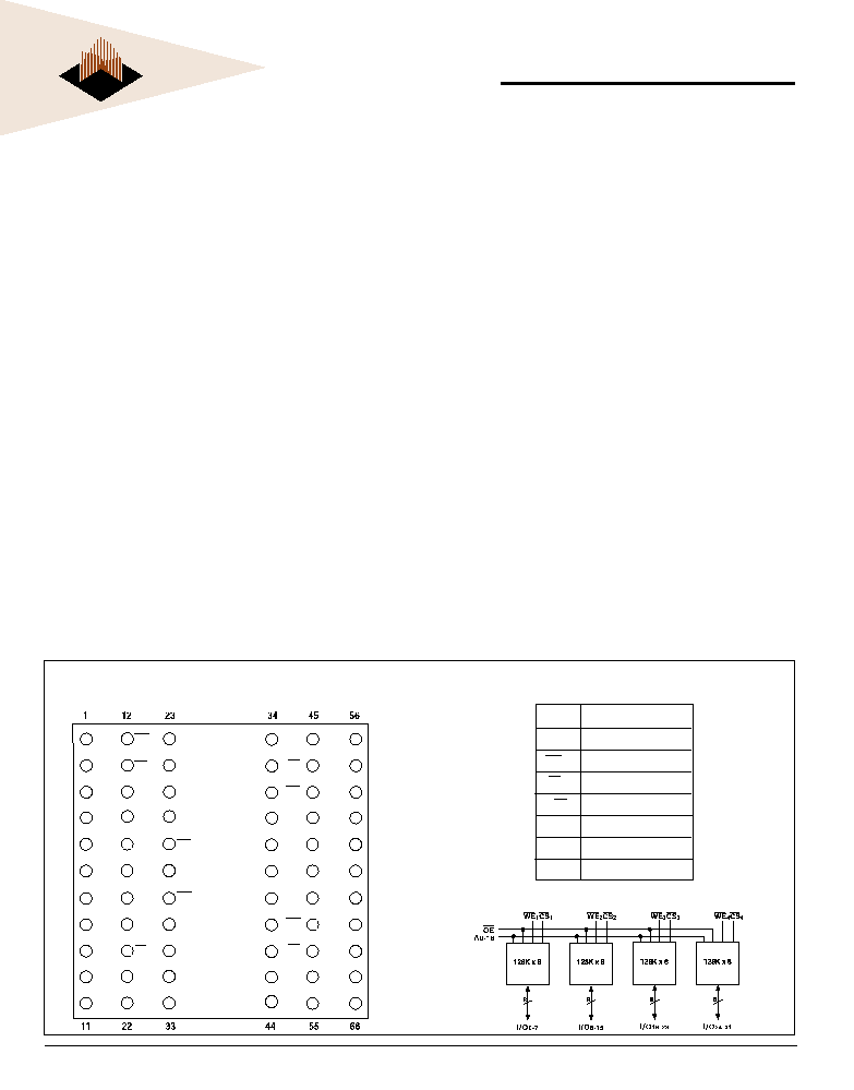
128K
X
32 5V FLASH MODULE, SMD 5962-94716
FEATURES
n
Access Times of 50*, 60, 70, 90, 120, 150ns
n
Packaging:
66 pin, PGA Type, 1.075 inch square, Hermetic
Ceramic HIP (Package 400)
68 lead, Hermetic CQFP (G2U), 22.4mm (0.880
inch) square, 3.56mm (0.140 inch) high
(Package 510)
68 lead, Hermetic CQFP (G2L), 22.4mm (0.880
inch) square, 4.06mm (0.160 inch) high (Pack
age 528)
68 lead, Hermetic CQFP (G1U)
1
, 23.9mm (0.940
inch) square, 3.56mm (0.140 inch) high
(Package 519)
68 lead, Hermetic CQFP (G1T), 23.9mm (0.940
inch) square, 4.06mm (0.160 inch) high
(Package 524)
n
Sector Architecture
8 equal size sectors of 16KBytes each
Any combination of sectors can be concurrently
erased. Also supports full chip erase
FIG. 1 PIN CONFIGURATION FOR WF128K32N-XH1X5
PIN DESCRIPTION
I/O
0-31
Data Inputs/Outputs
A
0-16
Address Inputs
WE
1-4
Write Enables
CS
1-4
Chip Selects
OE
Output Enable
V
CC
Power Supply
GND
Ground
NC
Not Connected
May 2003 Rev. 6
n
100,000 Erase/Program Cycles Typical, 0�C to +70�C
n
Organized as 128Kx32
n
Commercial, Industrial and Military Temperature
Ranges
n
5 Volt Programming. 5V � 10% Supply
n
Low Power CMOS, 1mA Standby Typical
n
Embedded Erase and Program Algorithms
n
TTL Compatible Inputs and CMOS Outputs
n
Built-in Decoupling Caps and Multiple Ground
Pins for Low Noise Operation
n
Page Program Operation and Internal Program
Control Time
n
Weight
WF128K32-XG2LX5 - 8 grams typical
WF128K32-XG1UX5
1
- 5 grams typical
WF128K32-XG1TX5 - 5 grams typical
WF128K32-XG2UX5 - 8 grams typical
WF128K32-XH1X5 - 13 grams typical
Note 1: Package Not Recommended For New Design
Note: For programming information refer to Flash Programming 1M5
Application Note.
* The access time of 50ns is available in Industrial and Commercial
temperature ranges only.
BLOCK DIAGRAM
TOP VIEW
2
White Electronic Designs Corporation Phoenix AZ (602) 437-1520
WF128K32-XXX5
White Electronic Designs
10
11
12
13
14
15
16
17
18
19
20
21
22
23
24
25
26
60
59
58
57
56
55
54
53
52
51
50
49
48
47
46
45
44
9 8 7 6 5 4 3 2 1 68 67 66 65 64 63 62 61
27 28 29 30 31 32 33 34 35 36 37 38 39 40 41 42 43
I/O
0
I/O
1
I/O
2
I/O
3
I/O
4
I/O
5
I/O
6
I/O
7
GND
I/O
8
I/O
9
I/O
10
I/O
11
I/O
12
I/O
13
I/O
14
I/O
15
V
CC
A
11
A
12
A
13
A
14
A
15
A
16
CS
1
OE
CS
2
NC
W
E
2
W
E
3
W
E
4
NC
NC
NC
I/O
16
I/O
17
I/O
18
I/O
19
I/O
20
I/O
21
I/O
22
I/O
23
GND
I/O
24
I/O
25
I/O
26
I/O
27
I/O
28
I/O
29
I/O
30
I/O
31
NC
A
0
A
1
A
2
A
3
A
4
A
5
CS
3
GN
D
CS
4
WE
1
A
6
A
7
A
8
A
9
A
10
V
CC
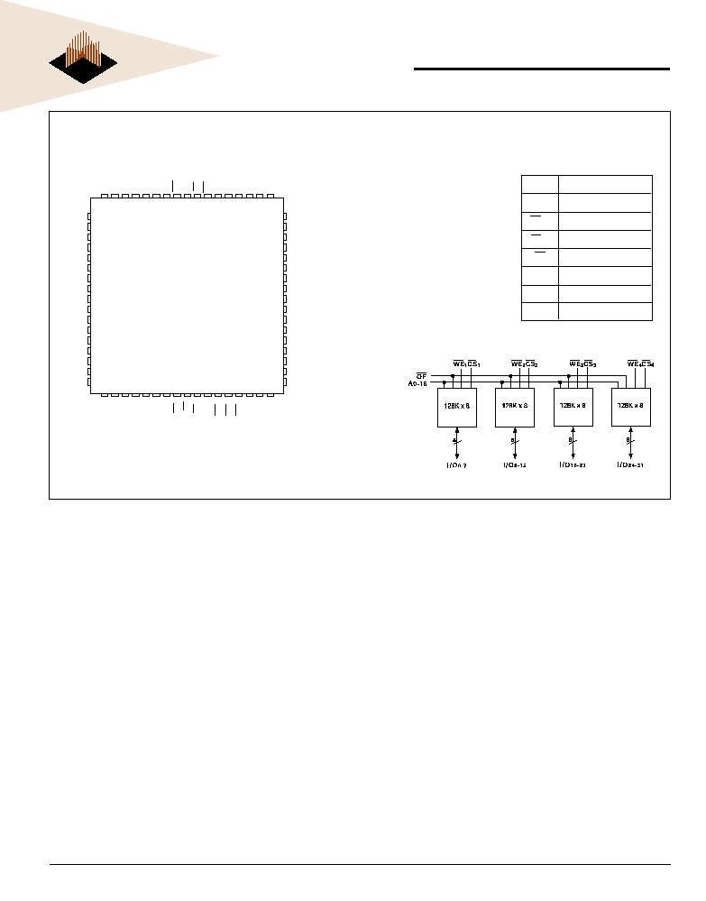
PIN DESCRIPTION
I/O
0-31
Data Inputs/Outputs
A
0-16
Address Inputs
WE
1-4
Write Enables
CS
1-4
Chip Selects
OE
Output Enable
V
CC
Power Supply
GND
Ground
NC
Not Connected
FIG. 3 PIN CONFIGURATION FOR WF128K32-XG1UX5
1
, WF128K32-XG1TX5 AND
WF128K32-XG2UX5, WF128K32-XG2LX5
BLOCK DIAGRAM
TOP VIEW
Note 1: Package Not Recommended For New Design
3
White Electronic Designs Corporation (602) 437-1520 www.whiteedc.com
WF128K32-XXX5
White Electronic Designs
ABSOLUTE MAXIMUM RATINGS (1)
NOTES:
1. Stresses above the absolute maximum rating may cause permanent
damage to the device. Extended operation at the maximum levels may
degrade performance and affect reliability.
2. Minimum DC voltage on input or I/O pins is -0.5V. During voltage
transitions, inputs may overshoot Vss to -2.0 V for periods of up to
20ns. Maximum DC voltage on output and I/O pins is Vcc + 0.5V.
During voltage transitions, outputs may overshoot to Vcc + 2.0 V for
periods of up to 20ns.
3. Minimum DC input voltage on A9 pin is -0.5V. During voltage
transitions, A9 may overshoot Vss to -2V for periods of up to 20ns.
Maximum DC input voltage on A9 is +13.5V which may overshoot to
14.0 V for periods up to 20ns.
DC CHARACTERISTICS - CMOS COMPATIBLE
(V
CC
= 5.0V, V
SS
= 0V, T
A
= -55�C TO +125�C)
NOTES:
1. The ICC current listed includes both the DC operating current and the frequency dependent component (at 5 MHz).
The frequency component typically is less than 2 mA/MHz, with OE at VIH.
2. ICC active while Embedded Algorithm (program or erase) is in progress.
3. DC test conditions: VIL = 0.3V, VIH = VCC - 0.3V
RECOMMENDED OPERATING CONDITIONS
Parameter
Symbol
Min
Max
Unit
Supply Voltage
V
CC
4.5
5.5
V
Input High Voltage
V
IH
2.0
V
CC
+ 0.3
V
Input Low Voltage
V
IL
-0.5
+0.8
V
Operating Temp. (Mil.)
T
A
-55
+125
�C
A
9
Voltage for Sector Protect
V
ID
11.5
12.5
V
Parameter
Unit
Operating Temperature
-55 to +125
�C
Supply Voltage Range (V
CC
)
-2.0 to +7.0
V
Signal voltage range (any pin except A9) (2)
-2.0 to +7.0
V
Storage Temperature Range
-65 to +150
�C
Lead Temperature (soldering, 10 seconds)
+300
�C
Data Retention Mil Temp
10 years
Endurance (write/erase cycles) Mil Temp
10,000 cycles min.
A
9
Voltage for sector protect (V
ID
) (3)
-2.0 to +14.0
V
Parameter
Symbol
Conditions
Unit
Min
Max
Input Leakage Current
I
LI
V
CC
= 5.5, V
IN
= GND to V
CC
10
�A
Output Leakage Current
I
LOx32
V
CC
= 5.5, V
IN
= GND to V
CC
10
�A
V
CC
Active Current for Read
(1)
I
CC1
CS = V
IL
, OE = V
IH
140
mA
V
CC
Active Current for Program
I
CC2
CS = V
IL
, OE = V
IH
200
mA
or Erase
(2)
V
CC
Standby Current
I
CC3
V
CC
= 5.5, CS = V
IH
, f = 5MHz
6.5
mA
V
CC
Static Current
I
CC4
V
CC
= 5.5, CS = V
IH
0.6
mA
Output Low Voltage
V
OL
I
OL
= 8.0 mA, V
CC
= 4.5
0.45
V
Output High Voltage
V
OH1
I
OH
= -2.5 mA, V
CC
= 4.5
0.85 x
V
V
CC
Output High Voltage
V
OH2
I
OH
= -100 �A, V
CC
= 4.5
V
CC
V
-0.4
Low V
CC
Lock Out Voltage
V
LKO
3.2
V
Parameter
Symbol
Conditions
Max Unit
OE capacitance
C
OE
V
IN
= 0 V, f = 1.0 MHz
50
pF
WE
1-4
capacitance
C
WE
V
IN
= 0 V, f = 1.0 MHz
pF
HIP (PGA)
20
CQFP G2U/G1U/G1T/G2L
15
CS
1-4
capacitance
C
CS
V
IN
= 0 V, f = 1.0 MHz
20
pF
Data I/O capacitance
C
I/O
V
I/O
= 0 V, f = 1.0 MHz
20
pF
Address input capacitance
C
AD
V
IN
= 0 V, f = 1.0 MHz
50
pF
This parameter is guaranteed by design but not tested.
CAPACITANCE
(T
A
= +25�C)

4
White Electronic Designs Corporation Phoenix AZ (602) 437-1520
WF128K32-XXX5
White Electronic Designs
AC CHARACTERISTICS WRITE/ERASE/PROGRAM OPERATIONS, CS CONTROLLED
(V
CC
= 5.0V, V
SS
= 0V, T
A
= -55�C TO+125�C)
FIG. 4
Notes:
VZ is programmable from -2V to +7V.
IOL & IOH programmable from 0 to 16mA.
Tester Impedance Z0 = 75 W.
VZ is typically the midpoint of VOH and VOL.
IOL & IOH
are adjusted to simulate a typical resistive load circuit.
ATE tester includes jig capacitance.
AC TEST CONDITIONS
Parameter
Typ
Unit
Input Pulse Levels
V
IL
= 0, V
IH
= 3.0
V
Input Rise and Fall
5
ns
Input and Output Reference Level
1.5
V
Output Timing Reference Level
1.5
V
Parameter
Symbol
-50
-60
-70
-90
-120
-150
Unit
Min
Max
Min
Max
Min Max
Min
Max
Min
Max
Min
Max
Write Cycle Time
t
AVAV
t
WC
50
60
70
90
120
150
ns
WE Setup Time
t
W L E L
t
WS
0
0
0
0
0
0
ns
CS Pulse Width
t
ELEH
t
CP
25
30
35
45
50
50
ns
Address Setup Time
t
AVEL
t
AS
0
0
0
0
0
0
ns
Data Setup Time
t
DVEH
t
DS
25
30
30
45
50
50
ns
Data Hold Time
t
EHDX
t
DH
0
0
0
0
0
0
ns
Address Hold Time
t
E L A X
t
AH
40
45
45
45
50
50
ns
WE Hold from WE High
t
EHWH
t
WH
0
0
0
0
0
0
ns
CS Pulse Width High
t
EHEL
t
CPH
20
20
20
20
20
20
ns
Duration of Programming Operation
t
WHWH1
14
14
14
14
14
14
�s
Duration of Erase Operation
t
WHWH2
2.2
60
2.2
60
2.2
60
2.2
60
2.2
60
2.2
60
sec
Read Recovery before Write
t
GHEL
0
0
0
0
0
0
ns
Chip Programming Time
12.5
12.5
12.5
12.5
12.5
12.5
sec
AC T
EST
C
IRCUIT

5
White Electronic Designs Corporation (602) 437-1520 www.whiteedc.com
WF128K32-XXX5
White Electronic Designs
AC CHARACTERISTICS WRITE/ERASE/PROGRAM OPERATIONS, WE CONTROLLED
(V
CC
= 5.0V, V
SS
= 0V, T
A
= -55�C TO +125�C)
Parameter
Symbol
-50
-60
-70
-90
-120
-150
Unit
Min
Max
Min
Max
Min
Max
Min
Max
Min
Max
Min
Max
Write Cycle Time
t
A V A V
t
WC
50
60
70
90
120
150
ns
Chip Select Setup Time
t
E L W L
t
CS
0
0
0
0
0
0
ns
Write Enable Pulse Width
t
W L W H
t
WP
25
30
35
45
50
50
ns
Address Setup Time
t
A V W L
t
AS
0
0
0
0
0
0
ns
Data Setup Time
t
DVWH
t
DS
25
30
30
45
50
50
ns
Data Hold Time
t
WHDX
t
DH
0
0
0
0
0
0
ns
Address Hold Time
t
W L A X
t
AH
40
45
45
45
50
50
ns
Chip Select Hold Time
t
WHEH
t
CH
0
0
0
0
0
0
ns
Write Enable Pulse Width High
t
W H W L
t
WPH
20
20
20
20
20
20
ns
Duration of Byte Programming Operation (min)
t
WHWH1
14
14
14
14
14
14
�s
Sector Erase Time
t
W H W H 2
2.2
60
2.2
60
2.2
60
2.2
60
2.2
60
2.2
60
sec
Read Recovery Time Before Write
t
G H W L
0
0
0
0
0
0
ns
V
CC
Setup Time
t
VCS
5 0
5 0
5 0
5 0
5 0
5 0
�s
Chip Programming Time
12.5
12.5
12.5
12.5
12.5
12.5
sec
Output Enable Setup Time
t
OES
0
0
0
0
0
0
ns
Output Enable Hold Time (1)
t
OEH
10
10
10
10
10
10
ns
1. For Toggle and Data Polling.
AC CHARACTERISTICS READ ONLY OPERATIONS
(V
CC
= 5.0V, V
SS
= 0V, T
A
= -55�C TO +125�C)
Parameter
Symbol
-50
-60
-70
-90
-120
-150
Unit
Min
Max
Min
Max
Min
Max
Min Max
Min
Max
Min
Max
Read Cycle Time
t
AVAV
t
RC
50
60
70
90
120
150
ns
Address Access Time
t
AVQV
t
ACC
50
60
70
90
120
150
ns
Chip Select Access Time
t
ELQV
t
CE
50
60
70
90
120
150
ns
OE to Output Valid
t
GLQV
t
OE
25
30
35
40
50
55
ns
Chip Select to Output High Z (1)
t
EHQZ
t
DF
20
20
20
25
30
35
ns
OE High to Output High Z (1)
t
GHQZ
t
DF
20
20
20
25
30
35
ns
Output Hold from Address, CS or OE Change,
t
AXQX
t
OH
0
0
0
0
0
0
ns
whichever is first
1. Guaranteed by design, not tested.